background image

6

8

Additional TV Features

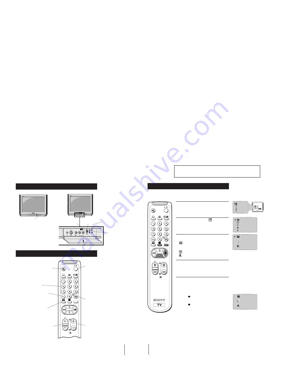
Using Select Mode

You can select different preset picture and sound modes.

1

Press the MENU button on the remote control to
display the menu on the TV screen.

2

With the cursor pointing at the 

SELEC

T

 symbol on the

TV screen as shown, press the yellow button.

3

Press the blue button to select the desired mode:

Personal Mode - reverts to settings made in
 “Adjusting the Picture and Sound” sections of
 the manual
Movie Mode - for films

Live Mode - for live broadcast programmes

4

Press the MENU button to remove the menu
display from the TV screen.

Note:

 The mode selected in step 3 is now stored.

RM-883

PROGR

MENU

/

OFF

SELEC

T

Changing Modes Quickly

1

Press the   button on the remote control to display
the three different modes.

2

Press the   button again to select your desired
mode.

OK

OFF

SELEC

T

OFF

SELEC

T

7

RM-883

PROGR

MENU

/

Basic TV Features

Overview of TV Buttons

On/Off Switch.

Programme Up or
Down Buttons.
(selects TV channels).

Volume Control Buttons.

Auto Tune
Button

Video Input Button.
(selects input signals
from VCR etc.).

Overview of Remote Control Buttons

To Mute Sound

Press to mute TV sound. Press again
to restore the sound.

To Select Channels

Press to select channels.

For double-digit programme
numbers, e.g. 23,  press  -/-- first,
then the buttons 2 and 3.

To Change Screen Format

Press to view programmes in 16:9
mode.
Press again to return to 4:3 mode.

To Adjust TV Volume

Press to adjust the volume of the TV.

To Temporarily Switch Off TV

Press to temporarily switch off TV.  Press
again to switch on TV from standby
mode.
To save energy we recommend switching off
completely when TV is not in use.
NOTE: After 15 -30 minutes without a
TV signal and without any button being
pressed, the TV switches automatically
into standby mode.

To Reveal On Screen Information

Press to reveal all on-screen indications.
Press again to cancel.

To Select Channels

Press to select channels.

g

L/G/S/I R/D/D/D

MONO

+

+

P

_

_

s

2

2

L/G/S/I R/D/D/D

MONO

+

+

P

_

_

s

2

2

g

SECTION 1 GENERAL

The operating instructions mentioned here are partial abstracts
from the Operating Manual. The page numbers of the Operating
Instruction Manual remain as in the manual.

Summary of Contents for Trinitron KV-25K5A

Page 1: ...83 Italian SCC Q06C A KV 25K5B RM 883 French SCC Q02C A KV 25K5D RM 883 AEP SCC Q04C A KV 25K5E RM 883 Spanish SCC Q05C A KV 25K5U RM 883 UK SCC Q01C A KV 29K5A RM 883 Italian SCC Q06B A KV 29K5B RM 883 French SCC Q02B A KV 29K5D RM 883 AEP SCC Q04B A KV 29K5E RM 883 Spanish SCC Q05B A KV 29K5U RM 883 UK SCC Q01B A M I C R O F I L M TRINITRON COLORTV ...

Page 2: ... 89 W 97 W 97 W 97 W 139 W 100 1 W 108 W 108 W 108 W 158 5 W PICTURE TUBE KV 25K5 Super Trinitron Approx 63cm 25 inches Approx 59cm picture measured diagonally 110 degree deflection KV 29K5 Super Trinitron Approx 72cm 29 inches Approx 68cm picture measured diagonally 110 degree deflection Input Output Terminals REAR 21 pin Euro connector CENELEC standard Inputs for Audio and Video signals Inputs f...

Page 3: ...ld be protected by a 5 AMP FUSE at the distribution board ASA T How to replace the fuse Open the fuse compartment with a screwdriver blade and replace the fuse FUSE Model Name Item KV 25K5A KV 29K5A KV 25K5B KV 29K5B KV 25K5D KV 29K5D KV 25K5E KV 29K5E KV 25K5U KV 29K5U Pal Comb OFF OFF OFF OFF OFF PIP OFF OFF OFF OFF OFF RGB Priority OFF OFF OFF ON OFF Woofer Box OFF OFF OFF OFF OFF Scart 1 ON ON...

Page 4: ...input A left Standard level 0 5V rms Output impedence More than 10kohm 7 Blue input 0 7 3dB 75 ohms positive 8 Function select AV control High state 9 5 12V Part mode Low state 0 2V TV mode Input impedence More than 10K ohms Input capacitance Less than 2nF 9 Ground green 10 Open 11 Green Green signal 0 7 3dB 75 ohms positive 12 Open 13 Ground red 14 Ground blanking 15 _ _ Red input 0 7 3dB 75 ohms...

Page 5: ...A SÈCURITÈ LES COMPOSANTS IDENTIFIÈS PAR UNE TRAME ET PAR UNE MARQUE SUR LES SCHÈMAS DE PRINCIPE LES VUES EXPLOSÈES ET LES LISTES DE PIECES SONT D UNE IMPORTANCE CRITIQUE POUR LA SÈCURITÈ DU FONCTIONNEMENT NE LES REMPLACER QUE PAR DES COMPSANTS SONY DONT LE NUMÈRO DE PIÈCE EST INDIQUÈ DANS LE PRÈSENT MANUEL OU DANS DES SUPPLÈMENTS PUBLIÈS PAR SONY Section Title Page Section Title Page 1 GENERAL Ov...

Page 6: ...s Auto Tune Button Video Input Button selects input signals from VCR etc Overview of Remote Control Buttons To Mute Sound Press to mute TV sound Press again to restore the sound To Select Channels Press to select channels For double digit programme numbers e g 23 press first then the buttons 2 and 3 To Change Screen Format Press to view programmes in 16 9 mode Press again to return to 4 3 mode To ...

Page 7: ...IIIIIIIIIIIII IIIIIIIIIIIIIII IIIIIIIIIIIIIII IIIIIIIIIIIIIII IIIIIIIIIIIIIII 0 10 Adjusting the Sound Although the sound is adjusted at the factory you can modify it to suit your own requirement Additional TV Features Symbol Item Mono sound Stereo sound A Channel 1 sound B Channel 2 sound to select your desired language from a dual sound broadcast DSP On Off digital sound processor Treble Bass Ba...

Page 8: ... Press the button on the remote control to switch on teletext 3 Input three digits for the page number using the numbered buttons on the control 4 Press the button to switch off teletext Note Teletext errors may occur if the broadcasting signals are weak Using Other Teletext Functions To Superimpose Teletext on to the TV Press once in teletext mode or twice in TV mode to superimpose teletext on to...

Page 9: ...the yellow button 3 With the cursor pointing at PROGR on the TV screen as shown press PROGR or button on the remote control to allocate a programme number to the channel eg PROGR 01 For double digit numbers e g 55 press the button on the remote control then the corresponding numbered buttons 4 Press the blue button to select the channel type C to preset a regular channel or S to preset a cable cha...

Page 10: ...correct input symbol appears on the TV screen Symbol Input signals 1 Audio video input signal through the Euro AV connector F RGB input signal through the Euro AV connector F 2 Audio video input signal through the Euro AV connector E or the phono sockets C and D s S video input signal through the socket B 3 Switch on the connected equipment 4 To return to normal TV picture press the button on the ...

Page 11: ... changing Turn off any equipment connected to the 21 pin programmes or selecting teletext Euro connector on the rear of the TV Remote control does not function Replace the batteries If you continue to have these problems have your TV serviced by qualified personnel NEVER open the casing yourself 19 Specifications TV system I Colour system PAL NTSC 3 58 4 43 only Video In Channel coverage UHF B21 B...

Page 12: ...12 KV 25K5 29K5 SECTION 2 DISASSEMBLY 3 Rear Cover 1 1 Screw BTV 4x16 2 1 REAR COVER REMOVAL 2 2 CHASSIS ASSY REMOVAL 2 8 Screws BTV 4x16 ...

Page 13: ...13 KV 25K5 29K5 2 4 H1 BOARD REMOVAL 2 5 S1 BOARD REMOVAL 2 3 SERVICE POSITION To release push the claws in the direction of the arrow as indicated Release the clip indicated ...

Page 14: ...arbon paint on the CRT after removing the anode REMOVAL OF ANODE CAP HOW TO HANDLE THE ANODE CAP 1 To prevent damaging the surface of the anode cap do not use sharp materials 2 Do not apply too great a pressure on the rubber as this may cause damage to the anode connector 3 A metal fitting called a shatter hook terminal is fitted inside the rubber cap Do not turn the rubber foot over excessively t...

Page 15: ...the gates with a sharp wire cutter at the locations shown and indicated by arrows Note There are 2 plates fitted to the main bracket and secured by 4 gates Only remove the necessary plate to gain access to the printed wiring board 2 REFITTING THE PLATES Because the plates differ in size it is important that the correct plates are refitted in their original location Please note that the plates need...

Page 16: ...flection Yoke G1 Neck Assy A buckle G2 For 29 models align the neck assy as indicated below Preparation 1 In order to reduce the influence of geomagnetism on the set s picture tube face it in an easterly or westerly direction 2 Switch on the TV set s power and degauss with the degausser 3 1 BEAM LANDING 1 Input an all white signal from the pattern generator Set the Contrast and Brightness to norma...

Page 17: ...ertically adjust the V STAT magnet so that the Red Green and Blue points are on top of each other at the centre of the screen 3 If the H STAT variable resistor is unable to bring the Red Green and Blue points together at the centre of the screen adjust the horizontal convergence with the H STAT variable resistor and the V STAT magnet in the manner indicated below In this case the H STAT variable r...

Page 18: ... STAT VR to adjust the Red Green and Blue dots so that they coincide at the centre of the screen by moving the dots in the horizontal direction 3 Dynamic convergence adjustment Preparation Before starting this adjustment adjust the horizontal and vertical static convergence 1 Slightly loosen the deflection yolk screws 2 Remove the deflection yolk spacer 3 Move the deflection yolk as indicated in t...

Page 19: ...de 3 Enter into the Picture service menu 4 Select the Green drive and adjust so that the White Balance becomes optimum 5 Select the Blue drive and adjust so that the White Balance becomes optimum 6 Set the Picture to MIN 7 Set the R cut off to 07 8 Adjust the G cut off and the B cut off so that the White Balance becomes optimum 10 Press the button to return to TV operation 3 4 FOCUS 1 Input a Phil...

Page 20: ...s the Yellow button to enter into the required menu item 6 Press the Menu button on the Remote Commander to quit the Service Mode when all adjustments have been completed Note The data shown in the TV STATUS table is dependant on destination and country TEST MENU Picture Geometry Sound TV Status AGC Adjust Technical PICTURE R Drive Adj G Drive Adj B Drive Adj R cut off Adj G cut off Adj B cut off ...

Page 21: ...e colour bars are of equal levels as indicated below Note Ensure that no signal is applied to the Antenna socket while carrying out the following IF adjustments SYSTEM B G D K I L I F ADJUSTMENT 1 Input a 38 9Mhz carrier signal at 100dBuV to Pin 11 IF output of the tuner TU101 2 Measure the voltage at Pin 17 of IC101 3 Adjust L103 A Board to obtain a voltage of 2 5V 0 3V SYSTEM L BAND 1 I F ADJUST...

Page 22: ...JUSTMENT 1 Enter into the Geometry service menu 2 Select and adjust each item in order to obtain the optimum image GEOMETRY V centre Adj V size Adj V Lin Adj S Corr Adj H Cent Adj H Size Adj Pin Amp Adj Corner Pin Adj Pin Phase Adj V Bow Adj V Angle Adj Upper V Lin Adj Lower V Lin Adj Left HBLK 07 Right HBLK 07 CD Mode AV 01 ...

Page 23: ...est 37 No function 38 No function 39 No function 40 No function 41 Re initialize the NVM Only when Prog 59 42 Re initialise geometry settings Only when Prog 59 43 No function 44 No function 45 No function 46 No function 47 No function 48 Set NVM as NON Virgin Only when Prog 59 49 Set NVM as Virgin Only when Prog 59 50 No function 51 No function 52 No function 53 No function 54 No function 55 No fu...

Page 24: ...s acknowledge at Power ON 07 Jungle controller no IIC acknowledge at Power ON 08 Tuner no acknowledge at Power ON 09 Sound processor no acknowledge at Power ON 10 Error Times 2 3 4 5 6 7 8 9 10 4 3 FE 1 SELF DIAGNOSTIC SOFTWARE The identification of errors within the FE 1 chassis is triggered in one of two ways 1 Busy or 2 Device failure to respond to IIC In the event of one of these situations ar...

Page 25: ...DY ASSY V DY H DY H DY H DY V DY V DY H DY H DY TO C BOARD CN701 1000V 200V H1 TO PICTURE TUBE TO VM BOARD CN1809 TO VM BOARD CN1803 2 3 6 5 1 7 IC531 PIN CORRECTION EW HP PROTECT IN VP VD 3 2 1 4 T531 HDT IC609 STANDBY POWER HD D C T602 D632 RECT DGC DGC DGC CHECK DGC CHECK TO H1 BOARD CN604 IC001 MICRO CONTROLLER SCLO SDAO SDA SCL MON OUT SCL SDA CN201 CN208 CN606 CN603 CN602 J404 J401 CN101 CN5...

Page 26: ...IZED POLYESTER MPP METALIZED POLYPROPYLENE ALB BIPOLAR ALT HIGH TEMPERATURE ALR HIGH RIPPLE 6 5 3 2 7 1 9V 9V VM AMP Q1701 1702 1708 1709 VM AMP BUFFER Q1704 BUFFER Q1840 1841 6 5 2 7 1 IC1902 DF COMPARATOR 3 9V 15V PULSE 7 6 5 1 V PULSE NS CORRECT VM 2 4 6 8 T1901 1 DF CN1809 TO A BOARD CN503 TO A BOARD CN505 3 1 CN1801 QP QP VM NECK ASSY QP QP GND VM TO ROTATION COIL CN1803 IC1901 COMPARATOR ROT...

Page 27: ......

Page 28: ......

Page 29: ......

Page 30: ......

Page 31: ......

Page 32: ... 0 Vp p H 142 Vp p H 11 1 1KVp p H SECAM 2 6 Vp p H 2 0 Vp p H 4 7 3 56 Vp p V 290 Vp p H 1 1 3 Vp p H SECAM PAL PAL 2 2 1 3 Vp p H 6 8 10 12 Vp p H 12 13 14 2 4 Vp p H 15 3 0 Vp p H SECAM PAL 15 9 5 1 4 Vp p H 3 93 Vp p H 24 Vp p H 4 102 Vp p H 1 95 Vp p H 2 WAVEFORMS C BOARD ...

Page 33: ...TZJ T 77 7 5C MTZJ T 77 9 1A MTZJ T 77 9 1A MTZJ T 77 10 DAN202K DAN202K T146 AK04 V1 AU 012 V1 BYD33G BYD33G AMMO DINL20 TR ERB44 06TP1 EG 1Z V1 EL1Z ERD28 06S LM358DR EZ NJM4558M TE2 NJM2903D TOP VIEW 1 4 8 5 SAA5497PS MIA 038 SAA5497PS MIA 039 SAA5497PS MIA040 TOP VIEW 52 27 1 26 STR F6654 TDA7495 TDA9818 V1 TDA9817 V1 TOP VIEW 1 12 24 13 TOP209P TOP VIEW 1 4 8 5 TYA7805CTV TYA7809CTV B C E 2SK...

Page 34: ...S I T EW PARABOLA FUNC H SIZE TRAPEZIUM PIN AMP EW DC CORNER PIN 48 47 46 5 1 15 39 38 37 28 27 26 25 32 31 30 29 23 24 35 14 11 19 18 20 36 42 3 CLAMP RGB 2 2 ABL PEAK LIM ABL MODE ABL VTH 17 5 IREF REG 33 10 12 16 13 4 7 9 6 41 2 43 HD GEN HD W V SAW GEN 50 50 VTIM H TIM GEN H BLK LEFT HBLK RIGHT HBLK AFC APC GAIN FH HIGH H CENT 21 22 34 VD SAW FUNC VON S CORRECTION VSIZE V LINEARITY V POSITION ...

Page 35: ...5E 25K5U 1 453 265 11 TRANSFORMER ASSY FLYBACK NX 1681 U2B4 KV 29K5A 29K5B 29K5D 29K5E 29K5U 6 1 693 418 11 TUNER TELE9 001A KV 25K5A 25K5B 25K5D 25K5E 29K5A 29K5B 29K5D 29K5E 8 598 464 00 TUNER FSS BTP AU611 KV 25K5U 29K5U 7 A 1652 055 A S1 BOARD COMPLETE KV 25K5A 25K5D 29K5A 29K5D A 1652 059 A S1 BOARD COMPLETE KV 25K5B 29K5B A 1652 054 A S1 BOARD COMPLETE KV 25K5E 25K5U 29K5E 29K5U 8 A 1632 740...

Page 36: ...25GXABA KV 25K5A 25K5B 25K5D 25K5E 25K5U 8 451 466 11 DEFLECTION YOKE Y29GXC2B KV 29K5A 29K5B 29K5D 29K5E 29K5U 60 8 733 254 76 ITC KV 25K5A 25K5B 25K5D 25K5E 25K5U 8 733 856 75 ITC KV 29K5A 29K5B 29K5D 29K5E 29K5U 61 8 453 005 21 NECK ASSY PICTURE TUBE NA297 M2 KV 29K5A 29K5B 29K5D 29K5E 29K5U 62 A 1644 090 A VM BOARD COMPLETE KV 29K5A 29K5B 29K5D 29K5E 29K5U 63 A 1638 112 A C BOARD COMPLETE 64 4...

Page 37: ...016 1 164 004 11 CERAMIC CHIP 0 1MF 10 25V C018 1 164 232 11 CERAMIC CHIP 0 01MF 10 50V C019 1 163 038 00 CERAMIC CHIP 0 1MF 25V C022 1 126 935 11 ELECT 470MF 20 16V C024 1 104 665 11 ELECT 100MF 20 25V C025 1 126 960 11 ELECT 1MF 20 50V C028 1 163 117 00 CERAMIC CHIP 100PF 5 50V KV 29K5A 29K5B 29K5D 29K5E 29K5U C029 1 163 077 00 CERAMIC CHIP 0 1MF 10 25V C030 1 104 665 11 ELECT 100MF 20 25V C031 ...

Page 38: ...91 CERAMIC CHIP 0 0047MF 10 50V C335 1 164 232 11 CERAMIC CHIP 0 01MF 10 50V C336 1 164 232 11 CERAMIC CHIP 0 01MF 10 50V C337 1 164 232 11 CERAMIC CHIP 0 01MF 10 50V C338 1 126 967 11 ELECT 47MF 20 50V C339 1 163 038 00 CERAMIC CHIP 0 1MF 25V C350 1 163 017 91 CERAMIC CHIP 0 0047MF 10 50V C351 1 163 017 91 CERAMIC CHIP 0 0047MF 10 50V C401 1 163 141 00 CERAMIC CHIP 0 001MF 5 50V C402 1 126 960 11...

Page 39: ...K5D 25K5E 25K5U C580 1 164 232 11 CERAMIC CHIP 0 01MF 10 50V C582 1 163 275 11 CERAMIC CHIP 0 001MF 5 50V C584 1 126 963 11 ELECT 4 7MF 20 50V C601 1 107 563 11 FILM 0 1MF 20 300V C602 1 107 563 11 FILM 0 1MF 20 300V C603 1 117 700 51 CERAMIC 0 0022MF 99 250V C604 1 117 700 51 CERAMIC 0 0022MF 99 250V C605 1 104 652 11 ELECT 470MF 20 10V C606 1 125 555 11 ELECT BLOCK 330MF 20 400V C607 1 125 787 5...

Page 40: ...1SS133T 77 D320 8 719 929 15 DIODE HZS9 INB2 D405 8 719 109 97 DIODE RD6 8ES B2 D406 8 719 109 97 DIODE RD6 8ES B2 D407 8 719 109 97 DIODE RD6 8ES B2 D409 8 719 109 97 DIODE RD6 8ES B2 D414 8 719 109 97 DIODE RD6 8ES B2 D415 8 719 929 15 DIODE HZS9 INBZ D417 8 719 929 15 DIODE HZS9 INB2 D422 8 719 109 97 DIODE RD6 8ES B2 D423 8 719 109 97 DIODE RD6 8ES B2 D427 8 719 109 97 DIODE RD6 8ES B2 D501 8 ...

Page 41: ...12 521 31 INDUCTOR 4 7UH L532 1 412 552 11 INDUCTOR 2 2MMH KV 25K5A 25K5B 25K5D 25K5E 25K5U 1 412 553 11 INDUCTOR 3 3MMH KV 29K5A 29K5B 29K5D 29K5E 29K5U L533 1 406 989 21 INDUCTOR 0UH L535 1 459 111 00 INDUCTOR 0UH L537 1 409 756 11 COIL HORIZONTAL LINEARITY KV 25K5A 25K5D 25K5E 25K5U 1 416 214 11 COIL HORIZONTAL LINEARITY KV 25K5B 1 409 855 11 COIL HORIZONTAL LINEARITY KV 29K5A 29K5B 29K5D 29K5E...

Page 42: ... CHIP 470 5 1 10W R051 1 216 049 00 RES CHIP 1K 5 1 10W R053 1 216 065 00 RES CHIP 4 7K 5 1 10W R054 1 216 041 00 RES CHIP 470 5 1 10W R055 1 216 081 00 RES CHIP 22K 5 1 10W R056 1 216 105 00 RES CHIP 220K 5 1 10W R057 1 216 075 00 RES CHIP 12K 5 1 10W R058 1 216 063 91 RES CHIP 3 9K 5 1 10W R059 1 216 089 00 RES CHIP 47K 5 1 10W R060 1 216 174 00 RES CHIP 100 5 1 8W R061 1 216 174 00 RES CHIP 100...

Page 43: ... 216 085 00 RES CHIP 33K 5 1 10W R207 1 216 295 00 SHORT 0 R209 1 216 065 00 RES CHIP 4 7K 5 1 10W R211 1 215 873 00 METAL OXIDE 4 7K 5 1W F R213 1 216 089 00 RES CHIP 47K 5 1 10W R301 1 216 025 00 RES CHIP 100 5 1 10W R302 1 216 081 00 RES CHIP 22K 5 1 10W R303 1 216 073 00 RES CHIP 10K 5 1 10W R304 1 216 073 00 RES CHIP 10K 5 1 10W R306 1 216 206 00 RES CHIP 2 2K 5 1 8W R309 1 216 675 11 METAL C...

Page 44: ...1 1 215 869 11 METAL OXIDE 1K 5 1W F R512 1 249 377 11 CARBON 0 47 5 1 4W F R513 1 216 097 00 RES CHIP 100K 5 1 10W R514 1 249 377 11 CARBON 0 47 5 1 4W F R515 1 249 377 11 CARBON 0 47 5 1 4W F R516 1 249 493 11 CARBON 56K 5 1 2W R517 1 249 434 11 CARBON 27K 5 1 4W KV 25K5A 25K5B 25K5D 25K5E 25K5U 1 249 429 11 CARBON 10K 5 1 4W KV 29K5A 29K5B 29K5D 29K5E 29K5U R518 1 216 065 00 RES CHIP 4 7K 5 1 1...

Page 45: ...5 11 CARBON 680 5 1 4W R613 1 240 030 91 METAL 4 7M 5 1 2W R614 1 240 030 91 METAL 4 7M 5 1 2W R615 1 249 422 11 CARBON 2 7K 5 1 4W R616 1 216 393 00 METAL OXIDE 2 2 5 3W F R617 1 249 405 11 CARBON 100 5 1 4W F R619 1 216 065 00 RES CHIP 4 7K 5 1 10W R622 1 249 401 11 CARBON 47 5 1 4W R627 1 249 389 11 CARBON 4 7 5 1 4W F R628 1 247 791 91 CARBON 22 5 1 4W R652 1 216 393 00 METAL OXIDE 2 2 5 3W F ...

Page 46: ...06 70 TRANSISTOR BF871 127 Q704 8 729 200 17 TRANSISTOR BF421L AMMO Q705 8 729 119 78 TRANSISTOR 2SC2785 HFE Q706 8 729 906 70 TRANSISTOR BF871 127 Q707 8 729 200 17 TRANSISTOR BF421L AMMO Q708 8 729 119 78 TRANSISTOR 2SC2785 HFE Q709 8 729 906 70 TRANSISTOR BF871 127 Q710 8 729 200 17 TRANSISTOR BF421L AMMO RESISTOR R701 1 247 895 91 CARBON 470K 5 1 4W R704 1 216 486 00 METAL OXIDE 8 2K 5 3W F R7...

Page 47: ...00 FILM 0 001MF 5 630V C1913 1 129 703 00 FILM 0 0012MF 5 630V C1914 1 102 157 00 CERAMIC 560PF 10 500V C1915 1 137 102 11 FILM 0 022MF 10 250V C1951 1 126 964 11 ELECT 10MF 20 50V C1952 1 164 232 11 CERAMIC CHIP 0 01MF 10 50V C1953 1 136 165 00 FILM 0 1MF 5 50V C1954 1 164 232 11 CERAMIC CHIP 0 01MF 10 50V C1955 1 136 165 00 FILM 0 1MF 5 50V C1956 1 126 964 11 ELECT 10MF 20 50V C1957 1 126 964 11...

Page 48: ... 1 10W R1731 1 249 411 11 CARBON 330 5 1 4W R1751 1 216 049 71 RES CHIP 1K 5 1 10W R1752 1 216 049 71 RES CHIP 1K 5 1 10W R1753 1 216 049 71 RES CHIP 1K 5 1 10W R1805 1 216 073 00 RES CHIP 10K 5 1 10W R1806 1 216 105 91 RES CHIP 220K 5 1 10W R1807 1 216 073 00 RES CHIP 10K 5 1 10W R1808 1 216 073 00 RES CHIP 10K 5 1 10W R1809 1 216 073 00 RES CHIP 10K 5 1 10W R1810 1 216 073 00 RES CHIP 10K 5 1 10...

Page 49: ...DE SEL1210S D 4 203 258 01 HOLDER LED D901 D902 8 719 929 15 DIODE HZS9 INBZ D903 8 719 929 15 DIODE HZS9 INBZ D904 8 719 109 97 DIODE RD6 8ES B2 D905 8 719 109 97 DIODE RD6 8ES B2 D906 8 719 923 60 DIODE MTZJ T 77 9 1A D907 8 719 923 60 DIODE MTZJ T 77 9 1A D908 8 719 923 60 DIODE MTZJ T 77 9 1A FUSE F601 1 576 231 21 FUSE H B C 4AMP 250V 1 535 725 11 FUSE HOLDER F601 IC IC900 8 742 014 11 HYB IC...

Page 50: ...43 1 163 005 11 CERAMIC CHIP 470PF 10 50V C1144 1 163 005 11 CERAMIC CHIP 470PF 10 50V C1145 1 163 077 00 CERAMIC CHIP 0 1MF 10 25V C1146 1 164 005 11 CERAMIC CHIP 0 47MF 25V C1147 1 164 005 11 CERAMIC CHIP 0 47MF 25V C1148 1 164 005 11 CERAMIC CHIP 0 47MF 25V C1149 1 126 960 11 ELECT 1MF 20 50V C1150 1 126 960 11 ELECT 1MF 20 50V C1151 1 104 664 11 ELECT 47MF 20 25V C1152 1 164 004 11 CERAMIC CHI...

Page 51: ... CHIP 10K 5 1 10W R1125 1 216 065 71 RES CHIP 4 7K 5 1 10W R1126 1 216 073 71 RES CHIP 10K 5 1 10W R1130 1 216 073 71 RES CHIP 10K 5 1 10W KV 25K5A 25K5D 29K5A 29K5D R1134 1 216 073 71 RES CHIP 10K 5 1 10W KV 25K5A 25K5D 29K5A 29K5D R1152 1 216 035 00 RES CHIP 270 5 1 10W KV 25K5B 29K5B R1153 1 216 025 00 RES CHIP 100 5 1 10W KV 25K5B 29K5B R1154 1 216 067 00 RES CHIP 5 6K 5 1 10W KV 25K5B 29K5B R...

Page 52: ...PICTURE TUBE SD 269 M68LCT60X KV 29K5A 29K5B 29K5D 29K5E 29K5U 8 451 404 23 DEFLECTION YOKE Y25GXABA KV 25K5A 25K5B 25K5D 25K5E 25K5U 8 451 466 11 DEFLECTION YOKE Y29GXC2B KV 29K5A 29K5B 29K5D 29K5E 29K5U 8 733 254 76 ITC KV 25K5A 25K5B 25K5D 25K5E 25K5U 8 733 856 75 ITC KV 29K5A 29K5B 29K5D 29K5E 29K5U ACCESSORIES AND PACKAGING MATERIALS 4 395 957 01 BAG PROTECTION KV 25K5A 25K5B 25K5D 25K5E 25K5...

Page 53: ...74 KV 25K5 29K5 Sony Corporation Sony UK Service Promotions Dept 9 974 963 01 English 98BP7169 1 Printed in U K 1998 2 ...

Reviews: