5-1
5-2
5-3
5-4
SECTION 5
DIAGRAMS
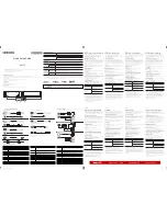
5-1. BLOCK DIAGRAMS
5-2. CIRCUIT BOARDS LOCATION
5-3. SCHEMATIC DIAGRAMS AND
PRINTED WIRING BOARDS
Note:
• All capacitors are in µF unless otherwise noted. (pF: µµF)
Capacitors without voltage indication are all 50 V.
• Indication of resistance, which does not have one for rating
electrical power, is as follows.
Pitch: 5 mm
Rating electrical power 1/4 W (CHIP : 1/10 W)
• All resistors are in ohms.
•
f
: nonflammable resistor.
•
5
: fusible resistor.
•
¢
: internal component.
•
p
: panel designation, and adjustment for repair.
• All variable and adjustable resistors have characteristic curve B,
unless otherwise noted.
•
e
: earth-ground.
•
E
: earth-chassis.
• The components identified by
[
in this basic schematic diagram
have been carefully factory-selected for each set in order to
satisfy regulations regarding X-ray radiation.
Should replacement be required, replace only with the value
originally used.
• When replacing components identified by
]
, make the
necessary adjustments indicated. (See page 3-1)
• When replacing the part in below table, be sure to perform the
related adjustment.
Note: The components identified by shading and mark
¡
are critical for safety. Replace only with part
number specified.
D
A
J
• All voltages are in V.
• Readings are taken with a 10 M digital multimeter.
• Readings are taken with a color-bar signal input.
• Voltage variations may be noted due to normal production
tolerances.
•
*
: Can not be measured.
• Circled numbers are waveform references.
•
s
: B + bus.
•
S
: B – bus.
G
D
S
2
3
4
5
6
7
8
9
0
!¡
!™
!¢
!§
–
1
G
D
S
G
S
S
D
G
D
Ver.1.5
Transistor
(FET)
Transistor
Transistor
Discrete semiconductot
(Chip semiconductors that are not actually used are included.)
Diode
Diode
Diode
Diode
Diode
Diode
Diode
Diode
Diode
Diode
Source
Source
Anode
Anode
(NC)
(NC)
Cathode
Anode
Cathode
Common
Cathode
Cathode
Common
Cathode
Cathode
Common
Common
Common
Common
Cathode
Anode
Base
Emitter
Collector
Base
Emitter
Collector
Drain
Gate
Gate
Drain
Device
Printed symbol
Terminal name
Circuit
Terminal name of semiconductors in silk screen
printed circuit ( )
Anode
Anode
Anode
Cathode
Anode
Anode
Cathode
!£
Transistor
(FET)
Transistor
(FET)
!∞
Emitter
Collector
Base
Transistor
Source
Gate
Drain
Cathode
Anode
Anode
Cathode
Anode
Anode
*
D BOARD
Part Replaced (
[
)
RV501 (HV ADJ)
Part Replaced (
]
)
IC501, IC605, IC901, D517, C535, C540, C541,
C542, C544, C553, C554, C555, C558, C561, R545,
R546, R547, R548, R549, R550, R552, R564, R567,
RV501, T501 (FBT)
1
2
3
1
2
3
4
5
6
7
8
9
1
2
3
4
5
6
7
1
2
3
4
5
6
1
2
3
4
1
2
3
4
5
6
7
8
1
1
2
3
4
5
6
7
8
9
10
11
12
13
14
15
DDC SCL
DDC SDA
HOST GND
HD
VD
GND
RED
R GND
GREEN
G GND
BLUE
B GND
SHRP1
BPCLP
GND
GND
GND
SIGNAL IN
HD15
PIG-TAIL
NC
DDC SCL
DDC SDA
HOST GND
C BLK
C SYNC
V SYNC
H SYNC
IIC SCL
IIC SDA
R1_IN
G1_IN
B1_IN
R2_IN
CLAMP
SIGNAL_SW
R_OUT
G_OUT
B_OUT
T_SW & LEVEL
R_IN
G_IN
B_IN
SCL
SDA
BLK
CLAMP
VFLB
SDA
SCL
HFLB
INV.
Q004
IC006
RGB PRE AMP
IC001
OSD MIX
IC003
OSD
OSD_BLK
B_OSD
G_OSD
R_OSD
R_OUT
G_OUT
B_OUT
R_BLK
G_BLK
G2
R_OSD
G_OSD
B_OSD
OSD_BLK
R_OUT
G_OUT
B_OUT
R_OUT
G_OUT
B_OUT
R_IN
G_IN
B_IN
RIN
G_IN
B_IN
IC002
RGB-OUT
IC004
RGB CUT OFF CONT
J001
IC005
G2 CUT OFF
Q001
SOFT KILLER
+180V
NC
+80V
GND
H1
+12V
GND
1.2KV
STBY+5V
CN301
WHT :S-MICRO
CN305 8P
+180V
+80V
+12V
STBY+5V
A
(VIDEO)
1
2
3
1
2
4
IC603
1
2
5
D912
LED DRV
(RED)
Q902
LED DRV
(GREEN)
Q901
FUNCTION
SW
IC601
OUTPUT
DEMAGIN
E/A OUT
FOLD BACK IN
D610
D611
SWITCHING
CONVERTER
D651
AC RECT
S601
TH600
LF602
LFT
F601
L
G
N
TH601
RY601
RELAY
DRIVE
Q601
CN601
3P
DGC2
NC
DGC1
CN600
AC IN
DGC
CN602
2P
THP600A
THP600
T601
SRT
D612
D613
D614
D615
D616
D617
D618
D654
Q604
3
1
2
3
7
5
6
8
13
7
15
48
47
9
8
7
5
4
3
2
10
11
12
13
14
15
16
17
18
1
2
5
7
12
13
14
21
19
17
6
8
10
2
1
16
11
10
7
8
5
25
22
18
3
4
5
28
12
13
14
15
12
13
14
15
1
2
3
8
9
5
3
1
7
8
9
4
10
KR
KG
KB
G2
9
8
7
6
5
7
+180V
+80V
+15V
HEATER
-15V
IN
OUT
IC802
+5V REG
IC605
1,2
3
6
7
5
1
3
4
2
VDD
+IN
VSS
OUT
-IN
DISABLE
INPUT1,2
OUTPUT1
OUTPUT2
+5V
+5V-2
L902
L510
H CENT
Q506
H CENT
Q518
H CENT SW
Q517
Q519
BUFFER
Q505
DF AMP
Q504
RELAY DRIVE
IC503
H CENT AMP
1
2
3
4
5
6
7
1
2
3
4
1
2
3
4
5
6
7
8
9
10
IC901
CPU
46
5
22
28
20
30
45
44
38
39
54
34
35
33
37
36
SDA
SCL
CN903 7P
WHT :S-MICRO
SHRP1
GND
C BLANK
BP CLAMP
C SYNC
V SYNC
H SYNC
CN307 9P WHT :S-MICRO
CN311 3P WHT :S-MICRO
CN310 4P
WHT :S-MICRO
CN309 7P WHT :S-MICRO
CN306 6P WHT :S-MICRO
CN901 4P
WHT
WHT :S-MICRO
CN902 10P
D GND
+5V
RXD
TXD
DDC SCL
DDC SDA
HOST GND
NC
IIC DATA
GND
IIC CLK
GND
IC900
4
1,2
IC905 EEPROM
X901
24MHz
IC904 RESET
1
3
IN
OUT
SDA
SCL
5
6
+5V-2
DEGAUSS
KEY SCAN
LED R
LED G
C BLK
SHRP1
CLP
CSI
VSI1
HSI1
OSC IN
OSC OUT
RDI
TDO
RESET
DDC SCL
DDC SDA
HOST GND
SDA
SCL
6
4
9
17
5
4
7
2
32
27
25
26
2
19
29
3
4
14
26
28
12
27
10
9
2
17
8
IC902
X5
SDA
SCL
H.FLY
H.IN
V.IN
SDA
SCL
V.DF
V.DIV
V.SIN
E/W
LOCK
H.OUT
V.SAW
X902
TH501
INV.
Q903
H DRIVE
Q511
H DRIVE OUT
IC401 V OUT
-IN
+IN
OUT
PUMP UP OUT
REMOTE ON/OFF
H CENT
H CENT SW
THERMAL
HFB
HSO
PD3
VSO
AUDIO
VFB
PA4
PA0-PA3
ITA
HV
ABL
HEATER
4
1
6
8
H OUT
Q507
S CAP
CHANGE
Q512-516
12
11
10
9
8
7
1
5
L508
HLC2
RY500
L509
HLC1
T505 HST
1
2
5
3
BUFFER
Q521
T503 DFT
T504 HDT
H BLK
Q508
16
17
14
3
2
5
SDA
SCL
SDA
SCL
V_SIN
VREF OUT
IC701
CONVERGENCE CONTROL
6
7
8
9
H_STATIC OUT
V_STATIC OUT
H_CONV OUT
V_CONV OUT
2
1
5
6
11
10
14
15
3
4
12
13
IC702
IC801
5
4
6
2
8
16
9
13
1
2
3
4
5
6
7
8
1
2
3
4
5
6
VP
VI(1)
VI(2)
VC1
VC2
OUT1
OUT2
OUT1-
CN701 8P
WHT :S-MICRO
CY1 +
CY1 -
CY2 +
CY2 -
CY3 +
CY3 -
CY4 +
CY4 -
CN802 6P
WHT :S-MICRO
RET
R OUT
L OUT
R IN
-R OUT
L IN
1
2
3
4
5
6
RET
R OUT
L OUT
R IN
-R OUT
L IN
6P
15
14
3
2
8
4
20
19
18
IC501
PWM CONT
REF
24
23
12
D524
L503
H REG OUT
2
5
HV REG
Q503
HV OUT
Q510
L501
L502
D515
T501
FBT
1
2
5
HV
13
16
FV
15
14
11
FOCUS
TO CRT
RV501
HV ADJ
1
CN510 1P
1.2KV
Q522,523
49
50-53
23
18
16
24
3
1
2
3
4
5
6
6P :DY
H DY +
H DY +
H DY -
H DY -
V DY -
V DY +
+12V
HEATER SW
Q605,606
HEATER
1
2
3
4
5
6
7
8
9
+180V
+80V
+12V
+5V-2
CN502 9P
WHT :S-MICRO
+180V
NC
+80V
NC
GND
H1
+12V
GND
+5V
1
2
CN503 2P
ROTATION -
RO
ROTATION
DRIVE
IC502
2
4
D
POWER
DEFLECTION
D517
+5V
1
2
J
(AUDIO)
CN1002
2P
S
SPEAKER -
J1001
J1002
SPEAKER
H DY
V DY
CN1001
:MINI
CN501
HD.IN
VPOSIN
Q520
+12V
Q501,502
ROTATION
HRTRC
VRTRC
OVP
CUR SENSE IN
5V/12V REG
VRTRC
HRTRC
B_BLK
11
AUDIO OUT
CY AMP
REG SW
IC604 SENSOR
H1
HEADPHONE
AUDIO IN
MUTE
SYNC
BUFFER
Q602
SYNC PROCESS
B-SS3431<AUS>-B/D
Summary of Contents for Trinitron CPD-200GS
Page 22: ...5 16 5 4 SEMICONDUCTORS ...
Page 23: ...5 17 ...