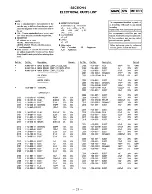


8
8
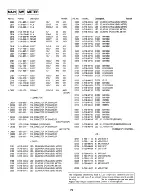
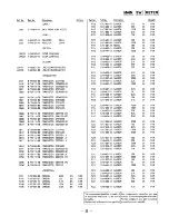
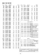
TC-WE305
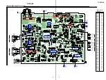
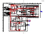
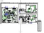
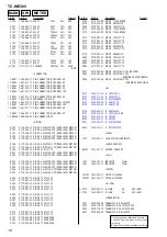
For schematic diagrams.
Note:
• All capacitors are in
µ
F unless otherwise noted. pF:
µµ
F 50 WV or
less are not indicated except for electrolytics and tantalums.
• All resistors are in
Ω
and
1
/
4
W or less unless otherwise specifed.
•
%
: indicates tolerance.
•
f
: internal component.
•
1
: fusible resistor.
•
C
: panel designation.
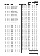
Note:
The components identified by mark
0
or dotted
line with mark
0
are critical for safety.
Replace only with part number specified.
•
A
: B+ Line.
•
B
: B– Line.
•
H
: adjustment for repair.
• Voltages are dc with respect to ground under no-signal conditions.
no mark : PLAY
(
) : REC
• Voltages are taken with a VOM (Input impedance 10 M
Ω
).
Voltage variations may be noted due to normal production
tolerances.
• Waveforms are taken with a oscilloscope.
Voltage variations may be noted due to normal production toler
ances.
•
Circled numbers refer to waveforms.
•
Signal path.
E
: PB (DECK A)
d
: PB (DECK B)
G
: REC (DECK B)
• Abbreviation
AUS
: Australian
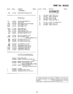
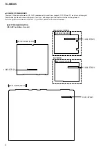
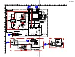
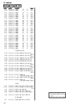
Note on Printed Wiring Boards:
Note:
•
X
: parts extracted from the component side.
•
f
: internal component.
•
: Pattern from the side which enables seeing.
r
Waveforms
• Abbreviation
AUS
: Australian
Summary of Contents for TC-WE305
Page 3: ......
Page 4: ......
Page 5: ......
Page 6: ......
Page 7: ......
Page 8: ......
Page 9: ......
Page 10: ......
Page 11: ......
Page 12: ......
Page 13: ......
Page 14: ... 18 TC WE305 Ver 1 1 2002 10 ...
Page 15: ......
Page 16: ......
Page 17: ......
Page 18: ......
Page 19: ......
Page 20: ......
Page 21: ......
Page 34: ...13 TC WE305 MEMO ...