background image

STR-DN860/DN1060

16

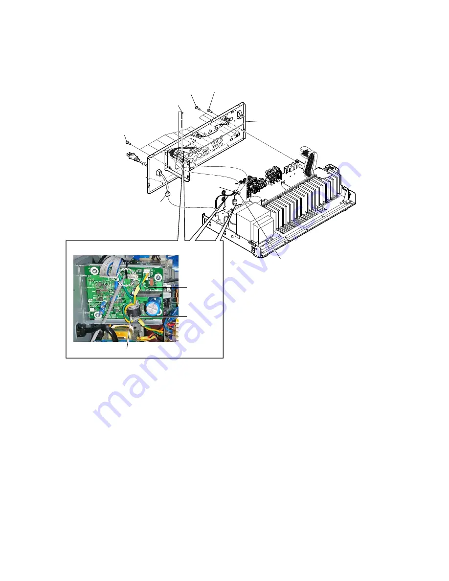
2-9.  BACK PANEL SECTION (DN860)

1

 CNP901

 (3P)

3

 CN1905

 (4P)

4

 CN1907 (2P)

5

 five screws

 (+BVTP 

u

 8)

6

 three screws

 (+BVTP 

u

 8)

6

 eight screws

 (+BVTP 

u

 8)

7

  back panel section

2

  Cut the cable tie

cushion (R)

DCDC board

‡:LUHVHWWLQJ

clamp,
sleeve ferrite

Summary of Contents for STR-DN1060

Page 1: ...he EULA for network services please refer to License agreement in options menu on each network service icon For details of the GPL LGPL and other software licenses please refer to Software License Information in System Settings of the Setup menu on this product This product contains software that is subject to the GNU General Public License GPL or GNU Lesser General Public License LGPL These estab...

Page 2: ... 2 4 GHz 5 GHz BLUETOOTH section Communication system BLUETOOTH Specification version 3 0 Output BLUETOOTH Specification Power Class 1 Maximum communication range Line of sight approx 30 m 98 4 feet 1 Frequency band 2 4 GHz band 2 4000 GHz 2 4835 GHz Modulation method FHSS Freq Hopping Spread Spectrum Compatible BLUETOOTH profiles2 A2DP 1 2 Advanced Audio Distribution Profile AVRCP 1 5 Audio Video...

Page 3: ...for this job 3 Measuring the voltage drop across a resistor by means of a VOM or battery operated AC voltmeter The limit indication is 0 75 V so analog meters must have an accurate low voltage scale The Simpson 250 and Sanwa SH 63Trd are examples of a passive VOM that is suitable Nearly all battery operated digital multimeters that have a 2 V AC range are suitable See Fig A 1 5 kΩ 0 15 μF AC voltm...

Page 4: ...Schematic Diagram MB 1409 Board 11 18 55 6 21 Schematic Diagram MB 1409 Board 12 18 56 6 22 Schematic Diagram MB 1409 Board 13 18 57 6 23 Schematic Diagram MB 1409 Board 14 18 58 6 24 Schematic Diagram MB 1409 Board 15 18 59 6 25 Schematic Diagram MB 1409 Board 16 18 60 6 26 Schematic Diagram MB 1409 Board 17 18 61 6 27 Schematic Diagram MB 1409 Board 18 18 62 6 28 Printed Wiring Board MAIN Board ...

Page 5: ...oard NOTE OF REPLACING THE IC1236 ON THE MAIN BOARD IC1236 on the MAIN board cannot exchange with single When this part on the MAIN board is damaged exchange the entire mounted board MODEL IDENTIFICATION BACK PANEL Model Part No DN1060 US Canadian 4 547 190 0 DN1060 AEP UK 4 547 190 1 DN1060 Australian 4 547 190 2 DN860 US Canadian 4 547 191 0 DN860 AEP UK 4 547 191 1 DN860 Australian 4 547 191 2 ...

Page 6: ...ard used in this unit required to unsolder the grounding wire on the DCDC Board Grounding wire After replaced the IC1906 IC1911 IC1912 IC1913 IC1914 and IC1915 have to solder back the grounding wire on the DCDC Board properly before turn on the set refer image provided below Caution If insufficient solder occured for the grounding wire in DCDC Board it may caused the set intermittent turn on off a...

Page 7: ...nal speaker until you detect which speaker is causing the protection error After checking the above items and fixing any problems plug in the AC power cord mains lead and turn on the receiver If the problem persists consult your nearest Sony dealer An over current from the USB port was detected Disconnect all USB devices as prompted in the warning message and close the message For other messages s...

Page 8: ...e m button on the remote commander to select 6 P2P Registry Check Screen 6 13 Press the button on the remote commander to check the P2P device address is the same as shown in Screen 5 Displayed characters values in the following figure are example 14 Press the RETURN button on the remote commander and select Factory Initialize go to Screen 7 15 The set will turn off automatically Diag Category Blu...

Page 9: ... MB 1409 BOARD DN1060 Page 14 2 5 CARD WLAN BT COMBO DN1060 Page 12 2 3 CASE STEPUP DN1060 Page 10 2 4 CARD WLAN BT COMBO DN860 Page 11 2 6 MB 1409 BOARD DN860 Page 13 2 8 FRONT PANEL SECTION Page 15 2 9 BACK PANEL SECTION DN860 Page 16 2 10 BACK PANEL SECTION DN1060 Page 17 2 11 STANDBY BOARD MAIN BOARD SECTION Page 18 2 12 MAIN BOARD Page 19 SET ...

Page 10: ...e numerical order given 2 2 CASE ENTRY DN860 3 three screws BVTP 3 u 8 4 2 three screws B TYPE 4 u 8 5 case entry 1 three screws B TYPE 4 u 8 4 2 3 CASE STEPUP DN1060 3 four screws BVTP 3 u 8 4 2 three screws B TYPE 4 u 8 5 case stepup 1 three screws B TYPE 4 u 8 4 ...

Page 11: ... cushion R 3 cushion R 8 two screws BVTP 3 u 8 0 one screw BVTP 3 u 8 rear side DCDC board MB 1409 board cable tie clamp cushion R LUH VHWWLQJ Note Process so that lead wire does not contact CN301 and W1990 rear side bracket module bottom cushion R cushion R LUH VHWWLQJ 86 1 1 Wire is removed from the clamp Abbreviation CND Canadian model ...

Page 12: ... 7 bracket module bottom 1 CN502 5P 3 cushion R 2 cushion R 6 two screws BVTP 3 u 8 8 one screw BVTP 3 u 8 Note Process so that lead wire does not contact CN301 and W1990 rear side DCDC board MB 1409 board cushion R rear side bracket module bottom cushion R cushion R LUH VHWWLQJ LUH VHWWLQJ ...

Page 13: ...VTP 3 u 8 qh heat sink HDMI B qj sheet radiation qk MB 1409 board qg heat sink HDMI A H I 1 wire flat type 27 core CN3004 4 wire flat type 19 core CN8001 3 CN8000 13P 2 wire flat type 22 core CN8002 7 six screws B 3 u 5 8 one screw BVTP 3 u 8 9 two screws BVTP 3 u 8 MB 1409 board pin lead pin lead DISPLAY board MB 1409 board pin lead and cable tie LUH VHWWLQJ LUH VHWWLQJ Note Process so that lead ...

Page 14: ...l tape qk rivet DIA 3 nylon w copper shield N106 H J I 3 wire flat type 27 core CN3004 6 wire flat type 19 core CN8001 1 HDMI cable CN3501 5 CN8000 13P 2 CN3500 7P 4 wire flat type 22 core CN8002 9 seven screws B 3 u 5 0 one screw BV 3 u 8 CU US CND one screw BVTP 3 u 8 AEP UK AUS qa two screws BVTP 3 u 8 AEP UK AUS qd one screw BVTP 3 u 8 MB 1409 board DCDC board Note Process so that lead wire do...

Page 15: ...VHWWLQJ LUH VHWWLQJ 2 Wire is removed from the pin lead 3 cushion R 4 CN1391 4P 7 front panel section 5 five screws BVTP 3 u 8 6 one screw BVTP 3 u 8 6 one screw BVTP 3 u 8 5 two screws BVTP 3 u 8 rear side rear side 1 Cut the cable tie 1 Cut the cable tie DN1060 DN1060 DN1060 DN1060 DN1060 DN1060 DN1060 DN1060 DN1060 DN860 MAIN board POWERKEY board pin lead rear side ...

Page 16: ...K PANEL SECTION DN860 1 CNP901 3P 3 CN1905 4P 4 CN1907 2P 5 five screws BVTP 3 u 8 6 three screws BVTP 3 u 8 6 eight screws BVTP 3 u 8 7 back panel section 2 Cut the cable tie cushion R DCDC board LUH VHWWLQJ clamp sleeve ferrite ...

Page 17: ...AUS Australian model CND Canadian model 1 CNP901 3P 2 CN1905 4P 3 CN1907 2P 4 seven screws BVTP 3 u 8 4 eight screws BVTP 3 u 8 5 four screws BVTP 3 u 8 US CND four screws BV RING AEP UK AUS 6 back panel section cushion R DCDC board LUH VHWWLQJ clamp sleeve ferrite ...

Page 18: ...crews BVTP 3 u 8 9 MAIN BOARD section 8 one screw BVTP 3 u 8 2 four screws BVTP 3 u 8 3 STANDBY board 1 CNP902 4P 5 CNP920 5P 6 CNP930 5P 4 Wire is removed from the pin lead LUH VHWWLQJ pin lead MAIN board rear side 2 11 STANDBY BOARD MAIN BOARD SECTION ...

Page 19: ...IN board 0 Remove the forty two solders 1 one screw BVTP 3 u 8 2 INSULATION board 4 USB INSULATION board 3 one screw BVTP 3 u 8 7 one screw BVTP 3 u 8 7 one screw BVTP 3 u 8 8 bracket HDMI support 7 one screw BVTP 3 u 8 5 two screws BVTP 3 u 8 6 SUPPORT board 8 bracket support beam 8 bracket support beam DN1060 DN1060 DN1060 DN1060 DN1060 DN860 ...

Page 20: ...hecked Procedure 1 While pressing SPEAKERS and PURE DIRECT buttons simultaneously press the 1 button to turn on the main power 2 The message REST 12 appears Every pressing of any button other than the 1 counts down the buttons 3 The buttons which are already counted once are not counted again 4 When all buttons are pressed REST 00 appears SWAP ALL MODE The signal will be swap to all channels so th...

Page 21: ... Treble H T x x x Front Level F x x x x x x Center Level C x x x x x x Surround Level S x x x x x x Surround Back Level B x x x x x x Front Height Level H x x x x x x Temperature T E M P Total Power On T x x x x x H x x M Main Power On M x x x x x H x x M Power On Count R E B O X x x MHL VBUS MODE This mode is to display the MHL VBUS status Procedure 1 Press the 1 button to turn on the main power ...

Page 22: ...Performs unit test of devices installed on the board Log Error log is displayed Displayed contents can also be saved in an USB memory device Factory Initialize Restores the unit to its factory settings Network Not used Version Up Not used System Information Displays the system information of the unit Displays information such as the software version drive information etc EMC Test Mode Not used Dri...

Page 23: ... udio Input Test Not used LUHOHVV 1 7HVW 3 3 WHVW RQO 0 7HVW 0RGH Not used Drive Not used 5 7HVW 0RGH Not used Start Initialize QLWLDOL H GHIDXOW VHWWLQJ IRU WKH XQLW LDJ 7HVW Transcoder Test Not used 0 QSXW 7HVW Not used OXHWRRWK HYLFH 7HVW 0LF 7HVW Not used 0RGH Not used Not used Service 0ode 0enu 1 DiaJ LoJ 3 Factory Initialize 4 Network 5 Version Up 6 System Information Service 0ode 0enu 1 Dia...

Page 24: ... Mode 8 Drive Not Support In This Model 9 HDD mode 10 RF Test Mode HELP DOWN ENT 4 Diag Device Test This screen is used to test devices mounted on the board Screen 1 Selects the test category Operation Selects the category m Moves to the selected category RETURN Returns to the service top menu Screen 2 Device test Selects the device to test after selecting Device Test in screen 1 Operation Selects...

Page 25: ...essPoint 3 Start Display RSSI Value 4 Start Ping Test 5 Write P2P address to Registry 6 P2P Registry Check P2P device address xx xx xx xx xx xx HELP UP DOWN ENT RET Screen 1 Screen 2 Screen 3 6 Diag MIC Input Test This screen performs MIC input test Note Not used for the servicing 7 Diag HDMI Input Test This screen performs HDMI input test Note Not used for the servicing 8 Diag Transcoder Test Not...

Page 26: ...ves to the next page RETURN Returns to the screen Screen 1 that selects the log type RED Writes the log contents to an USB memory device Viewing the log display Error Log 174 2010 01 01 00 00 08 ErrCode 0902A4053002 Index number Date Time Error code About copying log to USB memory device Press the RED button in each log display screen with the USB memory device inserted into the unit Note Please d...

Page 27: ...s system information Screen 1 Basic Information Operation Basic Information displayed go to Screen 2 RETURN Returns to service top menu Screen 2 Basic Information continue Operation Basic Information displayed go to Screen 1 RETURN Returns to service top menu When delta IOP is measured it becomes impossible to use the Version Up function Contents List Main LSIname Model Destination Sequence Number...

Page 28: ...75 kHz Modulation 1 kHz ANT input 35 dBu EMF Note Use 75 ohm coaxial cable to connect signal generator and the set You cannot use video cable for checking Use signal generator whose output impedance is 75 ohm 3 Set to FM tuner function and scan the input FM signal with automatic scanning 4 Confirm that input frequency of A B and C are detected and automatic scanning stops When the station signal i...

Page 29: ...ower transistor example Q1600 on the MAIN board the power amplifier and the surrounding circuit are not defect Check that the surrounding circuit of current detect example Q1600 and Q1601 on the MAIN board is not defect Check the surrounding circuit of protector example Q1604 on the MAIN board and exchange the defective parts Check that between the 59 V line 59 V B line and the ground does not sho...

Page 30: ...pins MB 1409 board IC6002 pin 16 19 20 21 Check the following parts and the surrounding circuit and exchange the defective parts MB 1409 board IC3002 IC6500 IC6501 Check the following parts and the surrounding circuit and exchange the defective parts MB 1409 board IC3002 IC6000 Check the following parts and the surrounding circuit and exchange the defective parts MB 1409 board IC3002 MAIN board IC...

Page 31: ... and exchange the defective parts MAIN board IC1230 IC1231 MB 1409 board IC6002 Check the following parts and the surrounding circuit and exchange the defective parts MB 1409 board IC6000 Check that OPT is displayed on the fluorescent indicator Check the following parts and the surrounding circuit and exchange the defective parts MAIN board IC1414 J1401 J1402 Check that the sound from the optical ...

Page 32: ...1913 IC1914 IC1915 IC1906 F940 Check the following parts and the surrounding circuit and exchange the defective parts MB 1409 board IC3700 Check the following parts and the surrounding circuit and exchange the defective parts MB 1409 board IC3001 IC3002 Check the following parts and the surrounding circuit and exchange the defective parts MB 1409 board X3000 Check that voltage of the following pin...

Page 33: ...heck that the speaker pattern setting is normal Explain the settings of this unit to the customer Check the surrounding circuit of power transistor of the channel to which data is not outputted example Q1600 on the MAIN board and the surrounding circuit of power amplifier circuit example FL FR on the MAIN board and exchange the defective parts OK NG NG ...

Page 34: ...N 6 DIAGRAMS Circuit Boards Location STANDBY board DCDC board card WLAN BT COMBO MB 1409 board MAIN board NFC ICON board RC S730 WW POWERKEY board GND BRACKET board HP board FRONTJACK board DISPLAY board FRONT HDMI board DN1060 ...

Page 35: ...WIN 1 OUT1 LINE AMP IC1413 51 6 2 1 52 7 R ch SW C SYSTEM CONTROLLER IC3002 1 4 142 TUNER_MOSI 16 X1 17 X2 143 TUNER_CLK EVOL_DATA DA CL EVOL_CLK 55 56 ZONE2_PREOUT_SW_RY 81 42 43 1 2 44 45 57 9 8 11 10 SUBR 25 SBL 12 R ch R ch C R ch 13 OUTSBL OUTSBR 15 R ch 14 31 32 38 39 36 37 56 AUDIO AMP IC1101 R ch R ch R ch R ch R ch R ch R ch INL6 INR6 34 35 R ch R ch R ch 7 5 1 3 12 LRCK LOUT 13 DA 11 CK ...

Page 36: ...1 BINARY COUNTER IC6004 MUTE SELECTOR IC6005 SD RAM IC6500 D6003 D501 FS_RATE 1CK 2QD 88 6LJQDO SDWK AUDIO AUDIO DIGITAL 5 FK LV RPLWWHG GXH WR VDPH DV FK 5 2 3 6 MCKOUT 13 MCLK_IN 92 LRCKOUT 15 LRCLK_IN 97 BCKOUT 14 BCLK_IN 75 MUTEB MCKOUT 13 XMCK 30 24 B Y SELECT 2 5 A 1 6 MPIN5 11 MCKOUT 13 BCKOUT 14 ARC_SPDIF CEC_PCONT V_COM_MUTE V_SEL_MUTE V_SEL_SW2 SIGNAL SELECTOR MUTING IC6003 SRC IC6007 8 ...

Page 37: ...AL SIGNAL PROCESSORS AND CONTROLLERS IC7100 H22 H23 J22 J23 K22 K23 L22 L23 K20 J20 L20 16 A6 122 SCK0 DDCK C6 125 MCLK D6 130 SPDIF0_OUT DL2 B4 DATA2 DATA2 DATA1 DATA1 DATA0 DATA0 CLOCK CLOCK SCL 5V SDA 5V HOT PLUG DET CEC 5V POWER R1X2 R1X1 R1X1 R1X0 R1X0 R1XC R1XC DSCL1 26 25 24 23 22 21 20 81 DSDA1 CBUS_HPD1 80 82 RX2N RX1P RX1N RX0P RX0N RXCP RXCN DSCL 15 14 13 12 11 8 7 75 DSDA RX_HPD 76 4 1...

Page 38: ...5 SL LIMITER Q1552 Q1553 BOOSTER Q1550 CURRENT DETECT Q1554 CURRENT DETECT Q1555 BOOSTER Q1551 LIMITER Q1602 Q1603 BOOSTER Q1600 CURRENT DETECT Q1604 CURRENT DETECT Q1605 BOOSTER Q1601 SYSTEM CONTROLLER IC3002 3 4 C PROTECT TEMP_SENSOR1 TEMP_SENSOR3 LIMITTER HP_RY FRONT_SPK_RY SBL_SBR_RY C_RY HP_DET LIMITER Q1802 Q1803 BOOSTER Q1800 CURRENT DETECT Q1804 CURRENT DETECT Q1805 PROTECTOR Q1320 Q1321 Q...

Page 39: ... 5 VIN3 3 VIN2 1 VIN1 7 POWER SAVE 4 SW2 6 MUTE 5 VIN3 VIN2 3 J1202 DN860 J1201 2 2 DN1060 J503 6 RX RX TX TX 3 2 1 VIDEO MONITOR OUT COMPONENT VIDEO SAT CATV ASSIGNABLE IN VIDEO VIDEO IN VIDEO VIDEO 1 IN VIDEO SAT CATV IN VIDEO MONITOR OUT VIDEO SAT CATV IN MONITOR OUT 8 VOUT BD DECODER IC101 2 3 AC28 TXVP_1 AC27 TXVN_1 AB27 TXVN_0 AB28 TXVP_0 B4 USB_DM_P1 A4 USB_DP_P1 AA28 USB_DM_P2 AA27 USB_DP_...

Page 40: ...6 86B 3 84 86 R3PWR5V 91 BUFFER CEC 63 57 B567 5 B5 B567 R0PWR5V 79 0 75 16 9 5 IC3700 2 2 BD DECODER IC101 3 3 DATA2 DATA2 DATA1 DATA1 DATA0 DATA0 CLOCK CLOCK 6 9 6 9 HOT PLUG DET CEC 5V POWER 17 16 15 14 13 12 11 10 77 76 78 RX2P 16 HDMI RECEIVER IC5001 R5PWR5V 100 6 1 6 725 MULTIPLEXER DEMULTIPLEXER IC5018 2 2 EEPROM IC5000 6 1 8 5 IC4020 54 R4X2 40 TXCN C27 16B 7 A3 6 B3 6 46 TX2N 47 TX2P 75 6...

Page 41: ...101 LED DRIVER Q1102 LED PURE DIRECT D1108 LED DRIVER Q1110 LED DRIVER Q1111 LED ON STBY D1110 AC OFF DETECT Q952 49 FL_ENABLE 73 POWER_RY 62 PURE_DIRECT_LED 124 FLASH_CLK PWR_LED 61 STANDBY_LED 2 5V REG IC1913 14 SW2 1 3 SW1 VIN1 16 VIN2 75 AC CUT 79 BRIDGEABLE_RY 42 40 38 51 FL_LAT 60 FL_CLK 59 FL_DATA 93 VOLUME_JOG 90 INPUT_JOG 58 POWER_KEY 91 AD_KEY1 92 AD_KEY2 86 X0 CLOCK IN 87 X1 SWITCHING T...

Page 42: ... une piéce portant le nu méro spécifié Caution Pattern face side Conductor Side Parts face side Component Side Parts on the pattern face side seen from the pattern face are indicated Parts on the parts face side seen from the parts face are indicated HDMI board and DSP board are multi layer printed board However the patterns of intermediate layers have not been included in diagrams Indication of t...

Page 43: ...8 R6024 CL7040 R515 R6025 CL7041 R6026 CL7042 R6027 CL7043 FB3824 CL7044 C6050 FB3825 R6029 CL7045 C6051 C3941 C6052 CL7046 C6053 CL7047 R3727 R328 2 1 7 6 CN7000 C6054 CL7048 1 5 6 7 CN501 R329 CL7049 CN502 R6030 R6031 R6033 R330 R6034 CL7050 R331 CL7051 R5289 CL7052 R5096 R3732 CL7053 R3733 R6037 R5098 CL7054 R6038 CL7055 R3735 R6039 R336 C6062 CL7056 R3736 CL7057 R3737 CL7058 R3738 CL7059 R3739...

Page 44: ...013 R3533 R327 JL2014 R3534 C3750 R3728 JL2015 C6055 R3535 R3729 C3751 JL2016 R3536 C6056 C3752 JL2017 R3537 C6057 C3753 JL2018 R3538 C3754 R3539 R5091 C6059 C3755 R6032 C3756 C3757 C3758 R3730 C101 R6035 R3731 C3759 R332 C102 R6036 C103 C104 C7000 R3734 R3540 C7001 R3541 C106 C7320 R3542 C7003 R3543 C6063 C7004 L3810 R3544 C3760 C6064 C7005 C3761 C6065 C7006 C3762 C7007 R530 C7008 R531 C7009 R532...

Page 45: ...101 0 1u C180 0 1u C181 0 1u C182 0 1u C137 10u C156 10u C175 4p C178 100p C177 4p C176 100p C179 0 1u C121 0 01u C118 0 1u C115 0 1u C106 0 1u CL107 CL108 CL109 CL112 CL113 CL114 CL115 CL116 CL117 CL118 CL120 CL121 CL2118 CL123 CL124 CL125 CL126 CL127 CL128 CL129 CL130 CL131 CL132 CL133 CL134 CL135 CL2101 CL2102 CL2103 CL2104 CL2105 CL2106 CL2117 CL2116 CL122 CL2115 CL2114 CL2113 CL2112 CL2111 CL...

Page 46: ...C_28 29 I O1 30 I O2 31 I O3 32 I O4 33 NC_33 34 NC_34 35 NC_35 36 VSS_36 37 VCC_37 38 NC_38 39 NC_39 40 NC_40 41 I O5 42 I O6 43 I O7 44 I O8 45 NC_45 46 NC_46 47 NC_47 48 NC_48 GND GND NAND FLASH IC2001 FLASH IC101 2 15 CXD90028GB B EXCEPT TW CXD90028GB C TW BD DECODER IC101 IC101 5 15 CXD90028GB B EXCEPT TW CXD90028GB C TW BD DECODER IC101 IC101 6 15 CXD90028GB B EXCEPT TW CXD90028GB C TW BD DE...

Page 47: ... 5 2V REG IC302 1u C329 2 2u C330 DSP_1 1V 10k R348 3 9k R379 220 R380 10k R349 BD00IC0WHFV GTR IC313 VO 1 FB 2 GND 3 EN 4 NC 5 VCC 6 7 JL318 1 1V REG IC313 1u C319 1u C320 6 3V 220u C364 MTKSTB_3 3V 10k R328 22k R330 10k R331 10k R329 BD00IC0WHFV GTR IC308 VO 1 FB 2 GND 3 EN 4 NC 5 VCC 6 7 JL314 3 3V REG IC308 1u C303 1u C304 6 3V 220u C365 MTK_3 3V 10k R302 22k R304 10k R305 10k R303 BD00IC0WHFV...

Page 48: ...45 JL444 JL443 JL442 JL417 JL440 JL439 JL438 JL437 JL415 JL435 JL419 JL447 JL446 0 R466 10k RB401 R419 100 100 R423 0 1u C402 R431 100 R430 100 R418 100 R428 JL424 10k R429 JL425 JL422 JL423 JL426 10k 0 R452 R465 2 2k R462 2 2k R463 2 2k RB402 10k R432 1k R427 10k 10k R467 10k R468 100 R420 100 R421 0 R472 0 R470 R443 0 820 R478 100 R475 100 R474 100 R476 1M R477 R473 10k IF_SDO STRAP_XAMUTE IF_SD...

Page 49: ...u C538 6 3V 220u C534 CL513 CL514 5P CN501 1 2 3 4 5 5P CN502 1 2 3 4 5 ET502 ET501 MTK_3 3V USB_5 2V USB_RF_5 2V MTK_3 3V MTKSTB_3 3V MTKSTB_3 3V J503 8P 1 2 3 4 5 6 7 8 JL503 JL504 JL501 JL507 JL506 0uH L502 0uH L501 1k R538 10k R532 10k R533 10k R537 75 RB501 10k R534 10k R535 0 R507 10k R531 0 R508 0 R515 WLAN BT COMBO CARD 1k R530 24k R518 5 1k R505 5 1k R504 0 R514 USB_PCONT WIFI_PCONT OCPI ...

Page 50: ...2 DGND12_K N12 DGND12_K P12 DGND12_K R12 DGND12_K T12 DGND12_K U12 DGND12_K V12 DGND12_K AB12 DGND12_K J13 DGND12_K K13 DGND12_K L13 DGND12_K M13 DGND12_K N13 DGND12_K P13 DGND12_K R13 DGND12_K T13 DGND12_K U13 DGND12_K V13 DGND12_K L14 DGND12_K M14 DGND12_K N14 DGND12_K P14 DGND12_K R14 DGND12_K G14 DVCC33_IO_1 H14 DVCC33_IO_1 G8 DVCC33_IO_2 H8 DVCC33_IO_2 U21 DVCC33_IO_4 V21 DVCC33_IO_4 G22 DVCC...

Page 51: ...DD12OUT 57 HSIC_VDD33 58 HSIC_VDD10 59 VDD10_59 60 SPI_CLK 61 SPI_CS0 62 SPI_CS1 63 SPI_MOSI 64 SPI_MISO 65 VDDIO33_65 66 TDSCL 67 TDSDA 68 CSCL 69 CSDA 70 VDD10_70 71 MHL_CD 72 NC_72 73 WAKEUP 74 LPSBV5V 75 DSCL 76 DSDA 77 CN5001 19P 1 DATA2 2 DATA2 SHIELD 3 DATA2 4 DATA1 5 DATA1 SHIELD 6 DATA1 7 DATA0 8 DATA0 SHIELD 9 DATA0 10 CLOCK 11 CLOCK SHIELD 12 CLOCK 13 CEC 14 RESERVE NC 15 SCL 5V 16 SDA ...

Page 52: ...SIC_STB 55 HSIC_GND 56 VDD12OUT 57 HSIC_VDD33 58 HSIC_VDD10 59 VDD10_59 60 SPI_CLK 61 SPI_CS0 62 SPI_CS1 63 SPI_MOSI 64 SPI_MISO 65 VDDIO33_65 66 TDSCL 67 TDSDA 68 CSCL 69 CSDA 70 VDD10_70 71 MHL_CD_TX 72 RSVDL_72 73 NC_73 74 LPSBV5V 75 DSCL 76 DSDA 77 12 5 C5072 220u 6 3V 13 100 R5155 MHLDCDC_6 2V CN5005 7P 1 3 3V 2 GND 3 Rogue_RxD 4 NC 5 Rogue_TxD 6 NC 7 NC 10 R5178 C5184 0 1u CN5012 19P 1 DATA2...

Page 53: ...0 5V_SP 0uH FB3500 IN2_D0 IN2_D1 IN2_D1 IN2_D2 IN2_D2 15 17 10k R3508 DA_3 3V MHL0_PCONT 33 34 35 36 37 38 39 40 41 42 43 44 45 46 47 48 0 1u C3927 10k R3572 0 1u C3928 S2 SDA I2C_SEL HPD1 SDA1 SCL1 CLK _1 CLK _1 VCC_40 D0 _1 D0 _1 GND_43 D1 _1 D1 _1 VCC_46 D2 _1 D2 _1 TMDS261BPAGR IC3821 1 2 3 4 5 6 7 8 9 10 11 12 13 14 15 16 NC_1 NC_2 GND_3 NC_4 NC_5 VCC_6 NC_7 NC_8 GND_9 NC_10 NC_11 VCC_12 NC_1...

Page 54: ...1 177 GND 158 159 160 161 162 163 164 165 166 167 168 169 170 171 172 173 174 175 176 140 141 142 143 144 145 146 147 148 149 150 151 152 153 154 155 156 157 133 134 135 136 137 138 139 D0 D1 D2 D3 D4 D5 D6 D7 D8 D9 D10 IDCK IOVCC33 D11 D12 D13 ARC0 ARC1 CVCC12 TPVDD12 TDVDD12 T1XC T1XC T1X0 T1X0 T1X1 T1X1 T1X2 T1X2 TPVDD12 TDVDD12 T0XC T0XC T0X0 T0X0 T0X1 T0X1 T0X2 T0X2 CVCC12 SD0_IN SPDIFO_IN SC...

Page 55: ... 100 R3062 2 2k R3016 100 R3017 100 R3018 100 R3019 100 R3020 47 R3075 100 R3021 100 R3080 100 R3022 100 R3081 100 R3023 100 R3083 2 2k R3132 100 R3086 100 R3087 100 R3090 100p C3016 100p C3017 2 2k R3092 2 2k R3089 100 R3103 2 2k R3125 2 2k R3126 100 R3098 1k R3111 470 R3120 100 R3110 470 R3119 1M R3129 1M R3130 1M R3131 R3108 100 100 R3058 100 R3045 10k R3121 10k R3122 10k R3123 10k R3124 100 R3...

Page 56: ...94 330 R6013 330 R6026 100 R6001 0 R6052 47 R6033 100 R6053 47k R6048 1k R6049 100 R6031 100 R6037 470 R6017 47 R6015 R6030 100 330 R6016 1M R6000 470p C6004 22k R6010 33k R6011 100 R6022 330 R6023 100 R6002 10k R6063 75 R6027 1k R6003 220 R6012 100 R6059 0 R6061 470 R6007 0 R6050 1M R6024 47 R6062 10k R6032 470k R6009 10k R6029 47 R6014 680 R6025 R6095 100 47k R6008 0 R6055 100 R6038 100 R6040 10...

Page 57: ...K IC6009 SELECT 1 1A 2 1B 3 1Y 4 2A 5 2B 6 2Y 7 GND 8 3Y 9 3B 10 3A 11 4Y 12 4B 13 4A 14 ST 15 VCC 16 TC74VHC157FT EK IC6008 SELECT 1 1A 2 1B 3 1Y 4 2A 5 2B 6 2Y 7 GND 8 3Y 9 3B 10 3A 11 4Y 12 4B 13 4A 14 ST 15 VCC 16 SRC4190IDBR IC6007 LGRP 1 RCKI 2 NC 3 SDIN 4 BCKI 5 LRCKI 6 VIO 7 DGND_8 8 BYPAS 9 IFMT0 10 IFMT1 11 IFMT2 12 RST 13 MUTE 14 RDY 15 OWL1 16 OWL0 17 OFMT1 18 OFMT0 19 TDMI 20 DGND_21 ...

Page 58: ...7 FRONTHI_L R_OUT 78 VDD_INT 79 NC 80 NC 81 NC 82 NC 83 NC 84 VDD_EXT 85 VDD_INT 86 L R_OUT 87 MID SW2_OUT 88 SBL SBR_OUT 89 ZONE_L R 90 VDD_INT 91 VDD_EXT 92 MCLK_IN 93 VDD_INT 94 C SW1_OUT 95 C SW_IN 96 A D_2CH 97 LRCLK_IN 98 BCLK_OUT 99 LRCLK_OUT 100 L R_IN 101 SBL SBR_IN 102 VDD_INT 103 DIR_IN 104 VDD_EXT 105 VDD_INT 106 BOOT_CFG2 107 VDD_INT 108 AMI_ACK 109 GND 110 THD_M 111 THD_P 112 VDD_EXT...

Page 59: ...05 0 1u C7004 0 1u C7003 1u C7002 1u C7001 10u C7000 10u C7490 10u C7491 10u C7492 10u C7493 10u 0 15u C7156 0 012u C7157 0 012u C7155 0 15u C7154 ADV_1 8V 5V_SP FB7000 0uH 47k R7128 1 8k R7122 1 8k R7120 R7154 150 1k R7143 0 R7140 R7145 1k R7144 1k R7141 0 R7142 0 R7155 22 R7156 150 R7157 22 22 R7123 0 R7129 22 R7121 470 R7131 0 1u C7131 4 7k R7510 4 7k R7511 4 7k R7100 4 7k R7101 4 7k R7102 4 7k...

Page 60: ...00 JL7701 JL7702 JL7703 JL7704 JL7705 JL7706 JL7707 JL7708 JL7709 JL7710 JL7723 JL7725 DDR2_1 8V FB7207 0uH FB7200 0uH FB7400 0uH JL7400 R7219 22 R7220 22 R7223 22 R7221 22 R7400 1k R7401 1k R7239 47 R7238 47 R7216 47 R7218 47 R7241 47 R7226 22 R7236 47 R7235 47 R7288 47 R7290 47 R7291 47 R7289 47 R7285 47 R7284 47 R7286 47 R7287 47 R7281 47 R7280 47 R7283 47 R7282 47 R7276 47 R7279 47 R7278 47 R7...

Page 61: ...2 CL7023 CL7038 CL7039 CL7031 CL7036 CL7029 CL7034 CL7028 CL7021 CL7026 JL7735 JL7739 JL7740 JL7741 JL7742 JL7743 JL7726 JL7727 JL7728 JL7729 JL7730 JL7731 JL7711 JL7712 JL7713 JL7714 JL7715 JL7716 JL7717 JL7734 JL7718 JL7719 JL7720 JL7721 JL7722 JL7724 JL7732 JL7733 DA_3 3V DA_3 3V ADVETH_1 8V FB7300 0uH FB7302 0uH FB7303 0uH FB7304 0uH FB7305 0uH FB7301 0uH JL7304 JL7303 JL7483 JL7371 JL7370 JL7...

Page 62: ...ZONE2_PREOUT_SW_RY 10 SBL_SBR_RY 11 BRIDGEABLE RY 12 HP_RY 13 TEMP_SENSOR_1 14 TEMP_SENSOR_2 15 LIMITER 16 TEMP_SENSOR_3 17 NC 18 NC 19 NW_LCH_N AGND 20 NW_LCH_P NW_ZONE2_L 21 NW_RCH_P AGND 22 NW_RCH_N NW_ZONE2_R BAV70 D501 USBDCDC_6 2V A_ 5V DA_3 3V 7V FB8000 0uH FB8002 0uH 0uH FB8001 22 R8022 22 R8021 22 R8019 22 R8020 22 R8023 22 R8024 22 R8025 22 R8026 100 R8000 47k R8002 10k R8016 22k R8004 1...

Page 63: ...16 R1623 R1817 R1624 R1625 JW1301 R1626 JW1302 21 6 10 16 20 1 5 11 15 IC1236 R1627 JW1303 IC1237 R1628 D1820 L1700 R1629 D1821 D1822 C1653 Q1650 R1820 C1655 Q1651 R1821 Q1652 E R1822 Q1653 E R1823 C1658 R1630 R1824 IC1240 C1270 R1825 ET1301 R1826 R942 C1272 R1827 R943 R1634 R1828 R944 C1274 R1635 R1829 TB1501 C1853 R1637 R947 R1250 Q1850 R1638 Q1851 R1251 R1639 C1662 Q1852 E R1252 R1253 Q1853 E C...

Page 64: ...5 CL1651 C1216 CL1652 C1218 C1601 C1604 C1606 CL1850 Q1604 CL1851 Q1605 CL1852 CL1853 C1224 C1225 C1801 C1226 C1227 C1804 C1229 C1805 C1806 JL1260 Q1804 JL1261 Q1805 JL1262 C1422 JL1263 C1424 C1426 C1233 C1428 C1236 C1237 R1403 C1238 R1212 R1407 R1214 R1408 D1600 R1215 D1601 R1217 R1218 C1628 R1602 R1411 R1412 R1607 D1800 R1609 D1801 R1224 C1828 IC1410 R1225 IC1411 R1226 IC1412 R1802 IC1413 CC1001...

Page 65: ...5 15k R1864 68k R1869 47k R1868 100k R1859 47k R1857 R1481 0 22 C1878 0 022u SBR VE SBR VE B C E E B C C1801 220p C1804 0 01u C1841 47p C1842 47p C1808 47u 25V CL1800 CL1801 CL1802 R1803 0 22 D1800 DA2J10100L D1801 DA2J10100L L1800 Q1801 MP1620 OPY MK BOOSTER Q1800 MN2488 OPY MK BOOSTER Q1805 MSB92T1G CURRENT DETECT Q1802 2SA1162 G LIMITER Q1804 MSB92T1G CURRENT DETECT Q1803 2SD2114K LIMITER R1808...

Page 66: ...5 2SC2713 G PROTECTOR Q1321 2PD601ART PROTECTOR Q1324 2PD601ART PROTECTOR 1k R1328 6 8k R1325 10k R1327 CL1868 39k R1326 220 R1449 220 R1450 22k R1320 22k R1323 TH1253 10k R1252 2 2k TH1252 10k R1251 2 2k C1250 0 1u TH1251 10k CL1395 CN1003 22P 1 NW_RCH_N NW_Z2_R 2 NW_RCH_P AGND 3 NW_LCH_P NW_Z2_L 4 NW_LCH_N AGND 5 NC 6 NC 7 TEMP SENSOR3 8 LIMITER 9 TEMP SENSOR2 10 TEMP SENSOR1 11 HP RY 12 BRIDGEA...

Page 67: ... IC1412 NJM4565M TE2 OUT1 1 1 VSS 2 2 OUT2 VCC J1402 6P J1401 6P JW1301 Q1301 2PD601ART RELAY DRIVER Q1302 2PD601ART RELAY DRIVER R1303 33 R1302 100 15k R1584 15k R1784 820 R1683 820 R1633 820 R1833 820 R1783 C1506 270p 15k R1534 820 R1533 820 R1583 22 R1312 22 R1310 22 R1311 22 R1313 1k R1301 1k R1306 15k R1834 1k R927 1k R928 1k R1403 1k R1453 1k R1407 1k R1457 1k R1408 1k R1458 1k R1411 1k R141...

Page 68: ... 10 CC1014 0 01u RR1014 10 CC1017 0 01u RR1017 10 CC1018 0 01u RR1018 10 RR1012 10 RR1011 10 CC1013 0 01u RR1013 10 R920 33 R1361 33 2 2k R921 2 2k R1360 47k R1363 47k R925 RY1360 12V 1 2 3 4 5 6 RY920 12V 1 2 3 4 5 6 7 8 TB1503 4P TB1502 4P TB1501 6P 1 2 3 4 5 1 2 3 4 5 1 2 3 4 5 6 7 8 W1001 1 B FL V RY 2 PROTECTOR 3 ACLASS 4 SBL SBR 5 SR SL 6 C 7 FL FR 8 CHASIS 9 PHASE 10 DIG 7V FR FL C_GND SB_G...

Page 69: ...DRF 6 IIC RDSI 7 LA 21 C1221 10p L1203 47nH 100 R1216 L1202 47nH C1243 10u C1244 10u R1200 1k R1201 1k TUNER_L LRCK TUNER_R BCK 7V TUNER_GND L1201 22nH C1202 1u D1200 BAV99 215 CL1200 C1209 0 0022u CL1201 22 R1206 100 R1207 C1208 4p C1219 4p C1220 0 0033u 0 R1208 CN1200 2P 1 RF GND 2 RF C1230 68p 22 R1205 C1222 0 047u 10k R1209 10k R1204 C1206 10u TUNER_CK TUNER_IIC RDS TUNER_DA TUNER_CE J1202 3P ...

Page 70: ...1142 CL1133 CL1131 CL1145 CL1146 CL1132 CL1143 CL1134 CL1141 CL1144 CL1139 CL1140 Q1102 E D1107 CL1148 CL1147 C1119 C1121 C1122 C1125 C1126 C1128 C1129 C1130 C1132 C1133 C1134 C1135 C1136 C1138 C1139 C1142 C1143 C1115 C1114 D1105 A K FB1100 FB1101 R1113 R1114 R1115 R1116 R1117 R1118 R1119 R1121 R1122 R1123 R1124 R1125 R1126 R1127 R1128 R1129 R1130 R1131 R1132 R1133 R1134 R1135 R1136 R1137 R1138 R1...

Page 71: ...5 IC1101 NJM2904M 1 A_OUTPUT 2 A INPUT 3 A INPUT 4 GND B INPUT 5 B INPUT 6 B_OUTPUT 7 V 8 T1100 TRANSFORMER DC CONVERTER 1 2 4 5 6 7 8 9 3 100 R1141 C1136 0 1u C1139 0 1u C1138 0 1u C1126 0 1u C1143 0 1u CL1139 CL1140 CL1141 CL1142 CL1143 CL1144 CN1103 7P 1 STBY_3 3V 2 NFC_SCL 3 DGND 4 NFC_SDA 5 NFC_IRQ 6 NFC_RFDET 7 NC CL1128 CL1127 CL1126 CL1125 CL1124 CL1123 CL1130 CL1129 CL1121 CL1120 CL1119 C...

Page 72: ... C1976 C1977 C1978 C1979 C1981 C1983 C1984 C1985 C1986 C1987 C1988 C1989 C1990 C1991 C1992 C1993 C1994 C1995 C1996 C1997 C1998 C1999 R1973 R1974 R1975 R1977 R1979 F940 W1901 LP1902 FB1901 FB1902 FB1903 FB1904 FB1905 FB1906 FB1907 L1914 L1917 L1919 L1920 L1921 L1925 L1929 L1930 L1931 L1933 L1934 L1935 L1936 L1937 L1938 D906 K A CL1940 CL1941 CL1942 CL1943 CL1944 CL1947 CL1948 CL1949 CL1950 CL1951 C...

Page 73: ...470u 10V C1966 470u 10V C1967 100p CL1951 4 7 R1915 47k R1923 10k R1922 C1907 22u C1908 22u C1962 0 1u C1919 0 001u 1 EN 2 FB 3 VREG 4 SS 5 GND 6 SW 7 BOOT 8 VIN 9 10k R1927 L1925 2 2uH 2 2k R1928 C1955 10u C1922 10u C1957 10u C1961 0 1u C1959 0 0033u C1986 1u L1937 4 7uH C1916 0 1u C1969 100p IC1911 TPS54394 PWPR 1 VIN1 2 VBST1 3 SW1 4 PGND1 5 EN1 6 PG1 PG1 PG2 PG2 7 VFB1 8 GND VREG5 9 VFB2 10 11...

Page 74: ...972 D992 K A K A D994 T902 JS901 D991 A K Q951 E E Q952 E CL901 Q953 R960 R961 R963 R973 R974 R981 R982 R984 C960 C961 C962 D905 A KA K D901 A K A K A K A K D902 D903 D904 C971 CL906 CL907 CL905 CL903 CL902 CL904 STANDBY BOARD COMPONENT SIDE 1 893 867 11 11 1 893 867 11 11 POWER TRANSFORMER SUB DCDC BOARD CN1905 Page 72 014P MAIN BOARD CNP920 Page 63 009P MAIN BOARD CNP930 Page 63 010P T901 POWER ...

Page 75: ...1 47 R972 33 10k R963 10k R961 100 R974 47k R973 4 7k R960 RY951 CN940 5P 1 STBY 10V 3 STBY GND 4 AC CUT 5 PWR RY Q953 CL902 CL904 CL903 2PD601ART RELAY DRIVER Q951 2PD601ART RELAY DRIVER 220 R982 4 7k R981 C970 50V 10u C971 0 1u 10k R984 D992 RB521SM 30GJT2R D994 CES521 GS1G D904 GS1G D902 GS1G D903 GS1G POWER TRANSFORMER MAIN T901 AC IN 069S MAIN BOARD 4 5 CNP920 Page 68 062S MAIN BOARD 2 5 CNP9...

Page 76: ...RD 5 18 CN501 Page 49 100 R1193 C1154 0 22u 1 A B C D E F 2 3 4 5 6 7 8 ET1101 1 5 CN1104 5 6 7 1 4 CN1106 C1151 J1100 1 3 CN1105 D1130 D1129 A A A K A A A K CL1170 CL1171 CL1172 CL1173 CL1175 C1150 C1152 C1154 R1190 R1191 R1192 R1193 D1126 A K JR JR200 JR JR201 CHASSIS AUTO CAL MIC DC5V 1A MAX 002P MB 1409 BOARD CN501 Page 43 013P DISPLAY BOARD CN1100 Page 70 FRONTJACK BOARD 1 893 862 11 11 1 A B...

Page 77: ...4 0 1u CN4040 7P 1 CEC 2 5V 3 5V 4 HPD 5 SBVCC5V 6 DGND 7 DGND 0 R4044 0 R4045 IC4020 TCA9517DGKR 1 VCCA 2 SCLA 3 SDAA 4 GND EN 5 SDAB 6 SCLB 7 VCCB 8 FB4004 0uH FB4000 0uH ET4001 ET4000 026S MB 1409 BOARD 9 18 CN3500 Page 53 SIGNAL BUFFER IC4020 027S MB 1409 BOARD 9 18 CN3501 Page 53 VIDEO 2 IN HDMI MHL DC5V 1A MAX 1 A B C D 2 3 4 5 6 7 POWERKEY BOARD 8 1 6 5 4 3 7 CN1108 8P AD1 DGND LED_ON NC PO...

Page 78: ...oard 1 A B 2 3 4 5 HP BOARD CL1185 CL1186 CL1187 CL1188 CN1107 5P C1160 0 001u C1162 0 001u C1161 0 001u J1101 PHONES 1 HP_DETECT 3 HP_R 4 HP_GND 5 HP_L 1 2 3 4 5 6 7 061S MAIN BOARD 2 5 CN1391 Page 66 1 A B C D E F 2 3 4 5 6 7 8 J1101 5 1 3 CN1107 LP1106 CL1185 CL1186 CL1187 CL1188 C1160 C1161 C1162 PHONES HP BOARD 1 893 863 11 11 011P MAIN BOARD CN1391 Page 63 ...

Page 79: ...32 UV2 EN Logic Protection Logic Fixed SoftStart EN Logic CH1 Min off timer SS1 UV1 SS2 12 EN2 PGND UV2 Ref1 Ref2 UVLO TSD CH2 Min off timer Ref1 SS1 Err Comp Ref 2 SS2 Err Comp 1 VIN1 2 VBST1 3 SW1 4 PGND1 8 GND 5 EN1 6 PG1 7 VFB1 5VREG REF UVLO Control logic VREG5 PGND2 SW2 ZC2 OCP2 Ref_OCL SW2 PGND2 Xcon 13 PGND2 14 SW2 15 VBST2 16 VIN2 PGND PGND Xcon PGND VCCA 1 GND 4 VCCB 8 EN 5 VCCB Pullup R...

Page 80: ...l Signal Processing ADC AGC AMP LOSC XOSC Clock Generator BCLK ROUT X2 X1 CP1 VDD 18 GND 19 VDDRF 20 17 16 15 IISD 14 LRCK LOUT 13 12 DA 11 GND 10 LA 7 CK 8 VDD 9 IIC RDSI 6 GNDRF 5 GNDRF 3 CP2 4 FRF1 1 FRF2 2 IC1236 RN5B701 0002 MAIN BOARD 5 5 except US and Canadian models FM LNA Filter AGC AMP AGC DET ADC Digital Mixer FM Demodulator RSSI Calculation Digital AGC Stereo Decoder DAC LOUT ROUT LRCK...

Page 81: ...Logic 1 DA 2 CL 3 VCC 4 DGND 5 VEE1 6 NC 7 VEE2 8 OUTFR 9 OUTFL 11 OUTC 12 OUTSR 13 OUTSL 14 OUTSBR 15 OUTSBL 16 OUTHPR 17 OUTHPL 18 GND 19 GND INR7 32 INL7 31 INR8 30 INL8 29 GND 28 RECR 27 RECL 26 SUBR 25 SUBL 24 GND 23 GND 22 GND 21 GND 20 46 GND 45 INR1 44 INL1 43 INR2 42 INL2 41 INR3 40 INL3 39 INR4 38 INL4 37 INR5 36 INL5 35 INR6 34 INL6 33 GND 10 OUTSW SBLIN 47 SBRIN 48 SLIN 49 SRIN 50 GND ...

Page 82: ...43 I O7 40 NC_40 39 NC_39 38 NC_38 37 NC_37 36 NC_36 35 NC_35 34 NC_34 33 NC_33 30 I O2 29 I O1 28 NC_28 27 NC_27 26 NC_26 25 NC_25 32 I O4 31 I O3 42 I O6 41 I O5 44 I O8 7 RY BY 8 RE 9 CE 16 CLE 17 ALE 18 WE 19 WP IC504 TPS2065CDBVR MB 1409 BOARD 5 18 IC503 TPS2553DBVR MB 1409 BOARD 5 18 IC3500 TPS2553DBVR MB 1409 BOARD 9 18 DN1060 IC5021 TPS2553DBVR MB 1409 BOARD 7 18 GND 2 EN 3 IN 1 4 FAULT 5 ...

Page 83: ...4Kbit EEPROM array Address decoder 7bit 8bit 9bit 10bit 11bit 12bit 13bit 14bit 15bit 16bit 17bit 1 1 Control circuit START STOP ACK High voltage generating circuit Power source voltage detection Word address register Data register Vcc 8 WP 7 SCL 6 SDA 5 8bit 1 2 4 Vref Vout CT GND VDD 3 COMMON INH VEE GND LOGIC LEVEL CONVERTER VCC C OUT OUT IN IN C CH 0 CH 1 A 1 5 6 7 8 2 3 4 ...

Page 84: ...1 47 D2 _1 45 D1 _1 44 D1 _1 42 D0 _1 41 D0 _1 39 CLK _1 38 CLK _1 37 SCL1 36 SDA1 35 HPD1 46 VCC 40 VCC 43 GND TX RX TX RX 34 I2C_SEL 33 32 S2 SDA S1 SCL TX RX RX 31 HPD_SINK 30 SDA_SINK 2 1 MUX LOCAL I2C AND CONTROL LOGIC TX RX 29 SCL_SINK 27 CLK _SINK 28 GND 22 GND 25 VCC TX 26 CLK _SINK TMDS TX 21 D1 _SINK 19 VCC 20 D1 _SINK TMDS TX 18 D2 _SINK 17 D2 _SINK TMDS TX 24 D0 _SINK 23 D0 _SINK 16 VS...

Page 85: ...SPI Logic HSIC PHY LPSB 1V8 Regulator CBUS Control Rx DDC Interface 76 DSDA 75 DSCL 74 LPSBV5V 73 WAKEUP 72 NC_72 71 MHL_CD 70 VDD10_70 69 CSDA 68 CSCL 67 TDSDA 66 TDSCL 65 VDDIO33_65 64 SPI_MISO 63 SPI_MOSI 62 SPI_CS1 61 SPI_CS0 60 SPI_CLK 59 VDD10_59 58 HSIC_VDD10 HSIC_VDD33 57 VDD12OUT 56 HSIC_GND 55 HSIC_STB 54 HSIC_DAT 53 NC_52 52 XTAL_GND 51 XTAL_OUT 50 XTAL_IN 49 XTAL_VDD33 48 TX2P 47 TX2N ...

Page 86: ... 27 RSVDL_27 28 RSVDL_28 29 RSVDL_29 30 GPIO3 31 GPIO4 32 GPIO5 33 VDDIO33_33 34 RESETN 35 VDD10_35 36 AVDD10_PLL 37 VDD18OUT 38 TX_CBUS_HPD 76 DSDA 75 DSCL 74 LPSBV5V 73 NC_73 72 RSVDL_72 71 MHL_CD_TX 70 VDD10_70 69 CSDA 68 CSCL 67 TDSDA 66 TDSCL 65 VDDIO33_65 64 SPI_MISO 63 SPI_MOSI 62 SPI_CS1 61 SPI_CS0 60 SPI_CLK 59 VDD10_59 58 HSIC_VDD10 MS ADR FMT1 2 MC SCL DEMP 3 SCK 5 DATA1 6 MD SDA MUTE 4...

Page 87: ...ta Output Data Level Detector Micro Controller interface Oscillation Amplifier Power on Reset DIR data Data mute C bit info Clock data Non PCM S PDIF S PDIF ATT ADC ADC Group B Group C Group D Group A Group B Group C Group D Group A DIR PGA PGA Stereo ADC II 3 4 8ch data II 1 2 8ch data Group C Input Group B Input Group A Input II S PDIF II S PDIF Group C output ADC DIR Group A Group D Group C Gro...

Page 88: ...N OUTPUT TO INPUT CLOCK RADIO P R G L 1 18 OFMT1 17 OWL0 16 OWL1 20 TDMI 19 OFMT0 24 LRCKO 23 SDOUT 26 MODE0 25 BCKO 28 MODE2 27 MODE1 22 VDD 21 DGND 15 RDY 2 RCKI 3 NC 4 SDIN 5 BCKI 6 LRCKI 9 BYPAS 10 IFMT0 11 IFMT1 12 IFMT2 13 RST 14 MUTE 7 VIO 8 DGND REFERENCE CLOCK INTERPOLATION FILTERS RE SAMPLER DECIMATION FILTERS AUDIO OUTPUT PORT AUDIO INPUT PORT RATE ESTIMATOR CONTROL LOGIC SELECT 11 1 1A...

Page 89: ...DD 27 CS 19 COMMAND DECODER CONTROL SIGNAL GENERATOR REFRESH COUNTER ADDRESS BUFFER CELL ARRAY BANK 3 COLUMN DECODER SENSE AMPLIFIER ROW DECODER DQ BUFFER CELL ARRAY BANK 2 COLUMN DECODER SENSE AMPLIFIER ROW DECODER DATA CONTROL CIRCUIT CELL ARRAY BANK 0 COLUMN DECODER SENSE AMPLIFIER ROW DECODER CELL ARRAY BANK 1 COLUMN DECODER SENSE AMPLIFIER ROW DECODER COLUMN COUNTER CLOCK BUFFER MODE REGISTER...

Page 90: ... Row Decode High Voltage Generators Page Address Latch Counter SPI Command and Control Logic Status Register VCC 8 HOLD 7 SCK 6 SI 5 Byte Address Latch Counter 1 CLOCK DIVIDER DE EMPHASIS CONTROL AUDIO DATA INTERFACE MCLK 2 11 BICK 3 SDTI 4 LRCK 5 RSTN CONTROL PORT 6 SMUTE 7 ACKS 8 DIF0 8 INTERPOLATOR 8 INTERPOLATOR MODULATOR MODULATOR SCF LPF SCF LPF AOUTL 12 VCOM 13 VSS 14 VDD 15 DEM 16 DZF 10 A...

Page 91: ... Two way USB serial data bus terminal B5 USB_DM_P0 Not used B8 NC Not used B9 NC Not used B11 NC Not used B12 NC Not used B14 NC Not used B15 NC Not used B16 NC Not used B17 NC Not used B19 NC Not used B20 NC Not used B22 NC Not used B23 OPTICAL I Digital audio signal input from the optical coaxial receiver B24 AOSDATA0 O Digital audio signal output to the stream processor B25 AOSDATA1 O Digital a...

Page 92: ...t used D22 NC Not used D24 MCIN I Digital audio signal input from the A D converter D26 AVDD33_DAC Power supply terminal 3 3V D27 CH2_P O TMDS data positive output to the HDMI ARC OUT connector D28 CH2_M O TMDS data negative output to the HDMI ARC OUT connector E1 E2 GPIO3 GPIO2 Not used E3 GPIO6 O UPG status signal output to the system controller E4 GPIO0 Not used E6 AVDD33_USB_P0P1 Power supply ...

Page 93: ...ignal output to the HDMI ARC OUT connector H1 EFPWRQ Not used H2 GPIO5 O Jig mode selection signal output to the system controller H3 GPIO9 Not used H4 DGND12_K Ground terminal H5 H6 DDRVCCIO1 Power supply terminal 1 5V H7 DGND12_K Ground terminal H8 H14 DVCC33_IO_2 DVCC33_IO_1 Power supply terminal 3 3V H25 AVDD12_HDMI_C Power supply terminal 1 2V H26 AVDD12_HDMI_ D_SUB Power supply terminal 1 2V...

Page 94: ...upply terminal 1 2V M22 AVSS33_HDMI Ground terminal M27 HDMI_RX_2 I TMDS data positive input from the HDMI IN 1 connector M28 HDMI_RX_2B I TMDS data negative input from the HDMI IN 1 connector N1 NC Not used N2 NC Not used N3 NC Not used N4 NC Not used N5 NC Not used N6 NC Not used N7 DDRVCCIO1 Power supply terminal 1 5V N8 DDRVREF_A I Reference voltage 0 75V input terminal for SD RAM N10 DVCC12_K...

Page 95: ...Power supply terminal 1 2V T22 AVSS33_BG Ground terminal T26 VOUTD10 Not used T27 AVDD33_BG Power supply terminal 3 3V U3 to U5 NC Not used U6 NC Not used U7 DDRVCCIO1 Power supply terminal 1 5V U8 DGND12_K Ground terminal U10 DVCC12_K Power supply terminal 1 2V U12 to U19 DGND12_K Ground terminal U20 DVCC12_K Power supply terminal 1 2V U21 DVCC33_IO_4 Power supply terminal 3 3V U22 AVSS33_X Groun...

Page 96: ...AA15 DDRVREF_D I Reference voltage 0 75V input terminal for SD RAM AA17 DDRVCCIO1 Power supply terminal 1 5V AA18 DGND12_K Ground terminal AA22 AVSS33_LD Ground terminal AA24 AVDD33_LD Power supply terminal 3 3V AA25 AVDD33_COM Power supply terminal 3 3V AA27 USB_DP_P2 I O Two way USB serial data with the WLAN BT COMBO card AA28 USB_DM_P2 I O Two way USB serial data with the WLAN BT COMBO card AB1...

Page 97: ...ddress signal output to the SD RAM AD16 to AD18 RDQ8 RDQ12 RDQ14 I O Two way data bus with the SD RAM AD19 DDRVCCIO1 Power supply terminal 1 5V AD20 AVDD33_LDO Power supply terminal 3 3V AD21 NFRBN O Ready busy selection signal output to the NAND flash L busy H ready AD22 NFCLE O Command latch enable signal output to the NAND flash AD23 MDC Not used AD24 DDC_SDA_RX2 I O Two way I2C data bus with t...

Page 98: ... DDC_SCL_RX O I2C clock signal output to the HDMI IN 1 connector AG1 to AG4 RDQ17 RDQ16 RDQ26 RDQ27 I O Two way data bus with the SD RAM AG5 RDQS2 O Data strobe signal positive output to the SD RAM AG6 RCLK1 O Clock signal positive output to the SD RAM AG7 RDQS3_ O Data strobe signal negative output to the SD RAM AG8 RDQ21 I O Two way data bus with the SD RAM AG10 RBA2 O Bank address signal output...

Page 99: ... SD RAM AH17 RCLK0_ O Clock signal negative output to the SD RAM AH18 RDQS1 O Data strobe signal positive output to the SD RAM AH19 RDQM0 O Data mask signal output to the SD RAM AH20 RDQ6 I O Two way data bus with the SD RAM AH22 AH23 NFD5 NFD3 I O Two way data bus with the NAND flash AH25 OPWRSB O Power control signal output to the system controller AH26 UATXD Not used AH27 VSTB Not used AH28 IR ...

Page 100: ...i directional data bus C3 DQU1 I O Data Input output Bi directional data bus C4 NO_USE Not used C5 NO_USE Not used C6 NO_USE Not used C7 DQSU I O Data Strobe Output with read data input with write data Edge aligned with read data cen tered in write data For the x16 DQSL corresponds to the data on DQL0 DQL7 DQSU corre sponds to the data on DQU0 DQU7 The data strobe DQS DQSL and DQSU are paired with...

Page 101: ...7 DQSU corre sponds to the data on DQU0 DQU7 The data strobe DQS DQSL and DQSU are paired with differential signals DQS DQSL and DQSU respectively to provide differential pair signaling to the system during reads and writes DDR3 SDRAM supports differential data strobe only and does not support single ended G4 NO_USE Not used G5 NO_USE Not used G6 NO_USE Not used G7 VDD Power Supply 1 5V 0 075 G8 V...

Page 102: ...fter the Read Write operation HIGH Autoprecharge LOW No Autoprecharge A10 is sampled during a Precharge command to determine the Percharge applies to one bank A10 LOW or all banks A10 HIGH If only one bank is to be precharged the bank is selected by bank adresses L8 ZQ Reference Pin for ZQ calibration L9 NC No Connect No internal electrical connection is present M1 VSS Ground M2 BA0 I Bank Address...

Page 103: ... also provide the op code during Mode Register Set commands R3 A9 I Address inputs Provided the row address for active commands and the column address for Read Write commands to select one location out of the memory array in the respective bank The address inputs also provide the op code during Mode Register Set commands R4 NO_USE Not used R5 NO_USE Not used R6 NO_USE Not used R7 A11 I Address inp...

Page 104: ...EC relay at HDMI out terminal 25 TEST_6 O Test Pad 6 for designer evaluation only 26 TEST_7 O Test Pad 7 for designer evaluation only 27 VSS Ground terminal 28 TEST_8 O Test Pad 8 for designer evaluation only 29 BD_SCL IF_SCK I Serial data transfer clock signal input from MT8506 30 BD_SDI IF_SDO O Serial data output to MT8506 31 BD_SDO IF_SDI I Serial data input from MT8506 32 BD_CS XIF_CS O Chip ...

Page 105: ...n signal input terminal 77 BT_TX_MUTE O BT TX Rate Converter Mute 78 HP_RY O Relay drive signal for headphone output terminal H relay on 79 BRIDGEABLE_RY O Relay drive signal for power supply output terminal H relay on 80 SBL_SBR_RY O Relay drive signal for surround back output terminal H relay on 81 ZONE2_PREOUT_ SW_RY O Relay drive signal for subwoofer and zone2 preout output terminal H relay on...

Page 106: ...on between NETWORK and HDMI block 124 FLASH_CLK PWR_ LED I O Power on standby Update LED control port 125 SO O Serial data output terminal use for Firmware Flash Program 126 SI I Serial data input terminal use for Firmware Flash Program 127 DIR_ERRF I SPDIF IIS Error signal input from digital audio interface receiver HDMI receiver 128 DAC_IIC_SDA O IIC data output to D A converter 129 DAC_IIC_SCL ...

Page 107: ..._PCONT0 O MHL Power Control 166 SPARTA_INT I HDMI device interrupt port 167 SPARTA_RST O HDMI device reset control port 168 MHL0_OVC I MHL Over Current Detect 169 RESERVED O pull down for serial flash write mode 170 5VPWR_A O HDMI 5V Power for HDMI TX Device HDMI 5V POWER OUT A 171 5VPWR_B O HDMI 5V Power for HDMI TX Device HDMI 5V POWER OUT B 172 SW_ 5V I HDMI 5V Power Detect 173 VCC Power supply...

Page 108: ...2X0 I TMDS data positive input from the HDMI input selector 32 R2X1 I TMDS data negative input from the HDMI input selector 33 R2X1 I TMDS data positive input from the HDMI input selector 34 R2X2 I TMDS data negative input from the HDMI input selector 35 R2X2 I TMDS data positive input from the HDMI input selector 36 AVDD12 Power supply terminal 1 2V 37 CVCC12 Power supply terminal 1 2V 38 AVDD33 ...

Page 109: ...input terminal Not used 75 LPSVCC33 Not used 76 DSDA0 I O I2C serial data bus with the HDMI IN 9 VIDEO 2 connector 77 DSCL0 I I2C serial data transfer clock signal input from the HDMI IN 9 VIDEO 2 connector 78 CBUS_HPD0 O Hot plug detection signal output to the HDMI IN 9 VIDEO 2 connector 79 R0PWR5V I Power supply voltage 5V input from the HDMI IN 9 VIDEO 2 connector 80 DSDA1 I O I2C serial data b...

Page 110: ...O Bit clock signal output to the video processor and DSP1 DSD audio clock signal output to the video processor 123 IOVCC33 Power supply terminal 3 3V 124 SDO_0 DL0 O Digital audio signal output to the DSP1 DSD audio data output to the video processor 125 MCLK O Master clock signal output to the video processor 126 SDO_1 DR1 O Digital audio signal output to the DSP1 DSD audio data output to the vid...

Page 111: ...153 T0XC O TMDS clock positive output to the video processor 154 T0X0 O TMDS data negative output to the video processor 155 T0X0 O TMDS data positive output to the video processor 156 T0X1 O TMDS data negative output to the video processor 157 T0X1 O TMDS data positive output to the video processor 158 T0X2 O TMDS data negative output to the video processor 159 T0X2 O TMDS data positive output to...

Page 112: ...ore 30 ADDR11 O Address signal output to the SD RAM 31 ADDR12 O Address signal output terminal Not used 32 ADDR17 O Bank address signal output to the SD RAM 33 ADDR13 O Address signal output terminal Not used 34 VDD_INT Power supply terminal 1 2V for core 35 ADDR18 O Bank address signal output to the SD RAM 36 RESETOUT RUNRSTIN I O Reset signal output terminal Running reset signal input terminal N...

Page 113: ... L R_IN I Audio signal input terminal 101 SBL SBR_IN I Audio signal input terminal 102 VDD_INT Power supply terminal 1 2V for core 103 DIR_IN I Audio signal input terminal 104 VDD_EXT Power supply terminal 3 3V for I O 105 VDD_INT Power supply terminal 1 2V for core 106 BOOT_CFG2 I Boot mode selection signal input terminal Fixed at L in this unit 107 VDD_INT Power supply terminal 1 2V for core 108...

Page 114: ...ith the SD RAM 153 VDD_EXT Power supply terminal 3 3V for I O 154 155 DATA5 DATA6 I O Two way data bus with the SD RAM 156 VDD_INT Power supply terminal 1 2V for core 157 DATA7 I O Two way data bus with the SD RAM 158 TDI I Test data input terminal for JTAG Not used 159 SDCLK O Clock output terminal Not used 160 VDD_EXT Power supply terminal 3 3V for I O 161 to 163 DATA8 to DATA10 I O Two way data...

Page 115: ...ot used B4 B5 AUD_IN 0 AUD_IN 3 I DSD audio data input from the HDMI transceiver B6 SFL I Subcarrier frequency lock signal input from the video A D converter B7 ARC1_OUT O Audio return signal output terminal Not used B8 MISO1 O Serial data output to the video system controller B9 MOSI2 I Serial data input terminal B10 MISO2 O Serial data output terminal B11 ALSB I LSB setting signal input terminal...

Page 116: ...erminal D17 D18 NC Not used D19 RTERM External resistor connection terminal D20 D21 AVDD2 Power supply terminal 3 3V D22 DAC1 O Composite video signal output to the video input selector D23 DAC2 O Analog video signal output terminal Not used E1 OSD_IN 13 VBI_SCK I OSD video data or serial data transfer clock signal input terminal Not used E2 OSD_IN 14 VBI_MOSI I OSD video data or serial data input...

Page 117: ... L8 to L17 GND Ground terminal L20 HPD_TX1 I Hot plug detection signal input from the HDMI OUT A ARC connector L21 GND Ground terminal L22 TX1_C O TMDS clock positive signal output to the HDMI OUT A ARC connector L23 TX1_C O TMDS clock negative signal output to the HDMI OUT A ARC connector M1 to M4 P 28 to P 31 I Digital video signal input terminal Not used M7 to M17 GND Ground terminal M20 R_TX1 ...

Page 118: ...nal Not used V23 HEAC_2 I HEAC negative signal input terminal Not used W1 to W4 P 2 to P 5 I Digital video signal input from the video A D converter W20 TEST3 Test terminal W21 PVDD6 Power supply terminal 1 8V W22 AVDD3 Power supply terminal 1 8V W23 NC Not used Y1 Y2 P 0 P 1 I Digital video signal input terminal Not used Y3 DDR_DQS 2 O Data strobe signal output to the SD RAM Y4 GND Ground termina...

Page 119: ... with the SD RAM AB9 to AB12 DDR_A 12 DDR_A 6 DDR_A 3 DDR_A 0 O Address signal output to the SD RAM AB13 DDR_BA 0 O Bank address signal output to the SD RAM AB14 DDR_ RAS O Row address strobe signal output to the SD RAM AB15 DDR_CKE O Clock enable signal output to the SD RAM AB16 DDR_DQ 12 I O Two way data bus with the SD RAM AB17 DDR_DQS 1 O Data strobe signal output to the SD RAM AB18 to AB21 DD...

Page 120: ...omposants identifiés par une marque 0 sont critiques pour la sécurité Ne les remplacer que par une pièce por tant le numéro spécifié The components identified by mark 9 con tain confidential information Strictly follow the instructions whenever the components are repaired and or replaced Les composants identifiés par la marque 9 contiennent des informations confiden tielles Suivre scrupuleusement ...

Page 121: ...3 703 150 11 CLAMP 54 4 547 202 01 SHEET RADIATION 55 A 2074 390 A MB 1409 BOARD for SERVICE AEP UK AUS US CND 55 A 2074 394 A MB 1409 BOARD for SERVICE TW 1 7 685 646 71 SCREW BVTP 3X8 TYPE2 IT 3 2 7 682 546 09 SCREW B 3X5 Ref No Part No Description Remark Ref No Part No Description Remark D F H D I F H I 2 1 1 1 1 1 1 1 1 51 52 53 53 55 54 not supplied not supplied not supplied front panel secti...

Page 122: ...T DIA 3 NYLON AEP UK AUS 107 4 547 202 01 SHEET RADIATION 108 A 2074 366 A MB 1409 BOARD for SERVICE 1 7 685 646 71 SCREW BVTP 3X8 TYPE2 IT 3 2 7 682 546 09 SCREW B 3X5 Ref No Part No Description Remark Ref No Part No Description Remark I J H J I AEP UK AUS 101 102 105 105 106 F F C C B D B D H 2 1 1 1 1 1 1 1 1 1 1 1 104 US CND 1 AEP UK AUS not supplied not supplied not supplied not supplied not ...

Page 123: ...54 A 2071 924 A POWERKEY BOARD COMPLETE DN860 155 A 2060 599 A DISPLAY BOARD COMPLETE DN1060 155 A 2060 609 A DISPLAY BOARD COMPLETE DN860 156 1 828 412 61 WIRE FLAT TYPE 27 CORE 157 A 2060 601 A FRONTJACK BOARD COMPLETE 158 A 2060 589 A FRONT HDMI BOARD COMPLETE DN1060 159 1 848 827 11 HDMI CABLE DN1060 160 1 828 308 61 WIRE FLAT TYPE 7 CORE 161 1 828 677 61 WIRE FLAT TYPE 6 CORE 162 X 2590 537 2...

Page 124: ...37 345 11 CORD POWER SUPPLY TW 0 206 1 839 999 21 POWER SUPPLY CORD UK 1 7 685 646 71 SCREW BVTP 3X8 TYPE2 IT 3 3 7 685 881 09 SCREW BVTT 4X8 S Ref No Part No Description Remark Ref No Part No Description Remark 205 206 205 206 204 203 1 204 not supplied 204 1 not supplied 204 1 not supplied 1 not supplied not supplied not supplied not supplied 1 1 1 3 1 not supplied 1 1 1 not supplied GND BRACKET...

Page 125: ...SISTOR MN2488 OPY MK Q1751 6 702 391 01 TRANSISTOR MP1620 OPY MK Q1800 6 702 390 01 TRANSISTOR MN2488 OPY MK Q1801 6 702 391 01 TRANSISTOR MP1620 OPY MK Q1850 6 702 390 01 TRANSISTOR MN2488 OPY MK Q1851 6 702 391 01 TRANSISTOR MP1620 OPY MK 0 F901 1 532 465 33 FUSE T3 15AL 250V AEP UK AUS 0 F901 1 532 506 33 FUSE T6 3AL 250V TW 0 F901 1 533 311 12 FUSE GLASS DIA 5 8A 125V US CND 0 T901 1 697 442 1...

Page 126: ...N2488 OPY MK Q1751 6 702 391 01 TRANSISTOR MP1620 OPY MK Q1800 6 702 390 01 TRANSISTOR MN2488 OPY MK Q1801 6 702 391 01 TRANSISTOR MP1620 OPY MK Q1850 6 702 390 01 TRANSISTOR MN2488 OPY MK Q1851 6 702 391 01 TRANSISTOR MP1620 OPY MK 0 F901 1 532 465 33 FUSE T3 15AL 250V AEP UK AUS 0 F901 1 533 311 12 FUSE GLASS DIA 5 8A 125V US CND 0 T901 1 697 439 11 POWER TRANSFORMER MAIN US CND 0 T901 1 697 440...

Page 127: ...1970 1 114 802 11 CERAMIC CHIP 0 0033uF 10 50V C1971 1 164 874 11 CERAMIC CHIP 100PF 5 50V C1972 1 118 035 11 CERAMIC CHIP 0 1uF 10 25V C1973 1 118 035 11 CERAMIC CHIP 0 1uF 10 25V C1974 1 116 865 11 CERAMIC CHIP 10uF 10 25V C1975 1 116 865 11 CERAMIC CHIP 10uF 10 25V C1976 1 118 403 11 CERAMIC CHIP 0 001uF 10 50V C1977 1 116 713 11 CERAMIC CHIP 22uF 20 10V C1978 1 116 713 11 CERAMIC CHIP 22uF 20 ...

Page 128: ...6W R1910 1 208 927 11 METAL CHIP 47K 0 5 1 16W R1911 1 208 911 11 METAL CHIP 10K 0 5 1 16W R1912 1 208 927 11 METAL CHIP 47K 0 5 1 16W R1913 1 208 927 11 METAL CHIP 47K 0 5 1 16W R1914 1 208 911 11 METAL CHIP 10K 0 5 1 16W R1915 1 216 793 11 METAL CHIP 4 7 5 1 10W R1916 1 218 965 11 METAL CHIP 10K 5 1 16W R1917 1 218 965 11 METAL CHIP 10K 5 1 16W R1918 1 218 965 11 METAL CHIP 10K 5 1 16W R1919 1 2...

Page 129: ...IP 10K 1 1 10W R1146 1 250 648 11 METAL CHIP 22K 1 1 10W R1147 1 250 640 11 METAL CHIP 10K 1 1 10W R1148 1 250 648 11 METAL CHIP 22K 1 1 10W R1151 1 249 429 11 CARBON 10K 5 1 4W R1154 1 216 809 11 METAL CHIP 100 5 1 10W R1158 1 216 809 11 METAL CHIP 100 5 1 10W C1130 1 118 369 11 CERAMIC CHIP 0 022uF 10 50V C1131 1 124 635 00 ELECT 220uF 20 6 3V C1132 1 114 811 11 CERAMIC CHIP 0 0033uF 10 50V C113...

Page 130: ... 11 SHORT CHIP 0 R1191 1 216 864 11 SHORT CHIP 0 R1192 1 216 864 11 SHORT CHIP 0 R1193 1 216 809 11 METAL CHIP 100 5 1 10W A 2060 589 A FRONT HDMI BOARD COMPLETE DN1060 CAPACITOR C4020 1 116 720 11 CERAMIC CHIP 10uF 20 6 3V C4021 1 118 035 11 CERAMIC CHIP 0 1uF 10 25V C4022 1 118 035 11 CERAMIC CHIP 0 1uF 10 25V C4044 1 118 036 11 CERAMIC CHIP 0 1uF 10 50V C4045 1 118 036 11 CERAMIC CHIP 0 1uF 10 ...

Page 131: ...60 C1230 1 164 870 11 CERAMIC CHIP 68PF 5 50V C1232 1 118 289 11 CERAMIC CHIP 0 1uF 10 16V DN1060 C1233 1 118 373 11 CERAMIC CHIP 0 01uF 10 50V DN1060 C1234 1 118 289 11 CERAMIC CHIP 0 1uF 10 16V DN1060 C1235 1 126 947 11 ELECT 47uF 20 35V DN1060 C1236 1 118 350 11 CERAMIC CHIP 22PF 5 50V DN1060 C1237 1 118 350 11 CERAMIC CHIP 22PF 5 50V DN1060 C1238 1 118 350 11 CERAMIC CHIP 22PF 5 50V DN1060 C12...

Page 132: ...100V C1585 1 114 128 91 CERAMIC CHIP 47PF 5 100V C1586 1 114 128 91 CERAMIC CHIP 47PF 5 100V C1591 1 114 128 91 CERAMIC CHIP 47PF 5 100V C1592 1 114 128 91 CERAMIC CHIP 47PF 5 100V C1601 1 162 960 11 CERAMIC CHIP 220PF 10 50V C1603 1 112 100 11 ELECT 10uF 20 50V DN1060 C1603 1 126 964 11 ELECT 10uF 20 50V DN860 C1604 1 118 345 11 CERAMIC CHIP 0 01uF 10 25V C1605 1 162 979 11 CERAMIC CHIP 0 0027uF ...

Page 133: ...AMIC CHIP 0 022uF 10 50V C1831 1 116 138 11 CERAMIC CHIP 4PF 0 25PF 100V C1832 1 116 137 91 CERAMIC CHIP 12PF 5 100V C1835 1 114 128 91 CERAMIC CHIP 47PF 5 100V C1836 1 114 128 91 CERAMIC CHIP 47PF 5 100V C1841 1 114 128 91 CERAMIC CHIP 47PF 5 100V C1842 1 114 128 91 CERAMIC CHIP 47PF 5 100V C1851 1 162 960 11 CERAMIC CHIP 220PF 10 50V C1853 1 112 100 11 ELECT 10uF 20 50V DN1060 C1853 1 126 964 11...

Page 134: ...2J10100L D1820 6 502 961 01 DI DA2J10100L D1821 6 502 961 01 DI DA2J10100L D1822 6 502 961 01 DI DA2J10100L D1850 6 502 961 01 DI DA2J10100L D1851 6 502 961 01 DI DA2J10100L D1870 6 502 961 01 DI DA2J10100L D1871 6 502 961 01 DI DA2J10100L D1872 6 502 961 01 DI DA2J10100L EARTH TERMINAL ET1301 1 780 408 11 TERMINAL LUG FUSE 0 F910 1 523 085 11 FUSE 2 5A 250V 0 F911 1 523 085 11 FUSE 2 5A 250V 0 F9...

Page 135: ...755 6 553 400 01 TR MSB92T1G Q1770 6 550 032 01 TRANSISTOR HN4A06J GRBL TE85R Q1772 6 553 334 01 TR KTA1024 Y Q1774 6 553 335 01 TR KTC3206 Y Q1775 6 553 335 01 TR KTC3206 Y Q1802 8 729 216 22 TRANSISTOR 2SA1162 G Q1803 8 729 023 22 TRANSISTOR 2SD2114K Q1804 6 553 400 01 TR MSB92T1G Q1805 6 553 400 01 TR MSB92T1G Q1820 6 550 032 01 TRANSISTOR HN4A06J GRBL TE85R Q1822 6 553 334 01 TR KTA1024 Y Q182...

Page 136: ...ETAL CHIP 47K 5 1 10W R1365 1 249 399 11 CARBON 33 5 1 4W R1366 1 216 841 11 METAL CHIP 47K 5 1 10W R1367 1 216 821 11 METAL CHIP 1K 5 1 10W R1375 1 216 825 11 METAL CHIP 2 2K 5 1 10W R1377 1 249 399 11 CARBON 33 5 1 4W R1378 1 216 841 11 METAL CHIP 47K 5 1 10W R1381 1 218 867 11 METAL CHIP 6 8K 0 5 1 10W R1382 1 218 867 11 METAL CHIP 6 8K 0 5 1 10W R1383 1 218 867 11 METAL CHIP 6 8K 0 5 1 10W R13...

Page 137: ... 1 10W R1616 1 218 841 11 METAL CHIP 560 0 5 1 10W R1617 1 249 405 11 CARBON 100 5 1 4W R1618 1 216 841 11 METAL CHIP 47K 5 1 10W R1619 1 216 843 11 METAL CHIP 68K 5 1 10W R1620 1 216 829 11 METAL CHIP 4 7K 5 1 10W R1621 1 216 829 11 METAL CHIP 4 7K 5 1 10W R1622 1 216 829 11 METAL CHIP 4 7K 5 1 10W R1623 1 216 813 11 METAL CHIP 220 5 1 10W R1624 1 216 813 11 METAL CHIP 220 5 1 10W R1625 1 216 825...

Page 138: ...LATED COMPONENT DN1060 R1754 1 249 405 11 CARBON 100 5 1 4W R1755 1 218 879 11 METAL CHIP 22K 0 5 1 10W R1756 1 218 855 11 METAL CHIP 2 2K 0 5 1 10W R1757 1 216 841 11 METAL CHIP 47K 5 1 10W R1758 1 240 855 91 CARBON 6 2K 5 1 4W R1759 1 216 845 11 METAL CHIP 100K 5 1 10W R1761 1 216 843 11 METAL CHIP 68K 5 1 10W R1764 1 216 835 11 METAL CHIP 15K 5 1 10W R1765 1 216 823 11 METAL CHIP 1 5K 5 1 10W R...

Page 139: ...7 376 11 CARBON 68K 5 1 2W DN1060 R1890 1 216 841 11 METAL CHIP 47K 5 1 10W DN1060 R1891 1 216 841 11 METAL CHIP 47K 5 1 10W DN1060 R1892 1 216 845 11 METAL CHIP 100K 5 1 10W DN1060 R1893 1 216 845 11 METAL CHIP 100K 5 1 10W DN1060 RR1011 1 249 393 11 CARBON 10 5 1 4W RR1012 1 249 393 11 CARBON 10 5 1 4W RR1013 1 249 393 11 CARBON 10 5 1 4W RR1014 1 249 393 11 CARBON 10 5 1 4W RR1015 1 249 393 11 ...

Page 140: ...uF 20 6 3V C352 1 118 459 11 CERAMIC CHIP 0 01uF 10 25V C361 1 128 394 11 ELECT CHIP 220uF 20 10V DN860 C362 1 128 394 11 ELECT CHIP 220uF 20 10V DN860 C363 1 100 354 21 ELECT CHIP 220uF 20 6 3V C364 1 100 354 21 ELECT CHIP 220uF 20 6 3V C365 1 100 354 21 ELECT CHIP 220uF 20 6 3V C366 1 100 354 21 ELECT CHIP 220uF 20 6 3V C367 1 128 394 11 ELECT CHIP 220uF 20 10V DN860 C368 1 100 354 21 ELECT CHIP...

Page 141: ...0 25V C3026 1 118 035 11 CERAMIC CHIP 0 1uF 10 25V C3027 1 118 403 11 CERAMIC CHIP 0 001uF 10 50V C3028 1 118 035 11 CERAMIC CHIP 0 1uF 10 25V C3029 1 116 724 11 CERAMIC CHIP 4 7uF 20 6 3V C3030 1 118 035 11 CERAMIC CHIP 0 1uF 10 25V C3031 1 116 737 11 CERAMIC CHIP 1uF 20 10V C3032 1 118 035 11 CERAMIC CHIP 0 1uF 10 25V C3033 1 118 035 11 CERAMIC CHIP 0 1uF 10 25V C3034 1 118 035 11 CERAMIC CHIP 0...

Page 142: ...uF 10 25V C3938 1 116 720 11 CERAMIC CHIP 10uF 20 6 3V C3939 1 120 093 11 ELECT CHIP 470uF 20 6 3V DN1060 C3940 1 120 093 11 ELECT CHIP 470uF 20 6 3V DN1060 C3941 1 120 093 11 ELECT CHIP 470uF 20 6 3V DN1060 C5000 1 116 717 11 CERAMIC CHIP 10uF 20 10V C5002 1 116 720 11 CERAMIC CHIP 10uF 20 6 3V C5005 1 118 035 11 CERAMIC CHIP 0 1uF 10 25V C5006 1 118 035 11 CERAMIC CHIP 0 1uF 10 25V C5007 1 116 7...

Page 143: ...080 11 ELECT 470uF 20 10V C6016 1 118 035 11 CERAMIC CHIP 0 1uF 10 25V C6017 1 100 354 21 ELECT CHIP 220uF 20 6 3V C6019 1 118 035 11 CERAMIC CHIP 0 1uF 10 25V C6021 1 118 035 11 CERAMIC CHIP 0 1uF 10 25V C6022 1 112 080 11 ELECT 470uF 20 10V C6023 1 118 459 11 CERAMIC CHIP 0 01uF 10 25V C6024 1 118 459 11 CERAMIC CHIP 0 01uF 10 25V C6025 1 118 403 11 CERAMIC CHIP 0 001uF 10 50V C6026 1 118 403 11...

Page 144: ...CERAMIC CHIP 10uF 20 6 3V C7002 1 116 737 11 CERAMIC CHIP 1uF 20 10V C7003 1 116 737 11 CERAMIC CHIP 1uF 20 10V C7004 1 118 035 11 CERAMIC CHIP 0 1uF 10 25V C7005 1 118 035 11 CERAMIC CHIP 0 1uF 10 25V C7006 1 118 035 11 CERAMIC CHIP 0 1uF 10 25V C7007 1 118 035 11 CERAMIC CHIP 0 1uF 10 25V C7008 1 118 035 11 CERAMIC CHIP 0 1uF 10 25V C7009 1 118 035 11 CERAMIC CHIP 0 1uF 10 25V C7010 1 118 035 11...

Page 145: ...P 10uF 20 6 3V C7491 1 116 720 11 CERAMIC CHIP 10uF 20 6 3V C7492 1 116 720 11 CERAMIC CHIP 10uF 20 6 3V C7493 1 116 720 11 CERAMIC CHIP 10uF 20 6 3V C7494 1 116 720 11 CERAMIC CHIP 10uF 20 6 3V C7495 1 116 720 11 CERAMIC CHIP 10uF 20 6 3V C8001 1 118 035 11 CERAMIC CHIP 0 1uF 10 25V C8002 1 164 854 11 CERAMIC CHIP 15PF 5 50V C8003 1 164 870 11 CERAMIC CHIP 68PF 5 50V C8004 1 118 035 11 CERAMIC CH...

Page 146: ...8GB C TW IC102 Not supplied IC H5TQ2G63FFR PBCR IC103 Not supplied IC H5TQ2G63FFR PBCR IC110 Not supplied IC MFI337S3959 IC301 Not supplied IC BD00IC0WHFV GTR IC302 6 717 441 01 IC BD00GA5WEFJ E2 IC305 6 718 379 01 IC RP108J081D FE IC306 6 718 379 01 IC RP108J081D FE IC307 Not supplied IC BD00IC0WHFV GTR IC308 Not supplied IC BD00IC0WHFV GTR IC309 Not supplied IC BD00IC0WHFV GTR IC310 Not supplied...

Page 147: ...0 5 1 16W R331 1 208 911 11 METAL CHIP 10K 0 5 1 16W R332 1 218 965 11 METAL CHIP 10K 5 1 16W R336 1 218 965 11 METAL CHIP 10K 5 1 16W R348 1 218 965 11 METAL CHIP 10K 5 1 16W R349 1 208 911 11 METAL CHIP 10K 0 5 1 16W R352 1 218 953 11 METAL CHIP 1K 5 1 16W R353 1 208 683 11 METAL CHIP 1K 0 5 1 16W R354 1 208 695 11 METAL CHIP 3 3K 0 5 1 16W R355 1 218 953 11 METAL CHIP 1K 5 1 16W R364 1 208 715 ...

Page 148: ...6W R3017 1 218 941 81 METAL CHIP 100 5 1 16W R3018 1 218 941 81 METAL CHIP 100 5 1 16W R3019 1 218 941 81 METAL CHIP 100 5 1 16W R3020 1 218 941 81 METAL CHIP 100 5 1 16W R3021 1 218 941 81 METAL CHIP 100 5 1 16W R3022 1 218 941 81 METAL CHIP 100 5 1 16W R3023 1 218 941 81 METAL CHIP 100 5 1 16W R3026 1 218 941 81 METAL CHIP 100 5 1 16W R3027 1 218 941 81 METAL CHIP 100 5 1 16W R3028 1 218 941 81 ...

Page 149: ...1 218 965 11 METAL CHIP 10K 5 1 16W R3202 1 218 965 11 METAL CHIP 10K 5 1 16W R3203 1 218 957 11 METAL CHIP 2 2K 5 1 16W R3204 1 218 957 11 METAL CHIP 2 2K 5 1 16W R3205 1 218 941 81 METAL CHIP 100 5 1 16W R3206 1 218 941 81 METAL CHIP 100 5 1 16W R3207 1 218 965 11 METAL CHIP 10K 5 1 16W R3208 1 218 961 11 METAL CHIP 4 7K 5 1 16W R3209 1 218 965 11 METAL CHIP 10K 5 1 16W R3210 1 218 965 11 METAL ...

Page 150: ...060 R3734 1 216 864 11 SHORT CHIP 0 R3735 1 218 937 11 METAL CHIP 47 5 1 16W R3736 1 218 947 11 METAL CHIP 330 5 1 16W R3737 1 218 937 11 METAL CHIP 47 5 1 16W R3738 1 218 990 81 SHORT CHIP 0 R3739 1 218 941 81 METAL CHIP 100 5 1 16W R3740 1 218 937 11 METAL CHIP 47 5 1 16W R3741 1 218 937 11 METAL CHIP 47 5 1 16W R3742 1 218 937 11 METAL CHIP 47 5 1 16W R3743 1 218 937 11 METAL CHIP 47 5 1 16W R3...

Page 151: ... SHORT CHIP 0 R5259 1 216 864 11 SHORT CHIP 0 R5260 1 216 864 11 SHORT CHIP 0 R5264 1 218 941 81 METAL CHIP 100 5 1 16W R5267 1 218 965 11 METAL CHIP 10K 5 1 16W R5273 1 218 956 11 METAL CHIP 1 8K 5 1 16W R5277 1 218 933 11 METAL CHIP 22 5 1 16W R5278 1 218 933 11 METAL CHIP 22 5 1 16W R5279 1 218 956 11 METAL CHIP 1 8K 5 1 16W R5289 1 218 990 81 SHORT CHIP 0 R5296 1 218 937 11 METAL CHIP 47 5 1 1...

Page 152: ... METAL CHIP 10K 5 1 16W R6080 1 218 965 11 METAL CHIP 10K 5 1 16W MB 1409 R6091 1 218 990 81 SHORT CHIP 0 R6092 1 218 965 11 METAL CHIP 10K 5 1 16W R6093 1 216 864 11 SHORT CHIP 0 R6094 1 216 864 11 SHORT CHIP 0 R6095 1 218 941 81 METAL CHIP 100 5 1 16W DN1060 R6110 1 218 990 81 SHORT CHIP 0 R6111 1 218 990 81 SHORT CHIP 0 R6112 1 218 990 81 SHORT CHIP 0 R6500 1 216 811 11 METAL CHIP 150 5 1 10W R...

Page 153: ...HIP 4 7K 5 1 16W R7160 1 218 961 11 METAL CHIP 4 7K 5 1 16W R7161 1 218 961 11 METAL CHIP 4 7K 5 1 16W R7162 1 218 961 11 METAL CHIP 4 7K 5 1 16W R7163 1 218 961 11 METAL CHIP 4 7K 5 1 16W R7164 1 218 961 11 METAL CHIP 4 7K 5 1 16W R7165 1 218 961 11 METAL CHIP 4 7K 5 1 16W R7166 1 218 961 11 METAL CHIP 4 7K 5 1 16W R7167 1 218 961 11 METAL CHIP 4 7K 5 1 16W R7168 1 218 961 11 METAL CHIP 4 7K 5 1 ...

Page 154: ...490 1 218 933 11 METAL CHIP 22 5 1 16W R7491 1 218 933 11 METAL CHIP 22 5 1 16W R7492 1 218 933 11 METAL CHIP 22 5 1 16W R7493 1 218 990 81 SHORT CHIP 0 R7494 1 218 933 11 METAL CHIP 22 5 1 16W R7496 1 218 961 11 METAL CHIP 4 7K 5 1 16W R7497 1 218 961 11 METAL CHIP 4 7K 5 1 16W R7498 1 218 961 11 METAL CHIP 4 7K 5 1 16W R7499 1 218 961 11 METAL CHIP 4 7K 5 1 16W R7500 1 218 961 11 METAL CHIP 4 7K...

Page 155: ... 1 250 632 11 METAL CHIP 4 7K 1 1 10W R1183 1 250 648 11 METAL CHIP 22K 1 1 10W SWITCH S1111 1 762 875 21 SWITCH TACTILE TUNER PRESET S1112 1 762 875 21 SWITCH TACTILE TUNER PRESET MB 1409 NFC ICON POWERKEY STANDBY S1113 1 762 875 21 SWITCH TACTILE CONNECTION PAIRING BLUETOOTH S1114 1 762 875 21 SWITCH TACTILE SPEAKERS S1115 1 762 875 21 SWITCH TACTILE 1 A 2060 592 A STANDBY BOARD COMPLETE US CND ...

Page 156: ...1650 6 702 390 01 TRANSISTOR MN2488 OPY MK Q1651 6 702 391 01 TRANSISTOR MP1620 OPY MK Q1700 6 702 390 01 TRANSISTOR MN2488 OPY MK Q1701 6 702 391 01 TRANSISTOR MP1620 OPY MK Q1750 6 702 390 01 TRANSISTOR MN2488 OPY MK Q1751 6 702 391 01 TRANSISTOR MP1620 OPY MK Q1800 6 702 390 01 TRANSISTOR MN2488 OPY MK Q1801 6 702 391 01 TRANSISTOR MP1620 OPY MK Q1850 6 702 390 01 TRANSISTOR MN2488 OPY MK Q1851...

Page 157: ...MEMO STR DN860 DN1060 157 ...

Page 158: ...ifferent page use the PDF file search function to find one e g If a contact point is shown as follow the procedure below Procedure 1 Press the F key while pressing the Ctrl key 2 Input 001Z in the search box and press the Enter key 3 The relevant part page where the contact point is shown appears Note If you still see the original page press the Enter key again Ver Date Description of Revision 1 0...

Reviews: