


SPP-N1023
15
15
1
3
4
5
6
9
10
12
24
23
22
21
20
19
18
17
16
15
14
13
SELECT
SWITCH
SERIAL
INTERFACE
+
–
+
–
CRYSTAL
OSCILLATOR
REFERENCE
GENERATOR
7
+
–
+
–
+
–
11
SELECT
ADC
BAND PASS FILTER
CAS DETECTOR
FSK RECEIVER
BAND PASS FILTER
BAND PASS FILTER
DIAL TONE
ENERGY DETECTOR
DIAL TONE
DETECTOR
RING DETECTOR
DC MEASUREMENT
UNIT
DC B
DC A
ADC
+
–
DTMF
GENERATOR
D/A CONVERSION
AND FILTERING
MDAT
SCK
SDIN
SDOUT
INT
RESET
VDDP
VDDA
DTMFOUT
OUTDC
INDCN
INDCP
DCB RD
VDDD
XIN
XOUT
VSSD
VREF
INSE
INP
OUT
VSSA
INN
8
2
DCCOMPA
4-3.
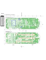
NOTE FOR PRINTED WIRING BOARDS AND SCHEMATIC DIAGRAMS
Note on Printed Wiring Board:
•
X
: parts extracted from the component side.
•
Y
: parts extracted from the conductor side.
•
z
: Through hole.
•
: Pattern from the side which enables seeing.
•
: Carbon pattern.
(The other layers' patterns are not indicated.)
Caution:
Pattern face side:
Parts on the pattern face side seen from
(Conductor Side)
the pattern face are indicated.
Parts face side:
Parts on the parts face side seen from
(Component Side)
the parts face are indicated.
Note on Schematic Diagram:
• All capacitors are in
µ
F unless otherwise noted. pF:
µµ
F
50 WV or less are not indicated except for electrolytics
and tantalums.
• All resistors are in
Ω
and
1
/
4
W or less unless otherwise
specified.
•
%
: indicates tolerance.
•
C
: panel designation.
•
A
: B+ Line.
• Power voltages are dc 9 V and fed with regulated dc power
supply from external power voltage jack (J3) on the BASE
MAIN board, dc 12 V and fed with regulated dc power
supply from modular jack (J1) on the BASE MAIN board
with 100
Ω
in series, and dc 3.6 V and fed with regulated
dc power supply from battery terminal (J5) on the HAND
MAIN board.
• Voltages and waveforms are dc with respect to ground in
test mode.
∗
: Impossible to measure
• Voltages are taken with a VOM (Input impedance 10 M
Ω
).
Voltage variations may be noted due to normal produc-
tion tolerances.
• Waveforms are taken with a oscilloscope.
Voltage variations may be noted due to normal produc-
tion tolerances.
• Circled numbers refer to waveforms.
• Signal path.
N
: RX
O
: TX
2.4Vp-p
30.5
µ
s
3.9 Vp-p
125 ns
3.9 Vp-p
125 ns
• Waveforms
– BASE MAIN Board –
1
U4
qh
(XOUT)
1 V/DIV, 50 ns/DIV
– HAND MAIN Board –
qa
U2
3
(XOUT)
1 V/DIV, 50 ns/DIV
qs
U2
7
(XTOUT)
1 V/DIV, 20
µ
s/DIV
1 Vp-p
279 ns
2
U3
5
(XOUT)
500 mV/DIV, 100 ns/DIV
• IC Block Diagram
– BASE MAIN Board –
U3
PCC318
Note: The components identified by mark
0
or dotted line
with mark
0
are critical for safety.
Replace only with part number specified.


