background image

– 31 –

– 32 –

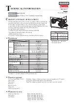
[BASE  MAIN  BOARD] (Component Side)

[BASE  MAIN  BOARD] (Conductor Side)

Adjustment Location:

FL101: RX level adjustment

L101: RX VT adjustment

L52: TX VT adjustment

RV101: RSSI (H) adjustment

TP201

TP202
AF ocillator: TX confirmation
Audio analyzer: RX level adjustment,

Confirmation of distortion factor,
Confirmation of RX gain

TP8 (RSSI)
TP14 (GND)
• oscilloscope: Adjustment of RSSI (H) gain,

Adjustment of RSSI (L) gain

TP1 (ANT)
TP3 (RF GND)
• Modulation analyzer: TX confirmation
• SG: RX adjustment

TP6 (TX VT)
TP15 (GND)
• digital voltmeter: TX VT adjustment

TP5 (RX VT)
TP14 (GND)
• digital voltmeter: RX VT adjustment

TP1

TP3

TP5

TP8

TP202

TP201

TP6

TP14

TP15

IC101

Summary of Contents for SPP-A400 - Cordless Telephone With Answering Machine

Page 1: ...ORDLESS TELEPHONE MICROFILM US Model Canadian Model SPECIFICATIONS SERVICE MANUAL SPP A700 For RM X2S Remote Commander please refer to RM X2S X3S Service Manual 9 960 039 previously issued Photo HCD D270 ...

Page 2: ...within 3 times Be careful not to apply force on the conductor when soldering or unsoldering Notes on chip component replacement Never reuse a disconnected chip component Notice that the minus side of a tantalum capacitor may be dam aged by heat SAFETY RELATED COMPONENT WARNING COMPONENTS IDENTIFIED BY MARK OR DOTTED LINE WITH MARK ON THE SCHEMATIC DIAGRAMS AND IN THE PARTS LIST ARE CRITICAL TO SAF...

Page 3: ... 3 This section is extracted from instruction manual SECTION 1 GENERAL ...

Page 4: ... 4 ...

Page 5: ... 5 ...

Page 6: ... 6 ...

Page 7: ... 7 ...

Page 8: ... 8 ...

Page 9: ... 9 ...

Page 10: ... 10 ...

Page 11: ... 11 ...

Page 12: ... 12 ...

Page 13: ... 13 ...

Page 14: ... 14 ...

Page 15: ... 15 ...

Page 16: ... 16 ...

Page 17: ... 17 ...

Page 18: ... 18 ...

Page 19: ... 19 ...

Page 20: ... 20 ...

Page 21: ...isassembly procedure in the numerical order given HAND SET REAR CABINET SECTION 2 DISASSEMBLY 2 two screws BTP 2 6 12 1 battery case lid 4 Removal the rear cabinet to direction of the arrow A 3 two claws 3 two claws claw A ...

Page 22: ...rew BTP 2 6 12 4 two screws BTP 2 6 8 5 HAND MAIN board 1 three screws BTP 2 6 8 2 three terminals charge H S 7 two connectors CN501 502 6 connector CN101 3 base set upper ass y 1 five screws P 3 10 2 two claws 2 two claws 4 three connectors CN301 501 502 ...

Page 23: ...h to the P PULSE side 2 Reset the POWER ON connect the AC adapter plug while pressing TIME REPEA T PLA Y ST OP keys 3 Set the DIAL MODE switch to the T TONE side After that back to the P PULSE side 4 Using the signal in step 3 as a trigger the base unit reads chan nel information with the key matrix and starts the Test mode 5 After the Test mode started the base unit generates a comple tion tone t...

Page 24: ...MUTING MUTING ON RX RF OFF RX AF OFF RX MUTING MUTING ON CID CW H AGC not present MEMO key 7 SEG LED all turn off and the condition of audio system in the base unit is kept as it is then a command is sent to the DSP and recording continues until MEMO key is pressed again Old mes sage is erased each time a new message is recorded where a garbage correction is made and new message is recorded at the...

Page 25: ...and the Test mode starts 3 Operationatstart up When the Test mode starts the Handset causes the ringer to sound for 500ms sets a channel depending on the key matrix condition so as to be ready for receiving Also the Handset sets the Liquid cristal display all turn on the RSSI gain to High and goes in the Test Mode Idle status For the COL0 COL3 logic of key matrix and channel setting refer to the f...

Page 26: ...REDIAL 1 2 3 4 5 6 7 8 9 0 If the keys are pressed in the above sequence the handset gener ates a key touch tone and when the input of all keys completed successfully it generates a completion tone and returns to the Test Mode Idle status In case of wrong key input sequence it gener ates an error tone and returns to the Test Mode Idle status 5 key RSSI gain is set to Low Once the gain is set to Lo...

Page 27: ...the demodulated waveform of modulation analyzer with a distortion meter to confirm that the distortion is below 3 0 Confirmation of the de gree of ID modula tion Press MEMO key to set the base unit in the Message Transmit Receive Test mode Measure the degree of modulation with a modulation analyzer to confirm that it is 2 0 3 5 kHz DEV Observe the demodulated waveform of modulation analyzer with a...

Page 28: ...BµV EMF then observe the RSSI signal with an oscilloscope to confirm that the RSSI gain is High SG TP1 ANT TP3 RF GND Frequency 48 760 MHz RF output 60 dB µV EMF Signal 1 kHz INT Deviation FM 3 kHz DEV SG TP1 ANT TP3 RF GND Frequency 48 760 MHz RF output 6 dB µV EMF Signal 1 kHz INT Deviation FM 3 kHz DEV AF oscillator TP1 ANT TP3 RF GND 20 Hz SG Frequency 48 760 MHz RF output 12 dB µV EMF Signal ...

Page 29: ...e demodulated waveform of modulation analyzer with a distortion meter to confirm that the distortion is below 2 0 Confirmation of the de gree of ID modula tion Press 6 key to set the Handset in the Message Transmit Re ceive Test mode Measure the degree of modulation with a modulation analyzer to confirm that it is 1 8 3 5 kHz DEV Observe the demodulated waveform of modulation analyzer with an osci...

Page 30: ...dBµV EMF then observe the RSSI signal with an oscilloscope to confirm that the RSSI gain is High SG ANTENNA TERMINAL TP3 RF GND Frequency 43 780 MHz RF output 60 dB µV EMF Signal 1 kHz INT Deviation FM 3 kHz DEV Audio analyzer MEAS mode Distortion Input range 10 dBV 3 Filter 400 Hz 20 kHz TP47 RX TP30 GND Audio analyzer MEAS mode Distortion Input range 10 dBV 3 Filter 400 Hz 20 kHz TP47 RX TP30 GN...

Page 31: ...firmation Audio analyzer RX level adjustment Confirmation of distortion factor Confirmation of RX gain TP8 RSSI TP14 GND oscilloscope Adjustment of RSSI H gain Adjustment of RSSI L gain TP1 ANT TP3 RF GND Modulation analyzer TX confirmation SG RX adjustment TP6 TX VT TP15 GND digital voltmeter TX VT adjustment TP5 RX VT TP14 GND digital voltmeter RX VT adjustment TP1 TP3 TP5 TP8 TP202 TP201 TP6 TP...

Page 32: ...D oscilloscope Adjustment of RSSI H gain Adjustment of RSSI L gain TP47 RX TP30 GND Audio analyzer RX level adjustment Confirmation of distortion factor Confirmation of RX gain TP6 TX VT TP30 GND digital voltmeter TX VT adjustment TP5 RX VT TP30 GND digital voltmeter RX VT adjustment ANTENNA TERMINAL TP3 RF GND Modulation analyzer TX confirmation SG RX adjustment ANT2 TP3 TP5 TP47 IC101 IC501 TP6 ...

Page 33: ......

Page 34: ......

Page 35: ......

Page 36: ......

Page 37: ......

Page 38: ......

Page 39: ... ADDR2 62 ADDR3 63 ADDR4 64 ADDR5 65 ADDR6 Not used 66 ADDR7 67 ADDR8 68 ADDR9 69 ADDR10 70 ADDR11 71 ADDR12 72 ADDR13 73 VCC Power supply 5 V 74 GND Ground 75 CE0 O Chip Enable 0 for Samsung Flash 76 CE1 Not used 77 CS I Chip Select Optional connection to ground recommended if not used 78 ALE O Address Latch Enable for Samsung Flash 79 CLE O Command Latch Enable for Samsung Flash 80 ADDR16 Not us...

Page 40: ... read write control H Read L Write 26 LCD RS O Liquid crystal display register select signal output 27 ROW5 O Row side of 4 6 key matrix 28 ROW6 O 29 Not used Open 30 31 MODEL SELECT I Model selection L SPP A400 32 TEST SW I For test mode start H Start 33 TEST ACT I Intermittent receive trigger in TEST mode H Start 34 BATT DET I Battery detection H BATT present 35 RSSI H L O RSSI gain selection L ...

Page 41: ... I Binary input Tone Pulse L T H P 21 MIC ON O Microphone ON OFF control L MIC ON 22 SP ON O Speaker ON OFF control L SP ON 23 ROW0 O Row side of 2 5 key matrix 24 ROW1 O 25 RX DATA I Receiving data input 26 WR O DSP WR 27 LED WR O 7 SEG driver write signal H Latch 28 RD O DSP RD 29 HI LO O DSP Hi Lo control 30 CHG LED O CHG LED control L LED ON 31 ANS LED O ANSWER LED L LED ON 32 DP O DP output H...

Page 42: ...n Remark Ref No Part No Description Remark 1 HAND SET SECTION rA HAND MICROPHONE board supplied with HAND MAIN board 1 X 3374 544 1 SET FRONT ASSY HAND 2 3 014 329 01 CUSHION SP 3 3 014 326 01 HOLDER SPEAKER 4 A 3672 339 A HAND MAIN BOARD COMPLETE 5 3 014 324 01 CABINET REAR 6 3 014 325 01 LID BATTERY CASE 7 3 014 327 01 TERMINAL CHARGE H S 8 A 3622 134 A HAND KEY BOARD COMPLETE 9 1 771 101 11 SWI...

Page 43: ...ied with BASE MAIN board Ref No Part No Description Remark Ref No Part No Description Remark 60 3 014 318 01 TERMINAL ANTENNA 61 3 014 314 01 CABINET LOWER 63 3 012 374 01 HOLDER HAND SET 64 3 831 441 XX CUSHION SPEAKER 65 3 007 173 01 LABEL TERMINAL CAUTION S 66 3 936 696 21 FOOT RUBBER ANT1 1 501 893 21 ANTENNA TELESCOPIC MIC501 8 814 186 00 MICROPHONE ELECTRET CONDENSER SP501 1 505 720 11 SPEAK...

Page 44: ...00 METAL CHIP 10K 5 1 10W R715 1 216 073 00 METAL CHIP 10K 5 1 10W R716 1 216 073 00 METAL CHIP 10K 5 1 10W R717 1 216 073 00 METAL CHIP 10K 5 1 10W R718 1 216 073 00 METAL CHIP 10K 5 1 10W SWITCH S701 1 572 381 21 SWITCH KEY BOARD PAGE S702 1 572 381 21 SWITCH KEY BOARD PLAY STOP S703 1 571 977 11 SWITCH TACTIL GREETING S704 1 571 977 11 SWITCH TACTIL ERASE S705 1 571 977 11 SWITCH TACTIL TIME S7...

Page 45: ...24 635 00 ELECT 220uF 20 6 3V C311 1 165 319 11 CERAMIC CHIP 0 1uF 50V C312 1 126 794 11 ELECT 4 7uF 20 50V C316 1 165 319 11 CERAMIC CHIP 0 1uF 50V C317 1 124 635 00 ELECT 220uF 20 6 3V C321 1 163 033 00 CERAMIC CHIP 0 022uF 50V C322 1 163 033 00 CERAMIC CHIP 0 022uF 50V C401 1 115 871 11 ELECT 1uF 20 50V C402 1 163 019 00 CERAMIC CHIP 0 0068uF 10 50V C403 1 164 700 11 CERAMIC CHIP 0 68uF 16V C40...

Page 46: ...HIP 3216 JR16 1 216 296 00 CONDUCTOR CHIP 3216 JR17 1 216 296 00 CONDUCTOR CHIP 3216 JR18 1 216 296 00 CONDUCTOR CHIP 3216 JR21 1 216 295 00 CONDUCTOR CHIP 2012 JR22 1 216 296 00 CONDUCTOR CHIP 3216 JR23 1 216 296 00 CONDUCTOR CHIP 3216 JR24 1 216 295 00 CONDUCTOR CHIP 2012 JR25 1 216 296 00 CONDUCTOR CHIP 3216 JR26 1 216 296 00 CONDUCTOR CHIP 2012 JR28 1 216 296 00 CONDUCTOR CHIP 3216 JR29 1 216 ...

Page 47: ...0W R201 1 215 864 00 METAL OXIDE 150 5 1W R202 1 216 073 00 METAL CHIP 10K 5 1 10W R203 1 216 105 00 METAL GLAZE 220K 5 1 10W R204 1 216 089 00 METAL GLAZE 47K 5 1 10W R205 1 216 113 00 METAL CHIP 470K 5 1 10W R206 1 216 097 00 METAL GLAZE 100K 5 1 10W R207 1 216 065 00 METAL CHIP 4 7K 5 1 10W R208 1 216 065 00 METAL CHIP 4 7K 5 1 10W R210 1 216 057 00 METAL CHIP 2 2K 5 1 10W R211 1 215 877 11 MET...

Page 48: ...ETAL GLAZE 1K 5 1 10W R662 1 216 049 11 METAL GLAZE 1K 5 1 10W R663 1 216 049 11 METAL GLAZE 1K 5 1 10W R664 1 216 049 11 METAL GLAZE 1K 5 1 10W R665 1 216 121 00 METAL GLAZE 1M 5 1 10W R666 1 216 049 11 METAL GLAZE 1K 5 1 10W R667 1 216 049 11 METAL GLAZE 1K 5 1 10W R668 1 216 198 00 METAL GLAZE 1K 5 1 8W R669 1 216 049 11 METAL GLAZE 1K 5 1 10W R670 1 216 049 11 METAL GLAZE 1K 5 1 10W R671 1 216...

Page 49: ... 296 00 CONDUCTOR CHIP 3216 A 3672 339 A HAND MAIN BOARD COMPLETE INCLUDING HAND MICROPHONE BOARD BAND PASS FILTER BPF1 1 239 918 11 FILTER BAND PASS BPF2 1 233 667 11 FILTER BAND PASS BPF51 1 239 916 11 FILTER BAND PASS CAPACITOR C2 1 163 031 11 CERAMIC CHIP 0 01uF 50V C3 1 163 037 11 CERAMIC CHIP 0 022uF 10 25V C4 1 164 232 11 CERAMIC CHIP 0 01uF 50V C5 1 163 083 00 CERAMIC CHIP 1PF 50V C51 1 16...

Page 50: ...8SB T1 D202 8 719 938 75 DIODE SB05 05CP D203 8 719 801 78 DIODE 1SS184 D301 8 719 801 78 DIODE 1SS184 D501 8 719 159 06 DIODE RD4 7SB T2 D502 8 719 801 78 DIODE 1SS184 D504 8 719 941 04 DIODE SB007 03CP FILTER FL101 1 409 671 11 COIL IFT FL101 1 416 311 11 COIL IFT IC IC101 8 759 462 29 IC TB31224F IC201 8 759 082 66 IC S 80727AL AQ T1 IC501 8 759 482 25 IC SH665316A 4J84 IC502 8 759 491 56 IC CA...

Page 51: ...100K 5 1 10W R204 1 216 097 00 METAL GLAZE 100K 5 1 10W R205 1 216 073 00 METAL CHIP 10K 5 1 10W R301 1 216 057 00 METAL CHIP 2 2K 5 1 10W R302 1 216 057 00 METAL CHIP 2 2K 5 1 10W R303 1 216 097 00 METAL GLAZE 100K 5 1 10W R304 1 216 097 00 METAL GLAZE 100K 5 1 10W R305 1 216 029 00 METAL CHIP 150 5 1 10W R306 1 216 073 00 METAL CHIP 10K 5 1 10W Ref No Part No Description Remark R503 1 216 202 00...

Page 52: ...SORIES PACKING MATERIALS 1 467 112 41 ADAPTOR AC AC T46 1 528 710 11 BATTERY NICKEL CADMIUM BP T16 1 543 584 31 CORE 1 696 454 11 CORD WITH MODULAR PLUG LINE 3 012 379 01 CASE WALL HOOK 3 016 498 11 GUIDE CARD QUICK START ENGLISH SPANISH US 3 016 498 21 GUIDE CARD QUICK START ENGLISH FRENCH Canadian 3 860 469 11 MANUAL INSTRUCTION ENGLISH SPANISH US 3 860 469 21 MANUAL INSTRUCTION ENGLISH FRENCH C...

Reviews: