background image

4-3.

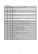
IC PIN FUNCTION

 IC1 (µPD753017)

µ

PD753017 is the 4-bit single-chip microprocessor for the LCD panel display with the built-in controller and driver.

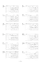
Pin No.

54

55

56

57

58

59

60

61

62

63

64

65

66

67

68

69 to 80

I/O

I

I

I/O

I/O

I/O

I/O

I/O

I/O

I/O

I/O

I

O

Pin Function

Positive power supply terminal.

Terminal to which sub-system clock oscillating crystal is connected.

When external clock is used, input the ext. clock to XT1 and leave XT2 open.

XT1 can be used as the 1-bit input (TEST) terminal.

Internally connected to VDD.

Terminal to which main system clock oscillating crystal/ceramic is connected.

When external clock is used, input the ext. clock to X1, and connect the inverted phase signal to XT2.

Parallel fall-down edge detection

testable input terminal.

Parallel fall-down edge detection

testable input terminal.

System reset input terminal.

Segment signal output terminals.

Pin Name

V

DD

XT1

XT2

VPP

X1

X2

P60/KR0

P61/KR1

P62/KR2

P63/KR3

P70/KR4

P71/KR5

P72/KR6

P73/KR7

RESET

S0 to S11

Programmable 4-bit input/output port. (PORT 8).

Input and output can be specified in units of bit.

The pull-up resistor built-in can be specified in units of

4 bits by software.

4-bit input/output port. (PORT 7).

The pull-up resistor built-in can be specified in units of

4 bits by software.

— 23 —

— 24 —

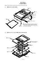
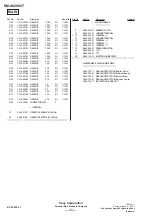
Pin No.

1 to 12

13 to 20

21 to 24

25

26 to 28

29 to 32

33

34 to 37

38

39

40

41

42

43

44

45

46

47

48

49

50

51

52

53

I/O

O

O

O

O

I/O

I/O

I

I/O

I/O

I/O

I

I

I

I

I/O

I/O

I/O

I/O

I/O

I/O

I/O

I/O

Pin Function

Segment signal output terminals.

1-bit output port (BIT-PORT). Used also as the segment signal output terminal.

Common signal output terminal.

Output terminal for cutting off the externally connected dividing resistor.

Power supply terminal for LCD drive. Dividing resistor are built-in. (mask option)

N-ch open-drain 4-bit input/output port. (PORT 4).

Pull-up resistor can be built-in in units of bit. (mask option).

10V withstand voltage in the open-drain connection.

GND terminal.

N-ch open-drain 4-bit input/output port. (PORT 5).

Pull-up resistor can be built-in in units of bit. (mask option).

10V withstand voltage in the open-drain connection.

Edge detection vector interrupt input terminal.

(Both of the rise-up and fall-down edge detections are usable.)

Serial clock input/output terminal.

Serial data output terminal.

Serial bus input/output terminal.

Serial data input terminal.

Serial bus input/output terminal.

Equipped with noise-rejection function.

Clock-synchronous type.

Asynchronous

Edge detection teatble input terminal.

(Rise-up edge detection). Asynchronous.

External event pulse input

terminal to the timer/event counter.

Timer/event counter output terminal.

Timer/event counter output terminal.

Clock output terminal.

Fixed frequency output terminal.

(For buzzer or for trimming the system clock.

Clock output terminal for driving the external expansion driver.

Clock output terminal for synchronizing the external expansion driver.

Pin Name

S12 to S23

BP0 to BP7/

S24 to S31

COM0 to COM3

BIAS

V

LC0

 to V

LC2

P40 to P43

Vss

P50 to P53

P00/INT4

P01/SCK

P02/SO/SB0

P03/S1/SB1

P10/INT0

P11/INT1

P12/INT2

P13/TIO

P20/PTO0

P21/PTO1

P22/PCL

P23/BUZ

P30/LCD CL

P31/SYNC

P32

P33

4-bit input port (PORT 0).

The pull-up resistor built-in can be

specified in units of 3 bits by

software for PO1 to PO3.

Edge detection vector interrupt

input terminal.(Detection edge

selectable.)

4-bit input port (PORT 1).

The pull-up resistor built-in can

be specified in units of 4 bits by

software.

4-bit input port (PORT 2).

The pull-up resistor built-in can be

specified in units of 4 bits by

software.

Programmable 4-bit input/output

port. (PORT 3).

Input and output can be set in units

of bit.

The pull-up resistor built-in can be

specified in units of 4 bits by

software.

Summary of Contents for RM-AV2000T

Page 1: ...ng on components of different manufacturers Power requirements Remote control Four R6 size AA batteries Backlight Two R6 size AA batteries Battery life Apporox 6 months varies depending on frequency of use Dimensions Approx 120 175 45 mm 43 4 7 113 16 in w h d Mass 290g 10 22 oz not including batteries Design and specifications are subject to change without notice ...

Page 2: ...ESE COMPONENTS WITH SONY PARTS WHOSE PART NUMBERS APPEAR AS SHOWN IN THIS MANUAL OR IN SUPPLEMENTS PUBLISHED BY SONY 1 GENERAL 3 2 DISASSEMBLY 2 1 Removal of case lower 15 2 2 Removal of T T P LCD rubber switch main bard 15 3 TEST MODE 16 4 DIAGRAMS 4 1 Printed Wiring Board Main Section 19 4 2 Schematic Diagram Main Section 21 4 3 IC Pin Functions 23 5 EXPLODED VIEWS 26 6 ELECTRICAL PARTS LIST 27 ...

Page 3: ... 3 SECTION 1 GENERAL This section is extracted from instruction manual ...

Page 4: ... 4 ...

Page 5: ... 5 ...

Page 6: ... 6 ...

Page 7: ... 7 ...

Page 8: ... 8 ...

Page 9: ... 9 ...

Page 10: ... 10 ...

Page 11: ... 11 ...

Page 12: ... 12 ...

Page 13: ... 13 ...

Page 14: ... 14 ...

Page 15: ...crewdriver tip in between the Case upper and the Case lower When the Cases are opened a little insert nail of your thumb into the clearance Open the Covers while sliding the Covers upwards Case upper 2 K2 8 Case lower Case upper Claw 6 Precision screwdriver 2 K2 8 1 Battery lid 4 2 Case upper 3 Remove soldering of the T T P and remove it 4 LCD Case lower 1 P2 5 6 MAIN board 5 Rubber switch ...

Page 16: ...is normal 4 Press all keys of the Operation panel key block except the COMMANDER OFF key and of the LCD touch key block sequentially When all keys are pressed confirm that the long buzzar sound and all LCD displays are turned off NOTE Be careful that all data in S RAM is cleared when the above TEST mode is performed This TEST Mode can be terminated in its middle before testing all keys by pressing...

Page 17: ...y DC 6V constant voltage 2 Take reading of frequency counter indication value This value is named fA 3 Turn off the regulated power supply then turn OFF the switch SW1 After that turn back ON the regulated power supply 4 Take reading of frequency counter value in the same way as step 2 This value is named fB 5 Using the frequency values that are measured in steps 2 and 4 calculate the crystal osci...

Page 18: ...ed b Switch pattern 19 20 Ref No Location Semiconductor Location Ref No Location D1 B 10 D2 B 9 D3 B 8 D4 B 7 D5 E 10 D6 A 9 D10 E 10 D11 E 10 IC1 B 9 IC2 D 8 IC3 E 9 IC4 B 10 IC5 E 10 IC6 B 8 IC7 C 9 IC8 E 8 Q1 B 9 Q2 B 7 Q4 E 10 Q9 D 9 Q10 D 10 Q11 E 10 Q12 D 9 Q13 D 9 Q14 F 9 Q15 F 9 Caution Pattern face side Parts on the pattern face side seen from Conductor Side the pattern face are indicated...

Page 19: ... VDD GND IP54 IP53 IP56 IP55 RDO REC AD7 AD8 AD5 AD6 ADA OUTP AD9 ADB AD3 AD4 GND AD2 AD0 AD1 OD6 OD7 OD4 OD5 OD2 OD3 OD0 OD1 WTO OCE S10 S11 S8 S9 S6 S7 S4 S5 S2 S3 S0 S1 P73 RESET P71 P72 P63 P70 P61 P62 IRDN IWIN IENN X1 4 0MHz X2 32 768kHz C13 33p C14 33p P73 P72 P71 P70 P63 P62 P61 P60 P20 P22 P21 R22 27 R21 330k R57 1k BZ1 BUZZER DRIVE Q9 MSD601 R56 4 7K R50 4 7K R51 10k R52 470 R53 4 7k R54...

Page 20: ...or are built in mask option N ch open drain 4 bit input output port PORT 4 Pull up resistor can be built in in units of bit mask option 10V withstand voltage in the open drain connection GND terminal N ch open drain 4 bit input output port PORT 5 Pull up resistor can be built in in units of bit mask option 10V withstand voltage in the open drain connection Edge detection vector interrupt input ter...

Page 21: ... which external memory is connected Lower address AD2 to AD7 Terminals to which external memory is connected Upper address AD8 to AD11 Not used Remote control signal output Remote control signal receiver block ON OFF output SRAM IC3 W24257S ADD and IC8 LH5359PA ADD SRAM IC3 W24257S ADE and IC8 LH5359PA ADE Selector SRAM IC3 W242575S or ROM IC8 LH5359PA EL control output Dark GND terminal Positive ...

Page 22: ... 685 205 19 SCREW KTP2 8 TYPE2 NON SLIT 2 9 880 055 01 HOLDER 3 9 880 050 01 LID BATTERY CASE 4 7 685 103 19 SCREW P2 5 TYPE2 NON SLIT 5 9 995 523 01 FOOT RUBBER 6 9 880 048 01 RUBBER SWITCH 7 9 880 049 01 CASE LOWER 8 9 880 057 01 SPACER 9 9 995 525 01 LCD BRACKET 10 9 880 051 01 SEAL 11 9 995 518 01 SMOKE PLATE 12 9 880 458 01 CASE UPPER 13 9 995 521 01 COMMON TERMINAL 14 9 995 529 01 TERMINAL 1...

Page 23: ...TOR 14P CN2 9 880 018 01 CONNECTOR 4P DIODE D1 9 880 014 01 DIODE UR64LD1 D2 9 880 014 01 DIODE UR64LD1 D3 9 880 014 01 DIODE UR64LD1 D4 9 880 014 01 DIODE UR64LD1 D5 8 719 938 72 DIODE SB01 05CP D6 9 880 013 01 DIODE TPS705WMATU2 D10 8 719 421 51 DIODE MA738 TX D11 8 719 421 51 DIODE MA738 TX IC IC1 9 880 457 01 IC uPD753017E11 IC2 9 995 541 01 IC uPD65012F251 IC3 9 880 455 01 IC W24257S70LL IC4 ...

Page 24: ...91 RES CHIP 1K 5 1 10W R60 1 216 053 00 RES CHIP 1 5K 5 1 10W R61 1 216 022 91 RES CHIP 82 5 1 10W R70 1 213 073 91 RES CHIP 10K 5 1 10W R71 1 216 077 00 RES CHIP 15K 5 1 10W R72 1 216 089 91 RES CHIP 47K 5 1 10W R84 1 216 295 91 CONDUCTOR CHIP 0 VIBRATOR X1 9 880 017 01 VIBRATOR CERAMIC 4 00MHz X2 9 880 015 01 VIBRATOR CRYSTAL 32 768kHz MISCELLANEOUS 6 9 880 048 01 RUBBER SWITCH 13 9 995 521 01 C...

Reviews: