background image

18

RCD-W500C

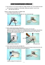
3-23. Gear (Chucking)

Precaution During Gear (Gear U/D Slider),  Gear (Gear B), Gear (Gear A) Installation

1

Slide the slider (U/D)
fully in the arrow 
direction.

slider (U/D)

3

gear (gear B)

2

gear (U/D slider)

4

gear (gear A)

portion A

Adjust the gear (gear B) with the 
portion A as shown.

slider (U/D) gear

Adjust the gear so that it meshes with
the bottom tooth of slider (U/D) gear,
as shown.

gear
(gear B)

linearly

Adjust so as to be aligned with
gear B linearly, as shown.

PRECAUTION DURING 
GEAR (CHUCKING) (2)

PRECAUTION DURING 
GEAR (CHUCKING) (1)

OK

NG

3

gear (chucking)

rotary encoder (S707)

1

2

gear 
(chucking)

rotary encoder (S707)

rotary encoder
(S707)

Align with the slot of
rotary encoder.

Align marking.

Summary of Contents for RCDW500C - Compact Disc Player

Page 1: ...m Laser Semiconductor laser 780 nm Emission duration continuous Playable discs CD CD R CD RW Recordable discs CD R CD RW for Audio Frequency response 20 Hz 20 000 Hz 0 5 dB Signal to Noise Ratio Over 98 dB during play Wow and flutter Below measurable limit Inputs ANALOG IN Impedance 47 kilohms Phono jacks Rated input 500 mVrms Minimum input 250 mVrms DIGITAL OPTICAL IN Square optical connector jac...

Page 2: ...S NUMÉROS SONT DONNÉS DANS CE MANUEL OU DANS LES SUPPÉMENTS PUBLIÉS PAR SONY After correcting the original service problem perform the following safety checks before releasing the set to the customer Check the antenna terminals metal trim metallized knobs screws and all other exposed metal parts for AC leakage Check leakage as described below LEAKAGE The AC leakage from any exposed metal part to e...

Page 3: ...s CD R Section 4 4 68 6 12 Printed Wiring Boards MAIN Section Side A 69 6 13 Printed Wiring Boards MAIN Section Side B 70 6 14 Schematic Diagrams MAIN Section 1 2 71 6 15 Schematic Diagrams MAIN Section 2 2 72 6 16 Printed Wiring Boards LED Section 73 6 17 Schematic Diagrams LED Section 74 6 18 Printed Wiring Boards DISPLAY Section 75 6 19 Schematic Diagrams DISPLAY Section 76 6 20 IC Block Diagra...

Page 4: ...back in DECK A or with an external device such as CD ROM or VIDEO CD Remove the disc and then insert a music CD for playback Recording has not been completed successfully because of vibration Relocate the unit in a place free of vibration and restart the recording again The disc you try to record is excessively dirty such as oil stained or finger marked or scratched Or the disc is not normal Repla...

Page 5: ...button q ERASE button qa SBM button and indicator qs REC z button qd X button qf REC LEVEL knob qg x button qh PLAY MODE button qj TIME button qk DISPLAY button ql YES button w l AMS L knob wa CLEAR button ws MENU NO button wd l AMS L knob wf ALBUM button wg PLAY MODE button wh TIME button wj x button wk PHONES jack wl X button e PHONE LEVEL knob 2 5 9 78 q qa qs qd qf qg qh qj qk ql w wd wa wf wj...

Page 6: ...CAA CAM CH LOADING PANEL CDR CD MECHANISM DECK CDM53L 30B61M CD MECHANISM DECK CDM65 RBD2 FITTING BASE MAGNET ASSY FITTING BASE GUIDE ASSY BRACKET CHASSIS LOAD MOTOR BOARD MOTOR LOADING ASSY STOCKER SECTION GEAR GEAR A GEAR GEAR B GEAR U D SLIDER GEAR CHUCKING SLIDER SELECTION TENSION SPRING SHUTTER SLIDER SHUTTER TRAY SUB CHASSIS MOLD B BD BOARD OPTICAL BLOCK SECTION CLAMP MOTOR BOARD MOTOR CLAMP...

Page 7: ... 3 1 Case 409538 3 2 Loading Panel CDR 4 case 409538 2 two screws case 3 TP2 3 8 3 two screws case 3 TP2 3 8 1 two screws case 3 TP2 3 8 1 Slide the lever cam CH to the direction of arrow Front panel side CD mechanism deck CDM65 RBD2 3 2 lever cam CH two hooks 4 loading panel CDR ...

Page 8: ...2pin CN900 2 connector 3pin CN690 4 connector 2pin CN920 5 three screws BVTP 3 8 6 four screws BVTP 3 8 3 wire flat type 21core CN671 5 three screws BVTP 2 6 8 7 four claws 2 two knobs AMS 1 knob AMS 6 twelve screws BVTP 2 6 8 3 four screws BVTP 2 6 8 4 SW board 8 LED board q DISP board 9 wire flat type 21core CN700 ...

Page 9: ...R mechanism deck CDM65 RBD2 1 Slide the lever cam CH to the direction of arrow 4 tray 2 Pull the tray while pressing the claw of the chassis in the direction of the arrow 3 Pull the tray while pressing the claw of the chassis and the claw of the tray in the direction of the arrow front panel side lever cam CH claw claw chassis chassis ...

Page 10: ...lexible flat cable 32core CN101 4 flexible flat cable 11core CN102 5 flexible flat cable 11core CN103 9 CDR board 2 bottom plate 1 four screws BVTP 2 6 8 1 Slide the cam CH to the direction of arrow 2 Remove the belt loading from the pulley of the motor assy 3 two claws 4 motor assy loading M201 ...

Page 11: ...b assy 1 two claws 2 two claws 5 dust cover 8 flexible flat cable 32core from optical device 1 flexible flat cable 11core CN103 2 flexible flat cable 11core CN102 3 flexible flat cable 32core CN101 4 two step screws 5 two screws 2X9 G with p tappin 9 optical pick up KRM 220CAA 6 two insulators main 7 two insulators main ...

Page 12: ...ear B q screw BVTP 3 8 6 wire flat type 25core CN660 8 wire flat type 17core CN640 7 wire flat type 9core CN661 1 wire flat type 21core CN671 4 connector 4pin CN111 5 connector 2pin CN900 2 connector 3pin CN690 9 connector 5pin CN641 3 wire flat type 11core CN630 qs three screws BVTP 3 8 qa bracket TR qj MAIN board qh power transformer qd four screws BVTT 3 6 qf two screws BVTT 3 6 qg Remove the s...

Page 13: ...ng Base Magnet Assy 2 four screws BVTP 3 8 5 wire flat type 17core CN701 4 wire flat type 9core CN105 3 wire flat type 25core CN102 1 connector 5pin CN713 6 CD mechanism deck CDM53L 30B61M 1 connector 3pin CN710 3 fitting base magnet assy 2 four screws BTTP M2 6 ...

Page 14: ...uide Assy Bracket Chassis 2 two screws BTTP M2 6 1 belt mode 3 Remove the two solderings 5 motor clamp assy M701 4 CLAMP MOTOR board 1 two connectors CN709 715 6 bracket chassis 3 fitting base guide assy 2 four screws BVTP 2 6 8 4 two screws BVTP 2 6 8 5 three screws BVTP 2 6 8 ...

Page 15: ...removed 3 Rotating the pulley LD shift the slider selection in the arrow B direction 4 Rotating the pulley mode in the arrow direction remove the tray sub to be removed 1 three screws BTTP M2 6 2 Insert the gear eject under the gear LD deceleration 1 Insert the portion A of chassis mold B into the portion B of slider selection gear eject portion A portion B of slider selection 3 gear eject 2 chass...

Page 16: ...M702 6 LOAD MOTOR board 1 belt communication 3 belt loading1 2 belt loading1 5 Remove the two solderings 4 stocker section 2 two step screws gear gear A 3 two step screws Hook the portion A of tray SUB to the slider selection portion A of tray SUB sticking of slider selection PRECAUTION DURING STOCKER SECTION INSTALLATION 1 ...

Page 17: ...TALLATION 2 1 two floating screws PTPWHM 2 6 x 6 2 washer 3 compression spring gear 4 slider selection tension spring shutter slider shutter slider selection gear chuking Insert a convex portion into the groove of gear chucking Insert the slider selection into the portion A portion A 7 screw BTTP M2 6 6 gear gear B 8 gear U D slider 5 gear gear A 2 washer 3 compression spring 4 gear selection 1 ge...

Page 18: ... gear gear B with the portion A as shown slider U D gear Adjust the gear so that it meshes with the bottom tooth of slider U D gear as shown gear gear B linearly Adjust so as to be aligned with gear B linearly as shown PRECAUTION DURING GEAR CHUCKING 2 PRECAUTION DURING GEAR CHUCKING 1 OK NG 3 gear chucking rotary encoder S707 1 2 gear chucking rotary encoder S707 rotary encoder S707 Align with th...

Page 19: ...he four points 1 flexible flat cable 16core CN101 3 hook 3 25 Optical Block Section 1 two floating screws PTPWHM 2 6 3 shaft BU holder 4 optical block section gear chucking gear chucking 2 Rotate the pulley LD in the direction of 2 to move the shaft BU holder upper ...

Page 20: ... Press the POWER button to POWER off BU Test Mode Deck A Procedure 1 Enter the test mode then turn the l AMS L DECK B knob to display BU Test and press the l AMS L DECK B knob 2 bdt S CURVE is displayed This test mode is used in the Elec trical Adjustment section 3 Turn the l AMS L DECK B knob bdt RAM READ bdt RAMWRITE bdt COMOUT bdt FB TUNE and bdt ERR RATE are displayed 4 To exit from this mode ...

Page 21: ...g the button 5 Press the POWER button to POWER off Remote Commander Check Procedure 1 Enter the test mode then turn the l AMS L DECK B knob to display RM CHECK and press the l AMS L DECK B knob 2 Press the H key on the remote commander then Got PlayCom is displayed 3 Press the MENU NO button then RM CHECK is displayed again 4 To exit from this mode turn the l AMS L DECK B knob to display Ship Mode...

Page 22: ...operation of finalize 13 PMA erasing 14 emergency 15 recording preparation 16 recording end examples 4 Start time of read in compression method bit 15 to bit 13 min 0 97 min 1 96 min 2 95 min 7 others bit 12 to bit 7 sec bit 6 to bit 0 frame examples 0000 1101 1000 0000 0001 0001 0001 0110 0D 80 11 16 7 0 frame 6 5 4 3 2 1 34 sec 97 min 22 frame 0 15 14 13 12 11 10 9 8 Start time of read in 97 27 ...

Page 23: ... RF signal level is correct or not CD SECTION DECK A Note A clear RF signal waveform means that the shape can be clearly distinguished at the center of the waveform Checking Location BD board Side B See page 24 E F Balance Adjustment Connection Procedure 1 Connect an oscilloscope to TP2 TE and TP7 VC on the BD board 2 Turn the power on 3 Load the disc YEDS 18 and playback the number five track 4 E...

Page 24: ...24 RCD W500C Adjustment and Checking Location BD BOARD SIDE B IC101 TP7 VC IC103 IC102 RV101 E F Balance Adjustment TP8 RFAC TP4 FE TP2 TE ...

Page 25: ...g of Programs 1 1 Connection Jig CONTROL FIRM RESET 0 756 358 11 CDM65 RBD1 SERVICE To RCD W500C CDM65 RBD2 Jig A B C D B C D Test Disc COM1 PC w SerialI F Laser Power Cables for Jig connecting Meter Oscilloscope MPXOUT RS 232C Cable 3 5 7 1 6 8 9 2 CDM65 RBD2 jig 4 Fig Position of Jig Set the jig after removing the cover of CDM65 RBD2 ...

Page 26: ...001 Parts No J 2501 046 A 7 Test Disc PATD 012 Parts No 4 225 203 1 Adjustment for Playback CD CD R TCD W091W Parts No J 2501 226 A Adjustment for Playback CD RW CRM74 Blank CD R Adjustment and Check for Recording CD R CWM74 Blank CD RW Check for Recording CD RW TCD W032W Parts No J 2501 227 A Defocus tolerance CD RW 8 RS 232C Cable 9 Cables for Jig connecting PH 5p PH 4p FFC 11p 1 0mm pitch J 250...

Page 27: ...the serial port from OS a Select Start Settings Control Panel and select System Device manager Communication Port COMn see Fig 1 1 Specify the COM port that connected with JIG of CDM65 b Double click COMn as you connect to the Jig CDM65 Set the parameters as below Bits per second 38400 Data bits 8 Parity non Stop bits 1 Flow control hardware see Fig 1 2 4 Fig 1 1 4 Fig 1 2 ...

Page 28: ...tl file and FUNC folder which are contained in 030416_Service and paste them in the Ttermpro file as below The file 030416_Service zip is distributed together with the service manual Note Do not change the directory path 5 Start up the TeraTermPro Double click the ttermpro exe 6 Set up the TeraTermPro IMPORTANT a Select Setup Serial Port and set the parameters as below Port As you connect to the J...

Page 29: ...tup Select Setup Save setup and save as teraterm ini in the Ttermpro directory see Fig 1 8 4 Fig 1 6 4 Fig 1 7 4 Fig 1 8 4 Fig 1 9 7 Connect the JIG and CDM65 8 Confirm the S510 on JIG is CONTROL 9 Power on the CDM65 and press SW101 RESET on JIG CDM65 RBD1 has connected with this PC is displayed see Fig 1 9 If above message is not displayed you may have some mistakes Please confirm previous settin...

Page 30: ...ir works as shown below electrical adjustment is required KRM 220CAA is replaced RBD2 is replaced The parts shown in the List 1 is replaced Locating the faulty point Electrical adjustment Electrical adjustment is not required List 1 IC101 IC103 IC171 IC201 IC502 Yes Yes Yes No No No ...

Page 31: ... Place probe of a laser power meter in the specified position following the display as shown in Fig 3 3 See Fig 3 3 a jig CDM65 RBD2 optical pick up sensor probe 4 Fig 3 3 a 3 Locating the Faulty Point 3 1 Laser Power Check 2 Press the RESET button SW101 of the jig as prompted by the display Note Do not add stress to an optical pick up ...

Page 32: ...e display shown in Fig 3 6 appears set the Range of a laser power meter to 10 mW and press OK 7 Check that the laser power meter reading satisfies the following requirement When the laser power satisfies the required specification press OK Fig 3 7 LEADER LPM 8001 4 5 to 4 7 mW 8 Check that the laser power meter reading satisfies the following requirement When the laser power satisfies the required...

Page 33: ...terioration Judgment 1 Select the menu as follows Control Macro and select 10vwdcC_S ttl Press Open Fig 3 10 3 11 4 Fig 3 9 4 Fig 3 10 4 Fig 3 11 2 Press the RESET button SW101 of the jig as prompted by the display 3 When the message OK appears as shown in Fig 3 12 press the OK button When the laser unit KRM 220CAA Op is normal without deterioration of laser the message OK appears If the laser uni...

Page 34: ...lowing the Connection Diagram as shown in section 1 1 2 Turn on the power of the RCD W500C in which the CDM65 is installed 3 Start up the TeraTermPro that is installed in PC Set the switch S510 on the jig to CONTROL 4 Press the RESET button SW101 of the jig Fig 3 14 5 Type portchk Enter from keyboard of PC Fig 3 15 Note 5 1 When the KRM 220CAA is connected the spindle motor rotates at a high speed...

Page 35: ...n Fig 3 16 is defective or its peripheral has abnormality Perform the repair work again and repeat the self diagnosis Repeat the repair work and self diagnosis until OK is displayed 4 Fig 3 16 7 Perform the operation check 3 4 Use of Self Diagnosis Function 2 In the case when result data of the past electrical adjustment should be left saved Perform the self diagnosis as described below in the cas...

Page 36: ...ked up Fig 3 20 4 Fig 3 19 4 Fig 3 20 4 Perform step 1 through step 6 of section 3 3 Use of Self Diagnosis Function 1 5 Select the menu as follows Control Macro and select E2recvF ttl Press Open 6 Press the RESET button SW101 of the jig as prompted by the display Fig 3 21 7 Type the filename in which result of electrical adjustment is saved Press OK Fig 3 22 4 Fig 3 21 4 Fig 3 22 ...

Page 37: ...sition of Elapsed Operating Hours Check if error has occurred or not by performing the following steps If error has occurred it is interpreted and saved in the specific directory Check contents of the error by viewing the specific directory as described below 1 Select the menu as follows Control Macro and select ErrHistGetAll_S ttl Press Open Fig 3 24 3 25 4 Fig 3 24 4 Fig 3 25 ...

Page 38: ...ory 5 The elapsed operating hours is shown at the top of EEPROM_Errorlog txt regardless of presence absence of the error history Check the elapsed operating hours from the display as shown in Fig 3 28 4 Fig 3 26 4 Fig 3 27 4 Fig 3 28 Error log example SN xxxx Op elapsed time 12 0 56 Spindle elapsed time 17 9 44 Error Log data 0 Error Pointer 38 Error Code 05 04 E0 00 00 01 0D 0D Focus is dropped 1...

Page 39: ...SW101 of the jig as prompted by the display 4 Press the RESET button SW101 of the jig again as prompted by the display 5 When the display as shown in Fig 4 2 appears type the serial number see Fig 4 3 that is printed on the label attached to the RBD2 This dialog appears only when the EEPROM IC502 is replaced When the display as shown in Fig 4 4 appears press No When the display as shown in Fig 4 5...

Page 40: ...w LEADER LPM 8001 0 81 0 05 mW 0 76 to 0 86 mW To increase the laser output power Press Yes of the Up dialog box To decrease the laser output power Press No of the Up dialog box and then press Yes of the Down dialog box Repeat until the laser output power satisfies the specification Fig 4 8 4 9 When the setting value is determined Press No of the Up dialog box and then press No of the Down dialog ...

Page 41: ...ss No of the Down dialog box and press Yes of the Save dialog box Fig 4 14 11 Adjust the laser output power as follows The laser output power i e laser power meter reading should satisfy the specification shown below LEADER LPM 8001 9 4 0 2 mW 9 2 to 9 6 mW To increase the laser output power Press Yes of the Up dialog box To decrease the laser output power Press No of the Up dialog box and then pr...

Page 42: ...1 peripheral and the sled drive mechanism 4 1 2 Power CAL NG Contents This message appears when the laser emission intensity is outside the specification Measure Check peripheral of CN101 Replace KRM 220CAA 4 2 CD CD R Playback Adjustment 1 Select the menu as follows Control Macro and select 02cdr_S ttl Press Open 2 Place the test CD disc PATD 012 on the tray as prompted by the display and press O...

Page 43: ... of the waveform RF signal waveform VOLT DIV suitable value TIME DIV 500ns 4 Fig 4 22 RF signal waveform VOLT DIV suitable value TIME DIV 500ns 4 Fig 4 23 RF signal waveform VOLT DIV suitable value TIME DIV 500ns 4 Fig 4 25 4 Fig 4 24 4 Fig 4 26 7 Check that the message CDR PB CAL completed appears The tray opens NG Judgment Result Indication 4 2 1 Playback Measurement NG Contents This message app...

Page 44: ...29 check that the waveform as shown in Fig 4 28 appears on an oscilloscope 5 As prompted by the message shown in Fig 4 31 check that the waveform as shown in Fig 4 30 appears on an oscilloscope 6 As prompted by the message shown in Fig 4 33 check that the waveform as shown in Fig 4 32 appears on an oscilloscope 4 Fig 4 29 RF signal waveform VOLT DIV suitable value TIME DIV 500ns 4 Fig 4 28 4 Fig 4...

Page 45: ...y Sony The disc that is used by this step cannot be used for the general purposes and for the purpose of operation check of the RCD series equipment The disc that is used for the general purposes or for the purpose of operation check of the RCD series equipment cannot be used in this step If the recording is interrupted by any reasons during the recording operation i e the WRITE POWER ON LED of th...

Page 46: ...in Fig 4 42 check that the waveform as shown in Fig 4 41 appears on an oscilloscope 4 Fig 4 37 4 Fig 4 38 4 Fig 4 40 4 Fig 4 42 RF signal waveform VOLT DIV suitable value TIME DIV 500ns 4 Fig 4 39 RF signal waveform VOLT DIV suitable value TIME DIV 500ns 4 Fig 4 41 8 Check that the message CDR REC CHECK completed appears The tray opens Stop playback 4X and exit from the test mode Deck A refer to p...

Page 47: ...c If the recording is interrupted by any reasons during the recording operation i e the WRITE POWER ON LED of the jig is lighting the disc cannot be used any more in the subsequent step In such a case erase the CD RW disc and repeat this step from the very beginning again 3 When the disc that is used in step 2 is the disc that has been used in the electrical adjustment in the past Press Yes When t...

Page 48: ...rs on an oscilloscope 8 Check that the message CDRW REC CHECK completed appears Fig 4 50 The tray opens Stop playback 4X and exit from the test mode Deck A refor to page 21 NG Judgment Result Indication 4 5 1 CD RW Playback Measurement NG Contents This message appears when the BLER Block Error Rate Beta m11 of the track that is recorded and played back is outside the specification Measure Check if...

Page 49: ...ge appears when writing data into EEPROM fails Measure When the steps of 01ldp_S ttl through 05cdrw_S ttl have no problem and the error occurs only in this step it is assumed that an error has occurred momentarily in the interface between PC and CDM65 Therefore repeat execution of 06vwdc_S ttl again 4 6 2 VWDC judge Line Top End NG Contents This message appears when the VWDC value is outside the s...

Page 50: ...justment has not completed within the specified time RPINWADJ2 NG The Read Power during Write2 Adjustment has not completed within the specified time SERVOSET NG The Servo Setting has not completed within the specified time TSa NG The ATIME Search has not completed within the specified time PLAYSW NG The Play operation has not started within the specified time STOP NG The Stop operation has not co...

Page 51: ...r History 1 Select the menu as follows Control Macro and select ErrHistClear ttl Press Open Fig 5 1 5 2 4 Fig 5 1 4 Fig 5 2 2 Press the RESET button SW101 of the jig as prompted by the display 3 Check that the message completed appears Fig 5 3 4 Fig 5 3 ...

Page 52: ... and install the TCD W032W in Deck B 2 Rotate the l AMS L Deck B knob to select the track 16 Start playback by pressing the same knob or by pressing the H Deck B button 3 Perform playback for 10 seconds or more and confirm that there is no abnormality such as sound skipping and others ...

Page 53: ...justment or to use a disc other than blank Be sure to erase it in the following procedure to use the disc used for electrical adjustment for other uses 4 Fig A 1 4 Fig A 2 4 Fig A 3 1 Select the menu as follows Control Macro and select RWeraseA ttl Press Open Fig A 1 A 2 2 Press the RESET button SW101 of the jig as prompted by the display Fig A 3 ...

Page 54: ...own by the arrow mark in Fig A 4 is updated after a while 4 Fig A 4 4 When update of time display is stopped and rotation of spindle is stopped press the STOP button SW501 of the Jig and then press the EJECT button SW508 of the jig to remove the disc ...

Page 55: ... Indication of transistor THIS NOTE IS COMMON FOR PRINTED WIRING BOARDS AND SCHEMATIC DIAGRAMS In addition to this necessary note is printed in each block Note The components identified by mark 0 or dotted line with mark 0 are critical for safety Replace only with part number specified Note Les composants identifiés par une marque 0 sont critiques pour la sécurité Ne les remplacer que par une pièc...

Page 56: ...1 2 4 1 2 4 IC504 5V D SDATAI HOST 15 1 2 4 IC506 XREQI 7 IC505 1 2 4 10 8 14 12 5 3 IC503 SDATAO HOST 13 XRDYO 8 5V D XREST 63 XMMUTE 96 TMP 84 SLFG 93 A SDATAI HOST SDATAO HOST XREQ RESET REV 99 FWD 100 XRDY DIN1 13 12 IC301 1 6 11 10 IC301 2 6 DIN2 1 2 IC301 3 6 3 4 IC301 4 6 1 2 4 IC302 5V D DOUT IC103 4 4 IC104 2 3 2 6 IC104 1 3 1 7 IC104 3 3 9 8 IC301 5 6 2 4 IC150 GATE 21 MIRR XRC 2 95 SPFG...

Page 57: ...11 76 ADA_RST PDOWN 5 75 ADA_INT0 INT0 6 74 ADA_INT1 INT1 7 TX3 16 RX4 4 DIGITAL IN OPTICAL IC610 DIGITAL OUT OPTICAL IC620 14 TX2 2 RX3 44 RX2 38 L IN 32 L OUT DIN2 DIN1 DOUT SDATAO HOST SDATAI HOST XREQ XRDY RESET J310 L R L R J790 PHONES Q380 MUTE SWITCH MUTE Q181 MUTE Q191 MUTE Q281 MUTE Q291 IC310 1 2 IC310 2 2 IC370 2 2 IC370 1 2 IC390 2 2 IC390 1 2 37 R IN 33 R OUT 85 A_MUTE 66 A_IN_SW SCMS...

Page 58: ...POWER DOWN IC476 D431 434 TR900 S921 POWER AC IN RESET IC480 2 1 AC AC TO CD R LINE FILTER LF900 36V REG IC460 1 3 36V D461 7V REG IC440 1 3 D451 454 8V REG IC430 1 3 CD 8V CD 7V 8V REG IC450 1 3 M 8V 5V REG IC420 1 3 3 3V REG IC426 1 3 D 5V D412 A 5V DVDD 5V D472 D471 D401 404 B B D473 SYS 3 3V RFVDD 3 3V CODEC 3 3V 5V REG IC410 1 3 D 5V D411 D422 D421 D407 D406 12 S RST 13 XOUT 15 XIN CD SYSTEM ...

Page 59: ... 2 IC122 C 5 Q101 C 3 Semiconductor Location IC104 IC101 IC122 IC102 IC103 IC105 E TP7 VC TP4 FE TP2 TE TP8 RFAC TP6 RFDC 69 69 660 A MAX 4T C248 C228 C301 C164 C163 C303 C302 R302 R320 FB101 R301 1 8 9 16 R228 FB202 C307 R315 9 1 5 4 2 3 1 JR2 R208 C304 C305 R304 R165 C157 C160 C159 CN103 CN105 R158 R157 R161 C158 25 R305 R229 1 20 21 40 41 60 61 80 1 2 A B C D 3 4 5 6 7 B A ...

Page 60: ...R233 R231 R232 C156 R208 R302 R126 R125 R117 R113 FB202 IC122 C260 R309 Q101 IC103 IC104 R308 C304 FB203 C305 C211 R206 C226 R114 C118 C119 C258 C254 R249 C228 C253 C121 CN103 IC101 IC105 IC102 R312 C222 R219 C103 C101 C102 R229 FB161 C248 C224 47k 33k 0 1 16P 68k 10k 150k 47 4V 0 1 0 1 0 1 3 3 0 068 0 1 B 0 022 100k 2 2k 100 10V 33k 1k 33p 0 1 B 100 10V 330k 100k 15k 120k 15k SP 0 1 1k 0 1 100 10...

Page 61: ...61 61 RCD W500C 6 4 Printed Wiring Boards SENSER MOTOR SW Section See page 55 for Circuit Boards Location IC 701 IC 702 H DISC IN DETECT SENSOR I MAIN CN640 Page 69 Page 70 MAIN CN641 ...

Page 62: ... RCD W500C 6 5 Schematic Diagrams SENSER MOTOR SW Section See page 83 for IC Block Diagrams 4 9 4 9 4 9 4 9 3 9 TO MAIN BOARD 1 2 CN640 Page 71 H TO MAIN BOARD 1 2 CN641 Page 71 I IC B D IC B D T 72 T 72 L S ...

Page 63: ...rds CD R Section Side A See page 55 for Circuit Boards Location Ref No Location IC102 C 4 IC110 B 7 IC150 B 5 Semiconductor Location Uses unleaded solder IC150 IC102 IC110 LASER POWER METER TO JIG NOT USED M201 1 4 69 FOR SERVICE 70 5 1 4 2 ...

Page 64: ...IC301 C 2 IC302 D 1 IC501 E 4 IC502 E 3 IC503 E 2 IC504 E 2 IC505 F 2 IC506 E 2 Semiconductor Location 6 7 Printed Wiring Boards CD R Section Side B See page 55 for Circuit Boards Location Uses unleaded solder IC301 IC201 IC204 IC506 IC502 IC202 IC501 IC504 IC503 IC505 IC302 IC171 IC172 IC101 IC103 IC104 1 1 MOTOR 32 1 MOTOR 11 1 ...

Page 65: ...CN101 C114 C115 C109 C137 C138 C120 C112 C129 C113 C141 C121 L101 L103 C150 C151 IC150 C117 C145 C146 C144 C143 C126 C123 C122 C125 CN121 IC102 D101 L102 C116 R157 R127 C139 R113 C135 C128 C124 R122 TP103 C101 C102 C160 5V RF OPGND FCS TRK TRK FCS OP E OP C OP D OP G OP H OP A OP B OP F AK8567 FPD VC RRFTOP RRFBTM MPP SBAD AGND ATFM 1SS355 1M 100 100 100 100 2 2k 0 10k 100 100 100 100 0 MIRROUT 0 ...

Page 66: ...75 CN110 CN111 CN112 C504 C508 C513 C509 IC504 IC506 IC505 IC503 IC110 X501 RB514 RB511 RB508 RB506 RB505 RB504 RB516 RB515 RB512 RB510 RB509 RB521 RB517 RB522 RB518 RB519 RB520 C303 R505 R534 L503 TP350 TP349 IC302 R370 R369 TP352 TP225 TP226 TP227 HD64F3064BFBL25 3 3V D XRESET XRDYO SDATAO SDATAI XP DOWN 100 100 0 DO DI CS 3 3V A MPXO VREF BHBETA PHBETA BCENT 100k 0 0 0 0 0 0 0 0 220 0 0 0 0 0 0...

Page 67: ...130 C134 R134 C193 C154 C191 C155 CN103 C188 C189 C190 R173 C181 C185 C186 C187 C178 C179 R193 IC103 1 4 IC103 2 4 IC103 4 4 IC103 3 4 IC104 S170 S171 IC172 IC171 TP206 R192 C192 C183 C182 22 16V 0 10 10 10 22 16V SLED SLED 10k 0 SLFG LMO LMO LOAD_IN LOAD_OUT 2 5V 1 2 5V 2 4 7k E 6 8k E 10k E ENCO ENC5V 100k 0 MGND DGND TMP VWDC2 22 6 3V 22 6 3V 22 16V W V U UIN1 UIN2 VIN1 VIN2 WIN1 WIN2 VH VH SPD...

Page 68: ... R262 R263 R265 C236 C235 C260 C247 C237 C254 C239 R270 C250 C245 C240 C246 R277 R267 R268 L207 C249 C241 C242 C230 C227 R250 C224 C225 R248 C222 C220 C217 C214 C209 L205 L208 C203 C206 L203 L202 C289 L204 C248 C233 C257 C216 RB201 IC201 IC204 C251 R260 R246 R271 C259 R305 R281 R276 C258 C210 R201 TP132 C226 R225 0 MON2 75 4 7k 1M 470 LDH 0 22 6 3V 0 0 0 0 0 0 0 0 0 0 22 22 22 22 100 150 ATEST1 LO...

Page 69: ...3 59 3 59 5 B 9 1 2 8 TO CONNECTOR BOARD CN701 Page 61 H 17 C N 6 4 0 1 2 16 K K K E E E E E A A A 24 25 C100 C504 C555 C500 C310 C503 Ref No Location D181 C 3 D310 E 1 D311 D 1 D316 D 1 D400 D 4 D462 C 5 D471 C 6 D472 C 6 D473 B 7 IC1 A 2 IC100 A 3 IC310 F 1 IC370 E 2 IC390 F 3 IC476 B 8 IC480 B 7 IC500 C 1 IC650 C 4 Q181 F 2 Q191 E 3 Q281 F 2 Q291 E 3 Q380 D 4 Semiconductor Location ...

Page 70: ...1 3 1 3 1 3 1 3 1 3 1 1 1 5 3 3 75 E POWER TRANSFORMER TO LOAD BOARD CN713 Page 61 I CN921 1 5 Ref No Location D401 D 4 D402 D 4 D403 D 4 D404 D 4 D406 E 4 D407 E 4 D411 E 4 D412 E 4 D421 D 5 D422 D 4 D431 F 4 D432 F 5 D433 F 4 D434 F 4 D451 F 3 D452 F 4 D453 E 3 D454 E 3 D461 D 4 IC410 F 3 IC420 C 5 IC426 C 6 IC430 F 4 IC440 E 5 IC450 F 2 IC460 C 4 IC610 F 6 IC620 F 5 Q310 D 7 Semiconductor Locat...

Page 71: ...R85 C520 R504 R1090 R1092 C91 C98 12k 0 0 0 0 8P 21P 11P 100 10V 100 10V 100 10V 100 10V 25P 5MHz 100k 4 7k BR24C02FV W 10k 10k 10k 0 100 10k 10k 100 10V 10k 10k 150k 2 7k 68k 10k 10k 10k 10k 10k 10k 10k 10k 100k 10k 10k 100k 0 0 0 1 220 0 100 100 4 7 100 0 0 0 10k 15k 100k 100k 0 1 1SS181 TE85L 1SS184 TE85L 0 1 0 1 0 1 0 1 0 1 0 1 9P 0 1 0 1 0 1 10k 10k 10k 10k 10k 3 3k 0 1 0 1 100 10V 0 1 100 0 ...

Page 72: ...IC310 1 2 IC310 2 2 IC370 2 2 IC370 1 2 R191 33k 22k 33k 22k 47 220k 220k NJM4565V 2SD1938 2SD1938 10k 10k 0 0 150k 100k 47 47 470 47k 2 2k 100k 100k 22 25V 22 25V 100 16V 100 16V NJM4565V 47 47 0 1 100 16V 100 16V 22 25V 22 25V 0 1 0 1 0 1 0 1 0 1 0 1 0 1 22 25V M5293L 100 63V 4700 25V 100k 220 220 1000 10V 1000 10V 1000 10V 1000 10V 1000 10V 4700 25V 47k 1k 0 1 0 1 0 1 0 1 0 1 0 1 0 1 0 1 0 1 0 ...

Page 73: ...500C 6 16 Printed Wiring Boards Led Section See page 55 for Circuit Boards Location Uses unleaded solder IC750 Ref No Location D751 B 2 D752 B 3 D753 B 4 D754 B 5 D755 B 6 IC750 B 7 Q780 B 7 Semiconductor Location ...

Page 74: ...R707 S707 R706 S706 R705 S705 R704 S704 R703 S703 R702 S702 S701 R708 S700 R701 C751 D755 D754 D753 D752 D751 Q780 R780 RB753 RB762 RB756 R760 R761 C755 CN780 IC750 C750 10k 2 2k 1 5k 1k 680 470 330 4 7k 220 1 50V SML020MDT SML020MDT SML020MDT SML020MDT SML020MDT UN5211 10k 100 22 22 22 22 470p 8P BU2099FV 0 1 ...

Page 75: ...75 75 RCD W500C Uses unleaded solder 6 18 Printed Wiring Boards Display Section See page 55 for Circuit Boards Location IC760 IC781 69 7 1 3 8 1 2 70 70 TO LED BOARD CN780 Page 73 J L1790 1 3 ...

Page 76: ...70 C921 R725 R726 R727 R728 R729 C760 C764 C743 C763 C765 S710 S711 S712 S713 R716 R719 R715 R717 R711 R721 R712 R722 R718 R713 R723 R714 R724 R700 R701 R702 R703 R704 R775 C742 IC781 R742 R766 CN700 J790 CN720 CN725 CN790 CN921 S921 CN920 S723 CN710 S717 RV780 FL750 IC760 C766 C767 L790 RV790 0 001 0 001 0 001 100k 100k 100 100 0 001 0 001 10 50V 10 50V 2SC2603TP 2SC2603TP UN4211 SEL5821A TP15 10...

Page 77: ...UT INTERFACE SERVO INTERFACE SERVO AUTO MIRR DFCT FOK SERVO FOCUS SERVO DSP SERVO SERVO SLED TRACKING FOCUS PWM GENERATOR GENERATOR GENERATOR SLED PWM TRACKING PWM A D CONVERTER OPAMP ANALOG SW PWM GENERATOR DIGITAL CLV SERVO BLOCK 1 2 3 4 5 6 7 9 8 21 22 23 24 25 26 27 28 29 30 31 32 33 34 35 36 37 38 39 40 41 42 43 44 45 46 47 48 49 50 51 52 53 54 55 56 16 17 18 19 20 15 14 13 12 11 10 PGND1 PGN...

Page 78: ...2 21 20 19 RFAC VCA VCC DVC ROM RW VC ROM RW DVC 3 A B C D B C A A A B C D B C D D 1 2 APC AMP 5 6 7 8 9 4 RFAC SUMMING AMP ROM RW DVC OR Hi Z SLEEP APC OFF VOFST VC ROM RW 10 18 17 16 B D A C 13 14 15 12 EQ IN LD PD GND A B C D AC SUM E DVCC DVC RFAC SW DC OFST RFDCI RFDC VC RFC VFC BST RFG VCC CEI CE TE BAL TE FEI FE VC VC 11 GM F GM ROM RW L H VOFST ...

Page 79: ...FI1 Flag ERAM 2k word CROM 4k word YRAM 4k word XRAM 4k word Timer Interrupt Control DRAM I F I Bus SRAM I F 1Mbit SRAM X Bus Y Bus PI0 PI1 VSS VSSM General Input Port SubQ I F VC0 Timing Generator PRAM 256 word PROM 1k 12k word 10bit Instruction Decoder Program Control Microcom I F register XO X1 X2 Y0 Y1 Y2 MX MY MZ MAC A0 A1 AX AY ALU A2 A3 round limit round limit Audio I F BCKIB SDI1 LRCKIA BC...

Page 80: ...SGND NC VCC2 SGND OUT4 26 OUT4 25 IN4 1 24 IN4 2 23 VREFIN 22 VCC1 VCC3 IN3 LDIN OUT3 OUT3 FWD REV T S D MUTE ch1 4 VOLTAGE CTRL 10k 10k 10k 15k 10k LEVEL SHIFT LEVEL SHIFT LEVEL SHIFT 10k VCC ch1 4 VCC ch3 VCC ch2 D D x2 x2 x2 x2 17 18 15 16 19 20 21 1 2 3 4 5 6 7 12 11 14 13 10 9 8 D D D D x2 x2 x2 x1 4 D x2 D ...

Page 81: ...HERMAL SHUTDOWN CURRENT LIMITER CONTROL 1 HALL FG 3 HALL FG HALL POWER SUPPLY ROTATION DIRECTION DETECTOR MATRIX RF VCC2 UOUT VOUT WOUT VIN2 VIN1 WIN2 WIN1 VH RS FG BREAK S S SIGGND FGSEL FC VCREF VC NC NC NC NC VLMC VREF VCC1 UIN2 UIN1 15 14 13 12 11 10 9 8 7 6 5 4 3 2 1 IC460 M5293L MAIN Board 2 5 5k 27k OVERCURRENT LIMITTER OVERHEAT PROTECTION REFERENCE VOLTAGE GND ON OFF VIN VREF VOUT 3 4 1 ...

Page 82: ... IN 36 35 34 VREF AVDD AVSS 43 42 41 TST1 RX1 PVSS 40 R 44 RX2 X TAL OSC MCLK SELECTOR DIVIDER AUDIO INTERFACE CONTROL REGISTER DIT DATT SMUTE DAC ADC DATT HPF DIR IPGA SBM T_LRCK T_BICK T_DATA T_MCLK R_LRCK R_BICK R_DATA R_MCLK D_LRCK D_BICK D_DATA D_MCLK A_LRCK A_BICK A_DATA A_MCLK S_LRCK S_BICK S_DATAI S_DATAO MCKI V SS N C DATA CLOCK LCK OUTPUT BUFFER iOpen Drain 12BIT SHIFT REGESTER Q0 Q1 Q2 ...

Page 83: ...ING GENERATOR2 DIGIT CONTROL DUTY CONTROL CGRAM 16w x 35b DCRAM 24w x 8b ADRAM 24w x 8b CGROM 240w x 35b 78 VDISP2 77 NC 76 VFL2 71 VDD 67 RESET 70 DA 69 CP 68 CS 66 OSCO 65 OSCI 64 GND 63 VFL1 62 COM24 61 39 38 40 COM23 SEG35 SEG19 P1 P4 37 21 20 3 41 60 SEG18 SEG01 COM03 COM22 72 75 GRID DRIVER CONTROL CIRCUIT 1 5 2 7 3 6 4 POWER AMP POWER AMP CONTROL INPUT AMP INPUT AMP REG 8 VCC VCC VREF OUT2 ...

Page 84: ... System reset signal input Resonator terminal for main clock 5MHz Ground terminal Resonator terminal for main clock 5MHz Power supply terminal Non maskable interrupt signal input terminal pull up Request signal input from the MP3 decoder IC104 Reset signal output to the MP3 decoder IC104 Sub code sync S0 S1 detection signal input from the DSP IC101 Not used open Chip select signal output to the MP...

Page 85: ...upply terminal Not used open Ground terminal Not used open Analog line selection signal output SCMS on at SYNC mode Not used pull up Data latch signal output to the AD DA converter IC500 Clock output to the AD DA converter IC500 Data output to the AD DA converter IC500 Not used open Data input from the AD DA converter IC500 Not used open Interrupt signal input from the AD DA converter IC500 Interr...

Page 86: ...tage input Power setting voltage input for read APC internal DAC setting voltage output Read laser driver control signal output Read laser driver control amplifier teminal Read laser driver time constant setting terminal Power setting voltage input for write APC internal DAC setting voltage output Power setting internal DAC voltage output for write APC Not used open Power supply analog Ground term...

Page 87: ... measuring circuit reset signal input H reset the outputs of PHBETA and BHBETA Clock input for register setting Serial data input for register setting Latch siganl input for register setting Register reset terminal L reset Ground terminal analog Capacitor connection terminal for setting fc of the equalizer output offset canceller External capacitor connection terminal for setting the RFAGC respons...

Page 88: ...TA signal open Monitor output CDETR CK2 signal open Monitor output EMP LRCK signal open Power supply 5V digital Ground terminal digital ENCERR signal output pull up TESTOUT signal output pull up TESTIN signal input ground Write strategy signal control terminal Servo sampling pulse output Servo sampling pulse output Laser sampling pulse output Laser sampling pulse output Running OPC sampling pulse ...

Page 89: ...nt terminal P N balance adjustment terminal Charge pump terminal for the frequency comparison Charge pump terminal for the phase comparison Filter for the charge pump Power supply 3 3V analog for the charge pump Ground terminal analog Charge pump selection terminal Not used open VCO frequency setting input teminal AD input FOK signal input for optical judgement Focus error signal input Tracking er...

Page 90: ... 3V analog for the clock jitter suppressor VCO gain control signal input VCO free running oscillation frequency control signal input Loop filter setting terminal Power supply 3 3V analog for the DIR Ground terminal analog Power supply 5V digital Ground terminal digital PLL lock data error output Digital data input from the IC500 Digital data input from the IC101 Digital data input Not used ground ...

Page 91: ...ut fixed at L Sub code I F serial data input output fixed at L Sub code I F data shift clock input output fixed at L Sub code I F frame sync signal input output fixed at L Sub code I F block sync signal input output fixed at L Row address strobe signal output to the buffer RAM for audio data delay Column address strobe signal output to the buffer RAM for audio data delay Write enable signal output...

Page 92: ...al data input from the IC502 Serial data input from the IC1 Clock output to the IC101 and IC502 Sub code sync signal input from the IC201 β measurement circuit reset signal output Not used fixed at H MIRR or RC selection signal output Ground terminal AGC enable signal output to the IC101 CD RW selection signal output to the IC101 Read laser driver time constant selection switch control signal outp...

Page 93: ...input from the IC101 THERMOUT signal input VWDC2 signal output to the optical pick up Ground terminal for the A D converter Interrupt request signal input from the IC201 Recorded block detection signal input from the IC101 Tracking failure detection signal input from the IC101 Not used RS 232C H detection signal input Ground terminal ENCOUT signal input Tracking zero cross detection signal input f...

Page 94: ...entified by mark 0 or dotted line with mark 0 are critical for safety Replace only with part number specified Les composants identifiés par une marque 0 sont critiques pour la sécurité Ne les remplacer que par une pièce portant le numéro spécifié SECTION 7 EXPLODED VIEWS 94 RCD W500C Ref No Part No Description Remarks Ref No Part No Description Remarks 7 1 Case Section 1 4 246 073 01 PANEL CDR LOA...

Page 95: ...TON POWER 57 1 683 869 21 POWER BOARD 58 4 951 620 01 SCREW 2 6X8 BVTP 59 3 931 378 51 KNOB F10 60 1 683 868 21 HP BOARD 61 1 683 867 21 SW BOARD 62 A 4732 812 A LED BOARD COMPLETE 63 A 4732 814 A DISP BOARD COMPLETE 64 3 354 981 11 SPRING SUS RING 65 1 823 923 11 WIRE FLAT TYPE 21 CORE 66 4 238 386 21 BUTTON OPEN CLOSE 67 4 238 385 01 BUTTON SBM 52 51 54 53 55 64 56 57 58 58 63 61 66 67 62 58 65 ...

Page 96: ...5CORE 110 1 823 922 11 WIRE FLAT TYPE 11CORE 111 1 782 864 11 WIRE FLAT TYPE 9 CORE 0T900 1 439 732 11 TRANSFORMER POWER 1 7 685 646 79 SCREW BVTP 3X8 TYPE2 IT 3 2 7 685 871 01 SCREW BVTT 3X6 S The components identified by mark 0 or dotted line with mark 0 are critical for safety Replace only with part number specified Les composants identifiés par une marque 0 sont critiques pour la sécurité Ne l...

Page 97: ... BOARD 411 1 675 727 11 SENSOR 2 BOARD 412 4 964 461 02 HOLDER SENSOR 413 A 4746 928 A BASE MAGNET ASSY FITTING 414 4 228 414 01 BRACKET YOKE 415 4 227 513 01 PULLEY 4SB 416 4 222 783 01 LEVER LIFTER 417 4 221 530 01 LEVER DETECTION C 418 4 985 672 01 SCREW PTPWH M2 6 FLOATING 419 4 221 528 01 LEVER DETECTION A 422 1 675 723 11 IN SW BOARD 423 X 4952 916 1 PULLEY FK ASSY CHUCKING 424 1 675 722 11 ...

Page 98: ... 4 241 745 01 BELT LOADING 1 454 4 211 231 01 PULLEY MODE 455 4 211 214 01 PULLEY LD 456 4 211 232 01 GEAR LD DECELERATION 457 4 211 228 01 LEVER GOOSENECK 458 4 214 130 01 GEAR TRAY 459 4 221 505 11 CHASSIS MOLD B 460 1 675 728 11 LOAD MOTOR BOARD 461 X 4950 342 1 MOTOR LOADING ASSY M702 1 541 632 12 MOTOR DC LOADING 451 460 461 M702 454 452 456 459 457 455 458 453 451 451 451 456 455 not supplie...

Page 99: ...TION 521 4 216 879 01 SPRING GEAR COMPRESSION 522 3 701 446 21 WASHER 523 4 211 218 01 GEAR GEAR A 524 4 211 220 01 GEAR U D SLIDER 525 4 211 219 01 GEAR GEAR B 526 1 675 729 11 CLAMP MOTOR BOARD 527 4 211 212 51 TRAY SUB 528 4 221 504 01 BASE STOCKER FITTING 529 4 211 211 01 STOCKER R 530 4 211 210 01 STOCKER L 531 4 211 234 01 BRACKET STOCKER T 532 4 218 253 21 SCREW M2 6 BTTP 533 X 4950 341 1 M...

Page 100: ...E 16 CORE 0553 A 4735 885 A BU 30B ASSY Ref No Part No Description Remarks 551 552 553 The components identified by mark 0 or dotted line with mark 0 are critical for safety Replace only with part number specified Les composants identifiés par une marque 0 sont critiques pour la sécurité Ne les remplacer que par une pièce portant le numéro spécifié ...

Page 101: ...PULLEY CG 615 4 237 177 02 GEAR A 616 4 237 178 02 GEAR B 617 4 237 179 02 GEAR C 618 4 237 180 01 CAM CH 619 4 237 182 01 CHASSIS 620 A 4732 808 A CDR BOARD COMPLETE 621 3 341 549 01 SCREW 2 6X8 DIA 7 5 PTP WH 622 4 240 987 01 SHEET DR 623 4 232 682 01 CUSHION 66 624 2 166 060 01 INSULATOR MAIN M201 A 4735 557 A MOTOR ASSY LOADING 601 602 603 605 606 608 609 610 611 618 612 617 619 620 621 616 61...

Page 102: ... C157 1 115 416 11 CERAMIC CHIP 0 001uF 5 00 25V C158 1 162 970 11 CERAMIC CHIP 0 01uF 10 25V C159 1 162 927 11 CERAMIC CHIP 100PF 5 50V C160 1 107 826 11 CERAMIC CHIP 0 1uF 10 00 16V C161 1 107 826 11 CERAMIC CHIP 0 1uF 10 00 16V C163 1 107 826 11 CERAMIC CHIP 0 1uF 10 00 16V C164 1 107 826 11 CERAMIC CHIP 0 1uF 10 00 16V C165 1 107 826 11 CERAMIC CHIP 0 1uF 10 00 16V C169 1 128 394 11 ELECT CHIP...

Page 103: ...16 864 11 METAL CHIP 0 5 1 10W R199 1 216 864 11 METAL CHIP 0 5 1 10W R201 1 216 839 11 METAL CHIP 33K 5 1 10W R202 1 216 833 11 METAL CHIP 10K 5 1 10W R203 1 216 845 11 METAL CHIP 100K 5 1 10W R204 1 216 833 11 METAL CHIP 10K 5 1 10W R205 1 216 823 11 METAL CHIP 1 5K 5 1 10W R206 1 216 850 11 METAL CHIP 270K 5 1 10W R207 1 216 853 11 METAL CHIP 470K 5 1 10W R208 1 216 811 11 METAL CHIP 150 5 1 10...

Page 104: ... 164 156 11 CERAMIC CHIP 0 1uF 25V C154 1 164 156 11 CERAMIC CHIP 0 1uF 25V C155 1 107 826 11 CERAMIC CHIP 0 1uF 10 00 16V C157 1 126 390 11 ELECT CHIP 22uF 20 00 6 3V C158 1 126 390 11 ELECT CHIP 22uF 20 00 6 3V C160 1 162 970 11 CERAMIC CHIP 0 01uF 10 25V C178 1 162 968 11 CERAMIC CHIP 0 0047uF 10 50V C179 1 164 156 11 CERAMIC CHIP 0 1uF 25V C180 1 126 395 11 ELECT 22uF 20 16V C181 1 127 573 11 ...

Page 105: ...56 11 CERAMIC CHIP 0 1uF 25V CONNECTOR CN101 1 784 894 11 CONNECTOR FFC FPC 32P CN102 1 816 220 21 CONNECTOR FFC FPC 11P CN103 1 816 220 21 CONNECTOR FFC FPC 11P CN104 1 770 160 21 PIN CONNECTOR PC BOARD 2P CN110 1 784 370 21 CONNECTOR FFC FPC 11P CN111 1 764 250 11 PIN CONNECTOR PC BOARD 4P CN112 1 784 365 21 CONNECTOR FFC FPC 5P CN115 1 770 160 21 PIN CONNECTOR PC BOARD 2P CN121 1 774 731 21 PIN...

Page 106: ... 216 801 11 METAL CHIP 22 5 1 10W R213 1 216 817 11 METAL CHIP 470 5 1 10W R215 1 216 864 11 METAL CHIP 0 5 1 10W R216 1 218 875 11 METAL CHIP 15K 0 5 1 10W R217 1 216 864 11 METAL CHIP 0 5 1 10W R218 1 216 801 11 METAL CHIP 22 5 1 10W R219 1 216 801 11 METAL CHIP 22 5 1 10W R220 1 216 801 11 METAL CHIP 22 5 1 10W R221 1 216 801 11 METAL CHIP 22 5 1 10W R222 1 216 801 11 METAL CHIP 22 5 1 10W R223...

Page 107: ...ETAL CHIP 22 5 1 10W R546 1 216 864 11 METAL CHIP 0 5 1 10W R547 1 216 864 11 METAL CHIP 0 5 1 10W R548 1 216 813 11 METAL CHIP 220 5 1 10W R549 1 216 864 11 METAL CHIP 0 5 1 10W R550 1 216 864 11 METAL CHIP 0 5 1 10W R555 1 216 845 11 METAL CHIP 100K 5 1 10W R556 1 216 845 11 METAL CHIP 100K 5 1 10W COMPOSITION CIRCUIT BLOCK RB201 1 233 810 21 RES NETWORK 100K 3216 RB504 1 233 810 21 RES NETWORK ...

Page 108: ...21 11 CARBON 2 2K 5 1 4W F R718 1 249 425 11 CARBON 4 7K 5 1 4W F R719 1 249 429 11 CARBON 10K 5 1 4W R721 1 249 409 11 CARBON 220 5 1 4W F R722 1 249 411 11 CARBON 330 5 1 4W R723 1 249 413 11 CARBON 470 5 1 4W F R724 1 249 415 11 CARBON 680 5 1 4W F R741 1 247 807 31 CARBON 100 5 1 4W R742 1 249 401 11 CARBON 47 5 1 4W F R761 1 247 807 31 CARBON 100 5 1 4W R762 1 247 807 31 CARBON 100 5 1 4W R76...

Page 109: ... 823 11 METAL CHIP 1 5K 5 1 10W R707 1 216 825 11 METAL CHIP 2 2K 5 1 10W R708 1 216 829 11 METAL CHIP 4 7K 5 1 10W R709 1 216 833 11 METAL CHIP 10K 5 1 10W R760 1 216 801 11 METAL CHIP 22 5 1 10W R761 1 216 801 11 METAL CHIP 22 5 1 10W R780 1 216 833 11 METAL CHIP 10K 5 1 10W COMPOSITION CIRCUIT BLOCK RB753 1 233 576 11 RES CHIP NETWORK 100 RB756 1 233 575 11 RES CHIP NETWORK 22 RB762 1 233 575 1...

Page 110: ...CHIP 0 1uF 25V C454 1 126 926 11 ELECT 1000uF 20 00 10V C460 1 128 576 11 ELECT 100uF 20 00 63V C463 1 165 319 11 CERAMIC CHIP 0 1uF 50V C465 1 126 967 11 ELECT 47uF 20 00 50V C471 1 126 964 11 ELECT 10uF 20 00 50V C472 1 126 967 11 ELECT 47uF 20 00 50V C476 1 164 156 11 CERAMIC CHIP 0 1uF 25V C480 1 164 156 11 CERAMIC CHIP 0 1uF 25V C481 1 162 974 11 CERAMIC CHIP 0 01uF 50V C500 1 164 156 11 CERA...

Page 111: ...L CHIP 0 5 1 10W L662 1 216 295 91 SHORT CHIP 0 L665 1 216 295 91 SHORT CHIP 0 LINE FILTER 0LF900 1 419 625 11 COIL LINE FILTER TRANSISTOR Q181 8 729 046 97 TRANSISTOR 2SD1938 F T TX SO Q191 8 729 424 67 TRANSISTOR UN2216 TX Q281 8 729 046 97 TRANSISTOR 2SD1938 F T TX SO Q291 8 729 424 67 TRANSISTOR UN2216 TX Q310 8 729 922 37 TRANSISTOR 2SD2144S TP UVW Q380 8 729 015 74 TRANSISTOR UN5111 TX RESIS...

Page 112: ... 5 1 10W R474 1 216 833 11 METAL CHIP 10K 5 1 10W R475 1 216 843 11 METAL CHIP 68K 5 1 10W R476 1 216 853 11 METAL CHIP 470K 5 1 10W R477 1 216 821 11 METAL CHIP 1K 5 1 10W R480 1 216 841 11 METAL CHIP 47K 5 1 10W R504 1 216 864 11 METAL CHIP 0 5 1 10W R506 1 216 809 11 METAL CHIP 100 5 1 10W R507 1 216 809 11 METAL CHIP 100 5 1 10W R513 1 216 864 11 METAL CHIP 0 5 1 10W R514 1 216 864 11 METAL CH...

Page 113: ...23 923 11 WIRE FLAT TYPE 21 CORE 107 1 823 925 11 WIRE FLAT TYPE 17CORE 109 1 782 881 11 WIRE FLAT TYPE 25CORE 110 1 823 922 11 WIRE FLAT TYPE 11CORE 111 1 782 864 11 WIRE FLAT TYPE 9 CORE 552 1 782 817 11 WIRE FLAT TYPE 16 CORE 0553 A 4735 885 A BU 30B ASSY 601 1 823 651 11 CABLE FLEXIBLE FLAT 32 CORE 0603 8 583 104 01 OPTICAL PICK UP KRM 220CAA 609 1 452 958 11 MAGNET CHUCKING M201 A 4735 557 A ...

Page 114: ...ion at the upper right on the revised page allows you to jump to the next revised page Ver Date Description of Revision 1 0 2003 06 New 1 1 2003 12 Correction of the file name for Test Program SPM 03123 Correction of Part No for JIG cables SPM 03127 1 2 2004 08 Addition of Part No for INSULATOR MAIN SPM 04090 ...

Reviews: