background image

46

RCD-W10

4-6. VWDC Check

1)

Select the menu as follows. Control 

→ 

Macro, and select 06vwdc_S.ttl.

Press “Open”.

2)

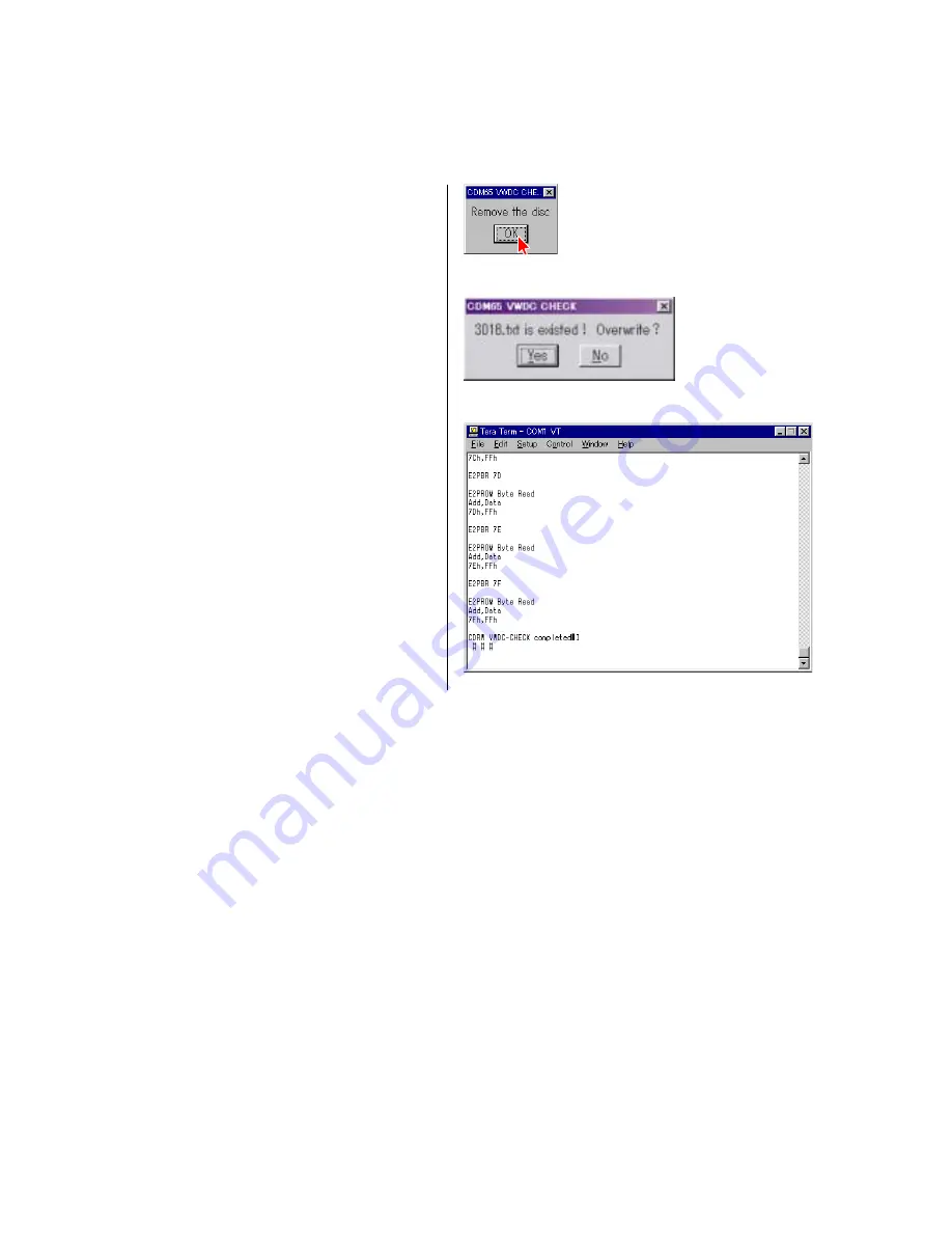
As prompted by the message shown in Fig. 4-51, remove the
disc from the tray and press “OK”.

3)

Because this step saves the result of electrical adjustment in a
file, there can be a case that the dialog as shown in Fig. 4-52
appears.

When you want to overwrite ..................... Press “Yes”.
When you want to create a new file .......... Press “No”.

4)

Check that the message “CDRW VWDC-CHECK completed!”
appears. 

(Fig. 4-53)

NG Judgment Result Indication

4

 Fig. 4-51

4

 Fig. 4-52

4

 Fig. 4-53

4-6-1.

EEPROM Write NG!

Contents : This message appears when writing data into EEPROM fails.
Measure : When the steps of 01ldp_S.ttl through 05cdrw_S.ttl have no problem and the error occurs only in this step, it is assumed that

an error has occurred momentarily in the interface between PC and CDM65. Therefore, repeat execution of 06vwdc_S.ttl
again.

4-6-2.

VWDC judge [Line Top - End] [NG]

Contents : This message appears when the VWDC value is outside the specification.
Measure : It is assumed that the optical laser unit has deteriorated. If this error occurs after the KRM-220CAA is replaced, the adjustment

error in the step of 01ldp_S.ttl is assumed. Therefore, repeat execution of steps of 01ldp_S.ttl through 05cdrw_S.ttl again. In
the cases other than above, check if the laser power adjustment is correctly performed or not, using LDPtestL_S.ttl.

Summary of Contents for RCD-W10 - Cd/cdr Recorder/player

Page 1: ...nm Emission duration continuous Playable discs CD CD R CD RW Recordable discs CD R CD RW for music use Frequency response 20 Hz 20 000 Hz 0 5 dB General Power requirements North American model 120 V AC 60 Hz Power consumption 25 W Dimensions approx w h d incl projecting parts and control 430 108 399 mm 17 4 3 8 15 3 4 inch Mass approx 6 0 kg 13 lbs 4 oz Supplied accessories Design and specificatio...

Page 2: ... LA SÉCURITÉ DE FONCTIONNEMENT NE REMPLACER CES COMPOSANTS QUE PAR DES PIÈSES SONY DONT LES NUMÉROS SONT DONNÉS DANS CE MANUEL OU DANS LES SUPPÉMENTS PUBLIÉS PAR SONY After correcting the original service problem perform the following safety checks before releasing the set to the customer Check the antenna terminals metal trim metallized knobs screws and all other exposed metal parts for AC leakag...

Page 3: ...68 6 14 Printed Wiring Board DISPLAY Section 69 6 15 Schematic Diagram DISPLAY Section 70 6 16 IC Block Diagrams 71 6 17 IC Pin Function Description 74 7 EXPLODED VIEWS 84 7 1 Case Section 84 7 2 Front Panel Section 85 7 3 Chassis Section 86 7 4 CDR Mechanism Deck Section CDM65 RBD1 87 7 5 CD Mechanism Deck Section CDM66C 30B61B 88 7 6 Base Unit Section BU 30BBD61B 89 8 ELECTRICAL PARTS LIST 90 Un...

Page 4: ...ack in DECK A or with an external device such as CD ROM or VIDEO CD Remove the disc and then insert a music CD for playback Recording has not been completed successfully because of vibration Relocate the unit in a place free of vibration and restart the recording again The disc you try to record is excessively dirty such as oil stained or finger marked or scratched Or the disc is not normal Replac...

Page 5: ...6 OPEN CLOSE A button 7 H button 8 INPUT button 9 FINALIZE button q ERASE button qa SBM button and indicator qs REC z button qd X button qf REC LEVEL knob qg x button qh PLAY MODE button qj TIME button qk DISPLAY button ql YES button w l AMS L knob wa CLEAR button ws MENU NO button wd l AMS L knob wf CLEAR button wg PLAY MODE button wh TIME button wj x button wk PHONES jack wl X button e PHONE LEV...

Page 6: ...G PANEL 1CD LOADING PANEL CDR DISPLAY BOARD CD MECHANISM DECK CDM66C 30B61B CDR MECHANISM DECK CDM65 RBD1 CDR BOARD HOLDER MG SUB ASSY DUST COVER TRAY CASE 409538 FRONT PANEL SECTION SET MOTOR ASSY LOADING M201 OPTICAL PICK UP KRM 220CAA TRAY 66 BD BOARD CAM CH MAIN BOARD OPTICAL BLOCK SECTION ...

Page 7: ...ven 3 1 Case 409538 3 2 Loading Panel 1CD 4 case 409538 3 two screws case 3 TP2 3 x 8 1 two screws case 3 TP2 3 x 8 2 two screws case 3 TP2 3 x 8 front panel side 1 Rotate the hole to the direction of arrow CD mechanism deck CDM66C 30B61B 4 2 3 two hooks 4 loading panel 1CD ...

Page 8: ...on of arrow 2 4 front panel side CD mechanism deck CDM65 RBD1 lever 3 two hooks 5 loading panel CDR 7 two claws 8 front panel section 1 connector 2 core CN900 2 connector 3 core CN690 4 connector 2 core CN920 5 three screws BVTP 3 8 6 four screws BVTP 3 8 3 flexible flat cable 21core CN671 ...

Page 9: ... 8 5 three screws BVTP 2 6 8 2 two knobs AMS 1 knob AMS 9 CD EJECT board 7 claw 8 Remove the soldering HARNESS PROCESSING q flexible flat cable 21core CN700 qa DISPLAY board 4 CD SW board POWER SW board 3 four screws BVTP 3 8 2 flexible flat cable 11core CN630 1 connector 4P CN631 4 CDR mechanism deck CDM65 RBD1 ...

Page 10: ...row 3 Pull the tray while pressing the claw of the chassis and the claw of the tray in the direction of the arrow front panel side lever cam CH claw claw claw chassis chassis tray 7 claw 6 claw 8 connector 2 core CN104 3 flexible flat cable 32core CN101 4 flexible flat cable 11core CN102 5 flexible flat cable 11core CN103 9 CDR board 2 bottom plate 1 four screws BVTP 2 6 8 ...

Page 11: ...KRM 220CAA 4 three screws BVTP 2 6 8 3 holder MG sub assy 1 two claws 2 two claws 5 dust cover 5 flexible flat cable 32core from optical device 1 two step screws 2 two screws 2X9 G with p tappin 6 optical pick up KRM 220CAA 3 two insulators main 4 two insulators main ...

Page 12: ...n of arrow 2 Remove the belt loading from the pulley of the motor assy 3 two claws 4 motor assy loading M201 1 1 1 1 6 screw PTPWH 2 6 8 5 holder BU sub assy cam CH claw 1 2 4 3 A qa q Slide the cam CH to the direction of arrow A while pressing the claw qs cam CH 7 gear C 9 gear B 8 claw ...

Page 13: ...13 RCD W10 3 13 CD Mechanism Deck CDM66C 30B61B 3 three screws BVTP 3 8 2 flexible flat cable 23core CN101 1connector 5P CN680 4 CD mechanism deck CDM66C 30B61B ...

Page 14: ...14 RCD W10 3 14 Tray 66 8 tray 66 3 hook 7 hook 6 hook 4 hook 2 5 1 Turn the cam to the direction of arrow ...

Page 15: ...l Block Section 1 Remove soldering from the four points 3 BD board 2 flexible flat cable 16core 1 floating screw 4 optical block section 3 shaft BU holder 2 Rotate the cam 66 in the direction of 2 to move the shaft BU holder upper cam 66 ...

Page 16: ...21core CN671 3 flexible flat cable 11core CN630 5 flexible flat cable 4core CN631 7 flexible flat cable 23core CN660 6 connector 5core CN680 qa two screws BVTT 3 6 q three screws BVTP 3 8 8 screw BVTP 3 8 qs four screws BVTT 3 6 qd Remove the soldering qg MAIN board qf power transformer 9 bracket TR ...

Page 17: ...17 RCD W10 MEMO ...

Page 18: ... DECK B knob to execute the Ship Mode 4 Press the POWER button to POWER off BU Test Mode Deck A Procedure 1 Enter the test mode then turn the l AMS L DECK B knob to display BU Test and press the l AMS L DECK B knob 2 bdt S CURVE is displayed This test mode is used in the Elec trical Adjustment section 3 Turn the l AMS L DECK B knob bdt RAM READ bdt RAMWRITE bdt COMOUT bdt FB TUNE and bdt ERR RATE ...

Page 19: ...n the l AMS L DECK B knob to display RM CHECK and press the l AMS L DECK B knob 2 Press the H key on the remote commander then Got PlayCom is displayed 3 Press the MENU NO button then RM CHECK is displayed again 4 To exit from this mode turn the l AMS L DECK B knob to display Ship Mode and press the l AMS L DECK B knob to execute the Ship Mode 5 Press the POWER button to POWER off CDR History Disp...

Page 20: ...peration of finalize 13 PMA erasing 14 emergency 15 recording preparation 16 recording end examples 4 Start time of read in compression method bit 15 to bit 13 min 0 97 min 1 96 min 2 95 min 7 others bit 12 to bit 7 sec bit 6 to bit 0 frame examples 0000 1101 1000 0000 0001 0001 0001 0110 0D 80 11 16 7 0 frame 6 5 4 3 2 1 34 sec 97 min 22 frame 0 15 14 13 12 11 10 9 8 Start time of read in 97 27 0...

Page 21: ... Note Try to measure several times to make sure than the ratio ofA B or B A is more than 10 7 RF Level Check Connection Procedure 1 Connect an oscilloscope to TP RFAC and TP DVC 2 Turn the power on 3 Load the disc YEDS 18 and playback the number five track 4 Confirm that oscilloscope waveform is clear and check RF signal level is correct or not CD SECTION DECK A Note A clear RF signal waveform mea...

Page 22: ...g of Programs 1 1 Connection Jig CONTROL FIRM RESET 0 756 358 11 CDM65 RBD1 SERVICE To RCD W10 CDM65 RBD1 Jig A B C D B C D Test Disc COM1 PC w SerialI F Laser Power Cables for Jig connecting Meter Oscilloscope MPXOUT RS 232C Cable 3 5 7 1 6 8 9 2 CDM65 RBD1 jig 4 Fig Position of Jig Set the jig after removing the cover of CDM65 RBD1 ...

Page 23: ...01 Parts No J 2501 046 A 7 Test Disc PATD 012 Parts No 4 225 203 1 Adjustment for Playback CD CD R TCD W091W Parts No J 2501 226 A Adjustment for Playback CD RW CRM74 Blank CD R Adjustment and Check for Recording CD R CWM74 Blank CD RW Check for Recording CD RW TCD W032W Parts No J 2501 227 A Defocus tolerance CD RW 8 RS 232C Cable 9 Cables for Jig connecting PH 5p PH 4p FFC 11p 1 0mm pitch J 2501...

Page 24: ...he serial port from OS a Select Start Settings Control Panel and select System Device manager Communication Port COMn see Fig 1 1 Specify the COM port that connected with JIG of CDM65 b Double click COMn as you connect to the Jig CDM65 Set the parameters as below Bits per second 38400 Data bits 8 Parity non Stop bits 1 Flow control hardware see Fig 1 2 4 Fig 1 1 4 Fig 1 2 ...

Page 25: ...ttl file and FUNC folder which are contained in files 0208 and paste them in the Ttermpro file as below The file files 0208 zip is distributed together with the service manual Note Do not change the directory path 5 Start up the TeraTermPro Double click the ttermpro exe 6 Set up the TeraTermPro IMPORTANT a Select Setup Serial Port and set the parameters as below Port As you connect to the Jig CDM6...

Page 26: ...up Select Setup Save setup and save as teraterm ini in the Ttermpro directory see Fig 1 8 4 Fig 1 6 4 Fig 1 7 4 Fig 1 8 4 Fig 1 9 7 Connect the JIG and CDM65 8 Confirm the S510 on JIG is CONTROL 9 Power on the CDM65 and press SW101 RESET on JIG CDM65 RBD1 has connected with this PC is displayed see Fig 1 9 If above message is not displayed you may have some mistakes Please confirm previous setting...

Page 27: ...r works as shown below electrical adjustment is required KRM 220CAA is replaced RBD1 is replaced The parts shown in the List 1 is replaced Locating the faulty point Electrical adjustment Electrical adjustment is not required List 1 IC101 IC103 IC171 IC201 IC502 Yes Yes Yes No No No ...

Page 28: ...Place probe of a laser power meter in the specified position following the display as shown in Fig 3 3 See Fig 3 3 a jig CDM65 RBD1 optical pick up sensor probe 4 Fig 3 3 a 3 Locating the Faulty Point 3 1 Laser Power Check 2 Press the RESET button SW101 of the jig as prompted by the display Note Do not add stress to an optical pick up ...

Page 29: ... display shown in Fig 3 6 appears set the Range of a laser power meter to 10 mW and press OK 7 Check that the laser power meter reading satisfies the following requirement When the laser power satisfies the required specification press OK Fig 3 7 LEADER LPM 8001 4 5 to 4 7 mW 8 Check that the laser power meter reading satisfies the following requirement When the laser power satisfies the required ...

Page 30: ...erioration Judgment 1 Select the menu as follows Control Macro and select 10vwdcC_S ttl Press Open Fig 3 10 3 11 4 Fig 3 9 4 Fig 3 10 4 Fig 3 11 2 Press the RESET button SW101 of the jig as prompted by the display 3 When the message OK appears as shown in Fig 3 12 press the OK button When the laser unit KRM 220CAA Op is normal without deterioration of laser the message OK appears If the laser unit...

Page 31: ...lowing the Connection Diagram as shown in section 1 1 2 Turn on the power of the RCD W10 in which the CDM65 is installed 3 Start up the TeraTermPro that is installed in PC Set the switch S510 on the jig to CONTROL 4 Press the RESET button SW101 of the jig Fig 3 14 5 Type portchk Enter from keyboard of PC Fig 3 15 Note 5 1 When the KRM 220CAA is connected the spindle motor rotates at a high speed I...

Page 32: ... Fig 3 16 is defective or its peripheral has abnormality Perform the repair work again and repeat the self diagnosis Repeat the repair work and self diagnosis until OK is displayed 4 Fig 3 16 7 Perform the operation check 3 4 Use of Self Diagnosis Function 2 In the case when result data of the past electrical adjustment should be left saved Perform the self diagnosis as described below in the case...

Page 33: ...ed up Fig 3 20 4 Fig 3 19 4 Fig 3 20 4 Perform step 1 through step 6 of section 3 3 Use of Self Diagnosis Function 1 5 Select the menu as follows Control Macro and select E2recvF ttl Press Open 6 Press the RESET button SW101 of the jig as prompted by the display Fig 3 21 7 Type the filename in which result of electrical adjustment is saved Press OK Fig 3 22 4 Fig 3 21 4 Fig 3 22 ...

Page 34: ...ition of Elapsed Operating Hours Check if error has occurred or not by performing the following steps If error has occurred it is interpreted and saved in the specific directory Check contents of the error by viewing the specific directory as described below 1 Select the menu as follows Control Macro and select ErrHistGetAll_S ttl Press Open Fig 3 24 3 25 4 Fig 3 24 4 Fig 3 25 ...

Page 35: ...ry 5 The elapsed operating hours is shown at the top of EEPROM_Errorlog txt regardless of presence absence of the error history Check the elapsed operating hours from the display as shown in Fig 3 28 4 Fig 3 26 4 Fig 3 27 4 Fig 3 28 Error log example SN xxxx Op elapsed time 12 0 56 Spindle elapsed time 17 9 44 Error Log data 0 Error Pointer 38 Error Code 05 04 E0 00 00 01 0D 0D Focus is dropped 1x...

Page 36: ...W101 of the jig as prompted by the display 4 Press the RESET button SW101 of the jig again as prompted by the display 5 When the display as shown in Fig 4 2 appears type the serial number see Fig 4 3 that is printed on the label attached to the RBD1 This dialog appears only when the EEPROM IC502 is replaced When the display as shown in Fig 4 4 appears press No When the display as shown in Fig 4 5 ...

Page 37: ... LEADER LPM 8001 0 81 0 05 mW 0 76 to 0 86 mW To increase the laser output power Press Yes of the Up dialog box To decrease the laser output power Press No of the Up dialog box and then press Yes of the Down dialog box Repeat until the laser output power satisfies the specification Fig 4 8 4 9 When the setting value is determined Press No of the Up dialog box and then press No of the Down dialog b...

Page 38: ...s No of the Down dialog box and press Yes of the Save dialog box Fig 4 14 11 Adjust the laser output power as follows The laser output power i e laser power meter reading should satisfy the specification shown below LEADER LPM 8001 9 4 0 2 mW 9 2 to 9 6 mW To increase the laser output power Press Yes of the Up dialog box To decrease the laser output power Press No of the Up dialog box and then pre...

Page 39: ...1 peripheral and the sled drive mechanism 4 1 2 Power CAL NG Contents This message appears when the laser emission intensity is outside the specification Measure Check peripheral of CN101 Replace KRM 220CAA 4 2 CD CD R Playback Adjustment 1 Select the menu as follows Control Macro and select 02cdr_S ttl Press Open 2 Place the test CD disc PATD 012 on the tray as prompted by the display and press O...

Page 40: ... center of the waveform RF signal waveform VOLT DIV suitable value TIME DIV 500ns 4 Fig 4 22 RF signal waveform VOLT DIV suitable value TIME DIV 500ns 4 Fig 4 23 RF signal waveform VOLT DIV suitable value TIME DIV 500ns 4 Fig 4 25 4 Fig 4 24 4 Fig 4 26 7 Check that the message CDR PB CAL completed appears NG Judgment Result Indication 4 2 1 Playback Measurement NG Contents This message appears whe...

Page 41: ...that the waveform as shown in Fig 4 28 appears on an oscilloscope 5 As prompted by the message shown in Fig 4 31 check that the waveform as shown in Fig 4 30 appears on an oscilloscope 6 As prompted by the message shown in Fig 4 33 check that the waveform as shown in Fig 4 32 appears on an oscilloscope 4 Fig 4 29 RF signal waveform VOLT DIV suitable value TIME DIV 500ns 4 Fig 4 28 4 Fig 4 31 RF si...

Page 42: ...that is used by this step cannot be used for the general purposes and for the purpose of operation check of the RCD series equipment The disc that is used for the general purposes or for the purpose of operation check of the RCD series equipment cannot be used in this step If the recording is interrupted by any reasons during the recording operation i e the WRITE POWER ON LED of the jig is lightin...

Page 43: ...prompted by the message shown in Fig 4 42 check that the waveform as shown in Fig 4 41 appears on an oscilloscope 4 Fig 4 37 4 Fig 4 38 4 Fig 4 40 4 Fig 4 42 RF signal waveform VOLT DIV suitable value TIME DIV 500ns 4 Fig 4 39 RF signal waveform VOLT DIV suitable value TIME DIV 500ns 4 Fig 4 41 8 Check that the message CDR REC CHECK completed appears NG Judgment Result Indication 4 4 1 CD R Playba...

Page 44: ...sc If the recording is interrupted by any reasons during the recording operation i e the WRITE POWER ON LED of the jig is lighting the disc cannot be used any more in the subsequent step In such a case erase the CD RW disc and repeat this step from the very beginning again 3 When the disc that is used in step 2 is the disc that has been used in the electrical adjustment in the past Press Yes When ...

Page 45: ...t the waveform as shown in Fig 4 49 appears on an oscilloscope 8 Check that the message CDRW REC CHECK completed appears Fig 4 50 NG Judgment Result Indication 4 5 1 CD RW Playback Measurement NG Contents This message appears when the BLER Block Error Rate Beta m11 of the track that is recorded and played back is outside the specification Measure Check if there is any abnormality in RBD1 Replace K...

Page 46: ...e appears when writing data into EEPROM fails Measure When the steps of 01ldp_S ttl through 05cdrw_S ttl have no problem and the error occurs only in this step it is assumed that an error has occurred momentarily in the interface between PC and CDM65 Therefore repeat execution of 06vwdc_S ttl again 4 6 2 VWDC judge Line Top End NG Contents This message appears when the VWDC value is outside the sp...

Page 47: ...ustment has not completed within the specified time RPINWADJ2 NG The Read Power during Write2 Adjustment has not completed within the specified time SERVOSET NG The Servo Setting has not completed within the specified time TSa NG The ATIME Search has not completed within the specified time PLAYSW NG The Play operation has not started within the specified time STOP NG The Stop operation has not com...

Page 48: ... History 1 Select the menu as follows Control Macro and select ErrHistClear ttl Press Open Fig 5 1 5 2 4 Fig 5 1 4 Fig 5 2 2 Press the RESET button SW101 of the jig as prompted by the display 3 Check that the message completed appears Fig 5 3 4 Fig 5 3 ...

Page 49: ...and install the TCD W032W in Deck B 2 Rotate the l AMS L Deck B knob to select the track 16 Start playback by pressing the same knob or by pressing the H Deck B button 3 Perform playback for 10 seconds or more and confirm that there is no abnormality such as sound skipping and others ...

Page 50: ...ustment or to use a disc other than blank Be sure to erase it in the following procedure to use the disc used for electrical adjustment for other uses 4 Fig A 1 4 Fig A 2 4 Fig A 3 1 Select the menu as follows Control Macro and select RWeraseA ttl Press Open Fig A 1 A 2 2 Press the RESET button SW101 of the jig as prompted by the display Fig A 3 ...

Page 51: ...wn by the arrow mark in Fig A 4 is updated after a while 4 Fig A 4 4 When update of time display is stopped and rotation of spindle is stopped press the STOP button SW501 of the Jig and then press the EJECT button SW508 of the jig to remove the disc ...

Page 52: ...52 RCD W10 MEMO ...

Page 53: ... The other layers patterns are not indicated Indication of transistor THIS NOTE IS COMMON FOR PRINTED WIRING BOARDS AND SCHEMATIC DIAGRAMS In addition to this necessary note is printed in each block Note The components identified by mark 0 or dotted line with mark 0 are critical for safety Replace only with part number specified Note Les composants identifiés par une marque 0 sont critiques pour l...

Page 54: ...OUT XTAL 67 EXTAL 66 X501 20MHz 1 2 4 1 2 7 IC504 5V D SDATAI HOST 15 1 2 4 IC506 XREQI 7 IC505 6 5 3 IC505 SDATAO HOST 13 XRDYO 8 5V D XREST 63 XMMUTE 96 TMP 84 SLFG 93 Q170 A SDATAI HOST SDATAO HOST XREQ RESET REV 99 FWD 100 XRDY DIN1 11 10 IC301 9 8 IC301 DIN2 1 2 IC301 13 12 IC301 1 2 4 IC302 5V D DOUT IC103 IC104 2 4 IC150 GATE 21 MIRR XRC 2 95 SPFG 78 KEY KEY PCIFE XFIRM 4 2 IC204 34MHz EFM ...

Page 55: ...ADING 7 SENS SENSE 18 RFAC 50 15 RFAC 26 RFC PWM1 12 PWM2 19 PWM3 20 23 IN4 2 4 IC105 69 XTSL CTRL1 1 2 1 4 SQCLK 17 LOD_NEG 55 LOD_POS 54 OUT_SW 52 6 CD R IN 7 CD R OUT 28 XRDY 33 XREQ 3 DA DATA IN A D D A CONV IC500 RX2 44 13 TX1 CDTO 9 4 DA DATA OUT CDTI 8 5 DA CLK CCLK 10 8 DA LATCH CS 11 25 DA RESET PDOWN 5 67 DZF DZF 30 94 INT0 INT0 6 95 INT1 INT1 7 TX3 16 RX4 4 DIGITAL IN OPTICAL IC610 DIGI...

Page 56: ...V RV780 S1701 DECK A CD JOG 0 68 ENCODER 1 4 S723 CD JOG 1 69 3 FUNCTION KEY S720 722 KEY 1 78 FUNCTION KEY S718 719 R JOG 0 70 ENCODER 1 4 S717 R JOG 1 71 3 FUNCTION KEY S710 716 KEY 0 77 FUNCTION KEY S700 704 POWER DOWN IC476 D431 434 TR900 S921 POWER SW AC IN RESET IC480 2 1 AC AC TO CD R LINE FILTER LF900 36V REG IC460 1 3 36V D461 7V REG IC440 1 3 D451 454 8V REG IC430 1 3 CD 8V CD 7V 8V REG ...

Page 57: ...s unleaded solder See page 53 for Circuit Boards Location IC201 IC101 IC104 IC102 IC103 IC105 C 1 3 A MAX 3 Page 65 MAIN TP RFAC TP DVC TP TE TP FE Ref No Location IC101 B 2 IC102 C 1 IC103 B 3 IC104 C 2 IC105 B 7 IC201 A 2 Q101 A 3 Semiconductor Location ...

Page 58: ... R105 R104 C103 R112 C107 R120 R116 C117 R114 R113 C109 R126 R125 C110 C108 R122 R124 R123 C114 C119 C118 C219 C222 R219 C234 C235 C236 R227 R228 R229 R152 R151 C151 C152 R178 R179 R177 C171 C167 C179 C178 C164 R165 R166 R168 R170 C232 C169 C168 C166 R115 CN101 TP49 TP TP TP X201 CXD3068Q BA033FP E2 47k 47 4V 47 4V 100 4V 47 6 3V 47 4V 100 16V 10 16V 100 10V 220 4V 100 10V MC74VHC1G0 4DFT1 TC74HC4...

Page 59: ...ng Board CD R Section Side A See page 53 for Circuit Boards Location IC 150 IC 102 IC 104 IC 202 IC 502 LASER POWER METER 66 65 TO JIG NOT USED Ref No Location IC102 B 5 IC104 A 6 IC150 B 4 IC202 D 6 IC502 D 5 Semiconductor Location ...

Page 60: ... IC 201 IC 501 IC 101 IC 301 IC 504 IC 171 IC 172 IC 506 IC 505 IC 302 IC 110 IC 103 IC 204 1 2 Ref No Location D101 C 6 D102 C 6 IC101 C 5 IC103 A 5 IC110 B 1 IC171 E 6 IC172 E 7 IC201 C 3 IC204 A 3 IC301 C 1 IC302 B 1 IC501 E 4 IC504 E 2 IC505 F 2 IC506 E 2 Q170 F 7 Q501 E 3 Semiconductor Location ...

Page 61: ...TP143 TP142 TP269 TP141 C139 C140 R157 CN121 TP184 TP186 TP197 TP200 TP201 R101 R102 R103 R126 TP105 C126 C122 6 3V VREF 5V RF VWDC1 FCS TRK TRK FCS OP E OP C OP D OP G OP H OP A OP B OP F TZC DFCT MIRR ATFG AK8567 6 3V FPD VC FGND RRFTOP RRFBTM MPP AGCON GAINUP RECD1 34MHZ RFPDSH AGND NM ATFM 16V B 10V B 16V B 16V B 6 3V B 3225 OP ENBL 16V B 25V B 1000p 50V B 1000p 50V B MPDSH 10V B AUX3 25V F PM...

Page 62: ...P202 TP536 R545 R555 C508 C513 R511 R533 R548 L503 R350 C301 TP350 TP349 C304 C302 R356 C303 R370 R369 C526 L501 TP506 RB520 1k BLM21P600SG 2012 BLM21P600SG 2012 BLM21P600SG 2012 16V 25V F 25V F 6 3V 25V F 6 3V 8V 5V D DGND 5V A AGND MGND 25V F 25V F 25V F 0 0 0 0 2 2k 100k 100k 3216 100k 3216 100k 3216 100k 3216 100k 3216 100k 3216 100k 3216 100k 3216 100k 3216 100k 3216 100k 3216 100k 3216 100k ...

Page 63: ... 4 IC103 3 4 IC103 4 4 IC104 C156 TP205 TP204 TP239 TP207 TP236 C191 C192 S170 S171 CN102 TP118 TP121 R189 R190 CN103 CN104 R198 C186 R193 C188 C189 C190 R176 R194 BA5937AFP LB11698H 16V 10 10 10 220 E 16V 25V F 25V F 25V F 25V F 25V F SLED SLED 10k 0 0 0 SPFG 33k E 22k E SLFG LMO LMO LOAD_IN LOAD_OUT 2 5V 1 2 5V 2 4 7k E 6 8k E 10k E 10k E ENCO XMMMUTE 0 DTC114EKA 10k 0 MGND DGND 6 3V 6 3V 16V 25...

Page 64: ... R248 C225 C227 C224 R250 TP331 TP330 TP365 TP322 TP323 C259 C241 TP221 TP220 R305 TP324 TP325 TP179 C260 C237 R269 TP165 TP222 TP358 TP280 TP286 C239 R270 R267 C240 C246 C218 R240 R227 TP359 C251 R251 C206 C234 R262 R263 R231 R283 R212 LC89587 UK1 MSM54V16258BSL 40TSK 25V F 15k E 220 16V B 16V B 25V F 6 8k E 6 8k E 6800p 25V B 680p 50V B 25V F 5 6k E 25V F 0 MON2 MON4 16V B 75 5 6k E 5 1k E 680 E...

Page 65: ...C 100 IC 1 IC 500 IC 370 IC 310 IC 390 IC 476 IC 480 C802 D805 69 59 57 Ref No Location D181 B 3 D310 E 2 D311 E 1 D316 E 1 D426 C 2 D462 C 5 D471 C 5 D472 C 6 D473 B 6 D805 B 7 IC1 B 2 IC100 B 1 IC310 F 1 IC370 F 2 IC390 F 3 IC476 C 6 IC480 B 7 IC500 D 1 Q181 F 2 Q191 E 3 Q281 F 2 Q291 E 3 Q380 B 3 Semiconductor Location ...

Page 66: ... LOADING 9 10 11 CN680 C805 1 1 8 5 M S272 LOADING IN S271 LOADING OUT 1 645 721 21 21 LOADING BOARD 69 59 69 Ref No Location D401 D 4 D402 D 4 D403 D 4 D404 D 4 D411 E 4 D412 E 4 D421 D 4 D422 D 4 D431 F 4 D432 E 4 D433 E 4 D434 E 4 D451 F 3 D452 F 3 D453 F 3 D454 F 3 D461 D 4 IC410 F 3 IC420 D 5 IC430 F 4 IC440 F 5 IC450 F 2 IC460 C 4 IC610 F 6 IC620 F 5 IC800 A 2 Q310 E 7 Semiconductor Location...

Page 67: ...5 R550 C630 CN1 R500 D426 R540 R12 R19 R20 C12 C19 C76 R88 C20 R516 R636 RB77 RB68 RB54 RB51 RB47 RB43 X38 IC500 D311 D316 R513 R107 IC1 C805 D805 C802 IC800 CN680 CN151 S272 S271 M151 0 0 0 0 0 0 0 001 0 1 0 1 0 1 0 1 0 1 0 1 0 1 0 1 0 1 0 1 0 1 0 1 1 50V 100 16V 100 16V 100 16V 100 16V 100 100 100 100 100 100 100k 100k 10k 10k 10k 10k 10k 10k 10k 10k 10k 10k 10k 1SS181 4 7k 21P BR24C02FV W 11P U...

Page 68: ...34 D453 D451 D454 D452 D411 D412 D421 D422 D401 D402 D403 D404 IC620 IC610 M5293L 100 63V 1000 16V 1000 16V 4700 25V AN7807 100k 220 220 47 50V 1000 10V 1000 10V 1000 10V 1000 10V 1000 10V 470p 470p 470p 330 330 470p 33k 22k 33k 22k 47 220k 220k NJM4565V 2SD1938 2SD1938 10k 10k 0 NJM4558V 680 100k 100k 680 10k 10k 23P 1SS355 1SS355 470 470 1SS355 22k 22 25V 4700 25V 47k 0 150k 1k 100k 2P 2200p 220...

Page 69: ...ring Board DISPLAY Section See page 53 for Circuit Boards Location Uses unleaded solder IC 781 IC 760 3 4 1 2 65 66 66 Ref No Location D775 F 1 IC760 G 9 IC781 G 13 Semiconductor Location Ref No Location Q761 G 6 Q762 G 6 Q775 G 3 ...

Page 70: ...711 R721 R775 R702 R712 R722 R718 R703 R713 R723 R704 R714 R724 J790 CN920 CN700 S921 IC781 IC760 CN725 CN720 CN921 EP720 RV780 EP780 FL750 EP750 C742 R766 C767 C770 C769 C768 C766 S723 RV790 CN710 S1701 R1701 CN1780 L1790 100k 100k 100 100 0 001 0 001 10 50V 10 50V 2SC2603TP 2SC2603TP UN4211 SEL5821A TP15 100 47 470p 470p WIRE 3P 10 10 JW 100 100 100 100 0 1 50V ENCORDER 2200p 1k 1 5k 2 2k 4 7k 1...

Page 71: ...RR SE FE VC TES1 TEST FFDR TRDR TFDR SRDR SFDR FSTO SSTP LOCK PWMI FOK FRDR MDP DFCT CLOCK GENERATOR ASYMMETRY CORRECTOR DIGITAL PLL CPU INTERFACE INTERFACE CORRECTOR PROCESSOR SUB CODE RAM 32K DEMODURATOR EFM ERROR D A DIGITAL OUT INTERFACE SERVO INTERFACE SERVO AUTO MIRR DFCT FOK SERVO FOCUS SERVO DSP SERVO SERVO SLED TRACKING FOCUS PWM GENERATOR GENERATOR GENERATOR SLED PWM TRACKING PWM A D CON...

Page 72: ...2 17 18 15 16 19 20 21 1 2 3 4 5 6 7 12 11 14 13 10 9 8 D D D D x2 x2 x2 x1 4 D x2 D IC172 LB11698H TE L CDR Board 18 17 16 19 20 21 22 23 24 25 26 27 28 CURRENT LIMITER WAVEFORM DISTRIBUTER FORWARD REVERSE REVERSE BRAKE SWITCH FUNCTION SHORT BRAKE REFERENCE VOLTAGE THERMAL SHUTDOWN CURRENT LIMITER CONTROL 1 HALL FG 3 HALL FG HALL POWER SUPPLY ROTATION DIRECTION DETECTOR MATRIX RF VCC2 UOUT VOUT W...

Page 73: ...MCLK R_LRCK R_BICK R_DATA R_MCLK D_LRCK D_BICK D_DATA D_MCLK A_LRCK A_BICK A_DATA A_MCLK S_LRCK S_BICK S_DATAI S_DATAO MCKI IC760 MSM9201 04GS K DISPLAY Board SEGMENT DRIVER AD DRIVER 80 2 AD4 1 AD3 COM2 COM1 VDISP1 AD2 79 AD1 PORT DRIVER COMMAND DECODER WRITE ADDRESS COUNTER ADDRESS SELECTION DCRAM ADDRESS COUNTER READ ADDRESS COUNTER 8 bit SHIFT REGISTER OSCILLATOR TIMING GENERATOR1 TIMING GENER...

Page 74: ...nal output to FE SIRCS signal input from the remote control receiver Laser ON signal output Sub code Q serial data input Not used open Sub code Q output serial clock output SENSE signal input from the IC101 PWM signal output toTE PWM signal output to RFDC Flash programming power supply Not used open Disc rotation speed selection signal output Disc rotation speed selection signal output Reset signa...

Page 75: ... used Power supply 5V Ground terminal Not used open EEPROM I2C data input output EEPROM I2C clock output EEPROM write protect signal output Reset signal output to the FL driver Zero data detect signal input from the AD DA converter IC500 CD jog signal input CD jog signal input CD R jog signal input CD R jog signal input Chip select signal output to the FL driver Strobe signal output to the LED dri...

Page 76: ...Laser monitor voltage input Power setting voltage input for read APC internal DAC setting voltage output Read laser driver control signal output Read laser driver control amplifier teminal Read laser driver time constant setting terminal Power setting voltage input for write APC internal DAC setting voltage output Power setting internal DAC voltage output for write APC Not used open Power supply a...

Page 77: ...measuring circuit reset signal input H reset the outputs of PHBETA and BHBETA Clock input for register setting Serial data input for register setting Latch siganl input for register setting Register reset terminal L reset Ground terminal analog Capacitor connection terminal for setting fc of the equalizer output offset canceller External capacitor connection terminal for setting the RFAGC response...

Page 78: ...ATA signal open Monitor output CDETR CK2 signal Monitor output EMP LRCK signal open Power supply 5V digital Ground terminal digital ENCERR signal output pull up TESTOUT signal output pull up TESTIN signal input ground Write strategy signal control terminal Servo sampling pulse output Servo sampling pulse output Laser sampling pulse output Laser sampling pulse output Running OPC sampling pulse outp...

Page 79: ...t terminal P N balance adjustment terminal Charge pump terminal for the frequency comparison Charge pump terminal for the phase comparison Filter for the charge pump Power supply 3 3V analog for the charge pump Ground terminal analog Charge pump selection terminal Not used open VCO frequency setting input teminal AD input FOK signal input for optical judgement Focus error signal input Tracking err...

Page 80: ... 3V analog for the clock jitter suppressor VCO gain control signal input VCO free running oscillation frequency control signal input Loop filter setting terminal Power supply 3 3V analog for the DIR Ground terminal analog Power supply 5V digital Ground terminal digital PLL lock data error output Digital data input from the IC500 Digital data input from the IC101 Digital data input Not used open DA...

Page 81: ...t fixed at L Sub code I F serial data input output fixed at L Sub code I F data shift clock input output fixed at L Sub code I F frame sync signal input output fixed at L Sub code I F block sync signal input output fixed at L Row address strobe signal output to the buffer RAM for audio data delay Column address strobe signal output to the buffer RAM for audio data delay Write enable signal output ...

Page 82: ...ata input from the IC502 Serial data input from the IC1 Clock output to the IC101 and IC502 Sub code sync signal input from the IC201 β measurement circuit reset signal output Not used fixed at H MIRR or RC selection signal output Ground terminal AGC enable signal output to the IC101 CD RW selection signal output to the IC101 Read laser driver time constant selection switch control signal output t...

Page 83: ...nput from the IC101 THERMOUT signal input VWDC2 signal output to the optical pick up Ground terminal for the A D converter Interrupt request signal input from the IC201 Recorded block detection signal input from the IC101 Tracking failure detection signal input from the IC101 Not used RS 232C H detection signal input Ground terminal ENCOUT signal input Tracking zero cross detection signal input fr...

Page 84: ...with mark 0 are critical for safety Replace only with part number specified Les composants identifiés par une marque 0 sont critiques pour la sécurité Ne les remplacer que par une pièce portant le numéro spécifié SECTION 7 EXPLODED VIEWS 84 RCD W10 Ref No Part No Description Remarks Ref No Part No Description Remarks 7 1 Case Section 1 4 238 393 01 PANEL CDR LOADING 2 4 238 905 01 PANEL 1CD LOADIN...

Page 85: ... KNOB AMS 55 4 231 973 01 BUTTON POWER 56 1 683 869 11 POWER SW BOARD 57 4 951 620 01 SCREW 2 6X8 BVTP 58 3 931 378 51 KNOB F10 59 1 683 868 11 HP BOARD 60 1 685 605 11 CD EJECT BOARD 61 1 683 867 11 CD SW BOARD 62 A 4728 267 A DISPLAY BOARD COMPLETE 63 1 823 923 11 WIRE FLAT TYPE 21 CORE 64 3 354 981 11 SPRING SUS RING 51 52 55 56 57 57 57 57 58 59 60 61 62 63 57 not supplied not supplied 53 54 6...

Page 86: ...3 922 11 WIRE FLAT TYPE 11 CORE 0T900 1 437 623 11 TRANSFORMER POWER 1 7 685 646 79 SCREW BVTP 3X8 TYPE2 IT 3 5 7 685 871 01 SCREW BVTT 3X6 S CD mechanism deck section CDM66C 30B61B CDR mechanism deck section CDM65 RBD1 1 5 5 5 1 T900 101 102 103 102 103 104 106 108 101 not supplied 105 107 1 1 not supplied The components identified by mark 0 or dotted line with mark 0 are critical for safety Repl...

Page 87: ...ADING 514 4 237 176 02 PULLEY CG 515 4 237 177 02 GEAR A 516 4 237 178 02 GEAR B 517 4 237 179 02 GEAR C 518 4 237 180 01 CAM CH 519 4 237 182 01 CHASSIS 520 A 4727 459 A CDR BOARD COMPLETE 521 3 341 549 01 SCREW 2 6X8 DIA 7 5 PTP WH 522 4 240 987 01 SHEET DR 523 4 232 682 01 CUSHION 66 M201 A 4735 557 A MOTOR ASSY LOADING 501 502 503 505 506 508 509 510 511 518 512 517 519 520 521 516 515 513 514...

Page 88: ...561 4 228 414 01 BRACKET YOKE 562 X 4954 474 1 PULLEY ASSY CHUCKING 563 A 4604 363 A MOTOR L ASSY LOADING 564 1 645 721 11 LOADING BOARD 565 4 227 899 01 SCREW DIA 12 FLOATING 566 4 238 369 02 HOLDER BU 567 4 240 820 01 INSULATOR B BU 30B 568 4 238 372 01 SPRING INSULATOR COMPRESSION 569 4 985 672 01 SCREW PTPWH M2 6 FLOATING M151 1 763 790 11 MOTOR DC LOADING 2 7 621 775 10 SCREW B 2 6X4 3 7 685 ...

Page 89: ... Base Unit Section BU 30BBD61B Ref No Part No Description Remarks Ref No Part No Description Remarks 601 A 4727 463 A BD BOARD COMPLETE 602 1 782 817 11 WIRE FLAT TYPE 16 CORE 601 602 603 603 A 4735 885 A BU 30B ASSY ...

Page 90: ... 681 11 ELECT CHIP 100uF 20 00 16V C164 1 164 360 11 CERAMIC CHIP 0 1uF 16V C165 1 124 779 00 ELECT CHIP 10uF 20 16V C166 1 164 360 11 CERAMIC CHIP 0 1uF 16V C167 1 162 927 11 CERAMIC CHIP 100PF 5 50V C168 1 164 360 11 CERAMIC CHIP 0 1uF 16V C169 1 164 360 11 CERAMIC CHIP 0 1uF 16V C171 1 162 970 11 CERAMIC CHIP 0 01uF 10 25V C178 1 164 360 11 CERAMIC CHIP 0 1uF 16V C179 1 164 360 11 CERAMIC CHIP ...

Page 91: ... METAL CHIP 100 5 1 16W R227 1 216 839 11 METAL CHIP 33K 5 1 16W R228 1 216 849 11 METAL CHIP 220K 5 1 16W R229 1 216 819 11 METAL CHIP 680 5 1 16W R230 1 216 864 11 METAL CHIP 0 5 1 16W R234 1 216 809 11 METAL CHIP 100 5 1 16W NETWORK RESISTOR RN201 1 233 576 11 RES CHIP NETWORK 100 RN202 1 233 576 11 RES CHIP NETWORK 100 VARIABLE RESISTOR RV101 1 223 997 21 RES CARBON ADJ VAR 47K VIBRATOR X201 1...

Page 92: ... CERAMIC CHIP 0 1uF 25V C222 1 164 156 11 CERAMIC CHIP 0 1uF 25V C223 1 164 677 11 CERAMIC CHIP 0 033uF 10 00 16V C224 1 107 826 11 CERAMIC CHIP 0 1uF 10 00 16V C225 1 107 826 11 CERAMIC CHIP 0 1uF 10 00 16V C226 1 107 826 11 CERAMIC CHIP 0 1uF 10 00 16V C227 1 162 912 11 CERAMIC CHIP 7PF 0 5PF 50V C228 1 162 969 11 CERAMIC CHIP 0 0068uF 10 25V C230 1 162 912 11 CERAMIC CHIP 7PF 0 5PF 50V C232 1 1...

Page 93: ... 216 809 11 METAL CHIP 100 5 1 16W R102 1 216 809 11 METAL CHIP 100 5 1 16W R103 1 216 809 11 METAL CHIP 100 5 1 16W R104 1 218 871 11 METAL CHIP 10K 0 5 1 10W R105 1 216 864 11 METAL CHIP 0 5 1 16W R106 1 216 829 11 METAL CHIP 4 7K 5 1 16W R107 1 216 857 11 METAL CHIP 1M 5 1 16W R108 1 216 809 11 METAL CHIP 100 5 1 16W R109 1 216 809 11 METAL CHIP 100 5 1 16W R110 1 216 809 11 METAL CHIP 100 5 1 ...

Page 94: ...CHIP 10 5 1 16W R265 1 218 833 11 METAL CHIP 270 0 5 1 10W R267 1 218 883 11 METAL CHIP 33K 0 5 1 10W R268 1 218 864 11 METAL CHIP 5 1K 0 5 1 10W R269 1 216 817 11 METAL CHIP 470 5 1 16W R270 1 218 847 11 METAL CHIP 1K 0 5 1 10W R271 1 218 865 11 METAL CHIP 5 6K 0 5 1 10W R274 1 218 871 11 METAL CHIP 10K 0 5 1 10W R276 1 218 843 11 METAL CHIP 680 0 5 1 10W R277 1 218 865 11 METAL CHIP 5 6K 0 5 1 1...

Page 95: ...3216 SWITCH S170 1 786 288 11 SWITCH DETECTION LOAD IN SW S171 1 786 288 11 SWITCH DETECTION LOAD OUT SW VIBRATOR X201 1 795 519 11 VIBRATOR CRYSTAL 33 8688MHz X501 1 795 622 21 VIBRATOR CERAMIC 20MHz 1 683 867 11 CD SW BOARD CAPACITOR C720 1 164 159 11 CERAMIC 0 1uF 50V RESISTOR R725 1 249 417 11 CARBON 1K 5 1 4W F R726 1 249 419 11 CARBON 1 5K 5 1 4W F R727 1 249 421 11 CARBON 2 2K 5 1 4W F R728...

Page 96: ...75 21 SWITCH KEYBOARD DISPLAY S716 1 762 875 21 SWITCH KEYBOARD YES S717 1 475 235 31 ENCODER ROTARY AMS PUSH ENTER S718 1 762 875 21 SWITCH KEYBOARD MENU NO S719 1 762 875 21 SWITCH KEYBOARD CLEAR S720 1 762 875 21 SWITCH KEYBOARD OPEN CLOSE A S721 1 762 875 21 SWITCH KEYBOARD CD SYNCHRO NORMAL S722 1 762 875 21 SWITCH KEYBOARD CD SYNCHRO HIGH S723 1 475 235 31 ENCODER ROTARY AMS PUSH ENTER S724 ...

Page 97: ... 156 11 CERAMIC CHIP 0 1uF 25V C534 1 164 156 11 CERAMIC CHIP 0 1uF 25V C535 1 126 933 11 ELECT 100uF 20 00 16V C539 1 126 933 11 ELECT 100uF 20 00 16V C541 1 164 156 11 CERAMIC CHIP 0 1uF 25V C600 1 126 963 11 ELECT 4 7uF 20 00 50V C611 1 164 156 11 CERAMIC CHIP 0 1uF 25V C621 1 164 156 11 CERAMIC CHIP 0 1uF 25V C630 1 216 864 11 METAL CHIP 0 5 1 16W C670 1 164 156 11 CERAMIC CHIP 0 1uF 25V C802 ...

Page 98: ...L CHIP 680 5 1 16W R177 1 216 845 11 METAL CHIP 100K 5 1 16W R178 1 216 815 11 METAL CHIP 330 5 1 16W R181 1 216 833 11 METAL CHIP 10K 5 1 16W R191 1 216 805 11 METAL CHIP 47 5 1 16W R192 1 216 805 11 METAL CHIP 47 5 1 16W R193 1 216 864 11 METAL CHIP 0 5 1 16W R211 1 216 839 11 METAL CHIP 33K 5 1 16W R212 1 216 837 11 METAL CHIP 22K 5 1 16W R213 1 216 849 11 METAL CHIP 220K 5 1 16W R215 1 216 805...

Page 99: ...USH AC POWER 1 KEY POWER MISCELLANEOUS 06 1 783 531 32 CORD POWER CND 06 1 783 531 42 CORD POWER US 63 1 823 923 11 WIRE FLAT TYPE 21 CORE 106 1 823 926 11 WIRE FLAT TYPE 23 CORE 108 1 823 922 11 WIRE FLAT TYPE 11 CORE 501 1 823 651 11 CABLE FLEXIBLE FLAT 32 CORE 0503 8 583 104 01 OPTICAL PICK UP KRM 220CAA 509 1 452 958 11 MAGNET CHUCKING 602 1 782 817 11 WIRE FLAT TYPE 16 CORE 0607 A 4735 189 A ...

Page 100: ...ised page Also clicking the version at the upper right on the revised page allows you to jump to the next revised page Ver Date Description of Revision 1 0 2002 09 New 1 1 2003 12 Correction of File name for test program SPM 03123 Correction of Part No for JIG cables SPM 03127 ...

Reviews: