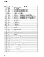
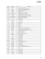

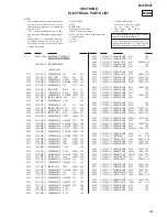
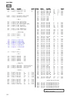
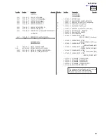


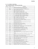

6
6
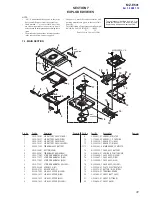
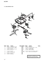
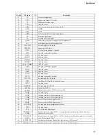
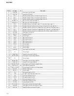
MZ-E501
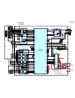
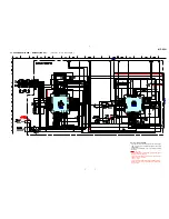
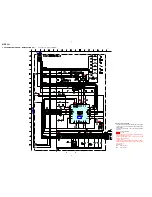
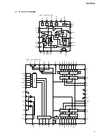
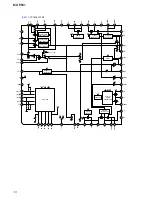
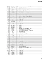
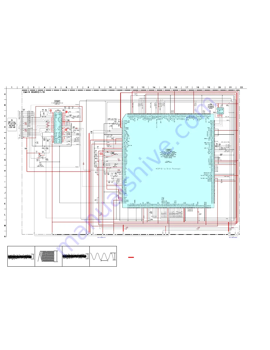
2-4. SCHEMATIC DIAGRAM – MAIN SECTION (1/3) –
Note on Schematic Diagram
• All capacitors are in
µ
F unless otherwise noted.
pF:
µµ
F 50 WV or less are not indicated except
for electrolytics and tantalums.
• All resistors are in
Ω
and
1
/
4
W or less unless
otherwise specified.
•
f
: internal component.
•
: B+ Line.
• Power voltage is dc 1.5V and fed with regulated
dc power supply from battery terminal.
• Voltages and waveforms are dc with respect to
ground under no-signal conditions.
no mark : PLAY
r
WAVEFORMS
1
2
3
4
Approx.
12 mVp-p
X601 (OSCO)
IC501
rs
(FE)
IC501
ed
(RF OUT)
IC501
1
TE
Approx.
1.2 Vp-p
Approx.
10 mVp-p
2.7 V
22.1 ns
• Voltages are taken with a VOM (Input imped-
ance 10 M
Ω
).
Voltage variations may be noted due to normal
production tolerances.
• Waveforms are taken with a oscilloscope.
Voltage variations may be noted due to normal
production tolerances.
• Circled numbers refer to waveforms.
• Signal path.
F
: Audio (Analog)
J
: Audio (Digital)
*
Replacement of IC601 used in this set requires
a special tool.
•
The voltage and waveform of CSP (chip size
package) cannot be measured, because its lead
layout is different from that of conventional IC.
• See page 11, 12 for IC Pin Function Description.
Summary of Contents for MZ-E501
Page 36: ...36 MZ E501 MEMO ...