background image

MICROFILM

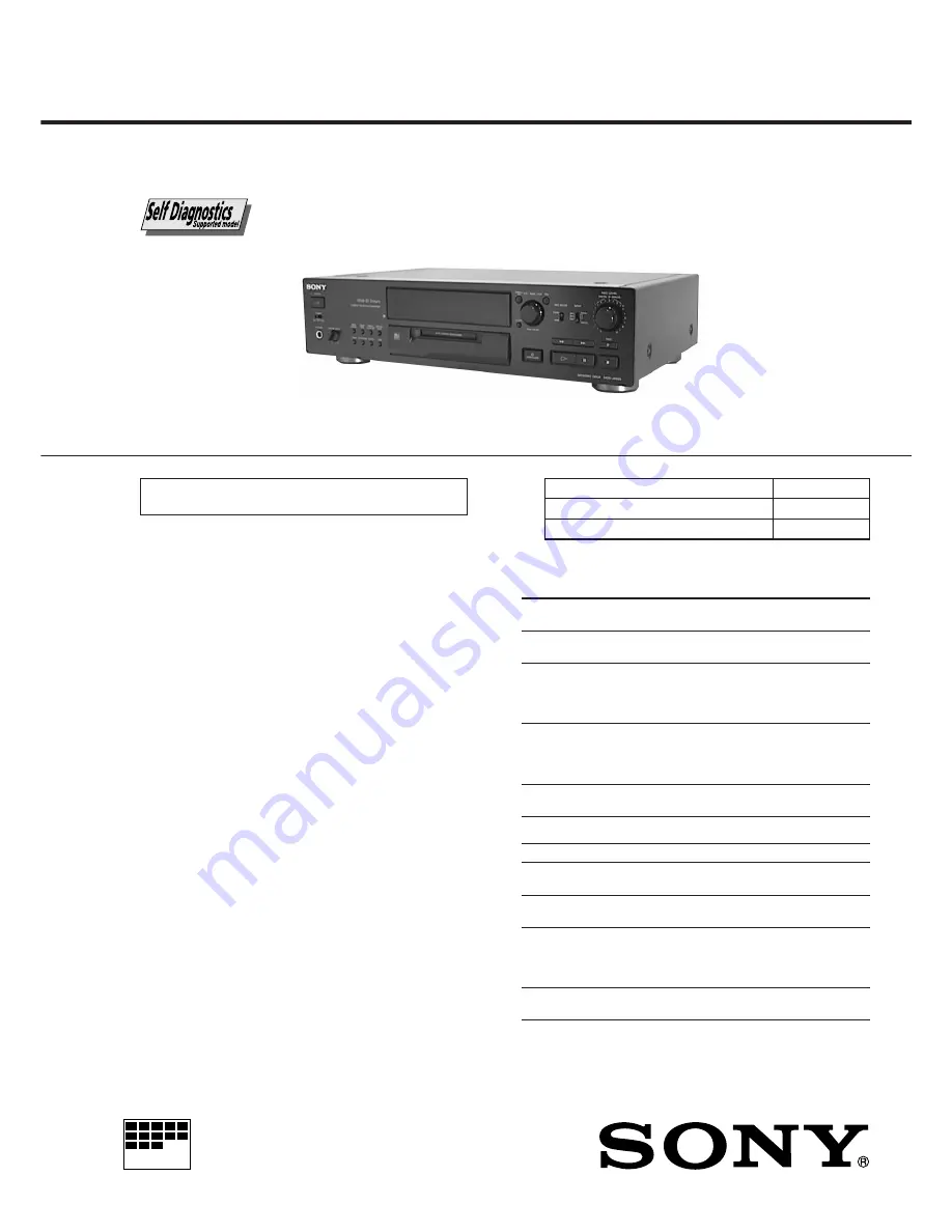
SERVICE MANUAL

MINI DISC DECK

US Model

Canadian Model

AEP Model

UK Model

SPECIFICATIONS

MDS-JB920

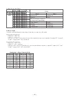
Model Name Using Similar Mechanism

MDS-JE520

MD Mechanism Type

MDM-5A

Optical Pick-up Type

KMS-260A/J1N

System

MiniDisc digital audio system

Disc

MiniDisc

Laser

Semiconductor laser (

λ

=780nm)

Emission duration: continuous

Laser output

Less than 44.6 

µ

W*

* This output is the value measured at a

distance of 200 mm from the objective lens
surface on the Optical Pick-up Block with 7
mm aperture.

Laser diode properties

Material: GaAIAs

Revolutions (CLV)

400 rpm to 900 rpm

Error correction

Advanced Cross Interleave Reed
Solomon Code (A CIRC)

Sampling frequency

44.1 kHz

Coding

Adaptive Transform Acoustic Coding
(ATRAC)

Modulation system

EFM (English-to-Fourteen Modulation)

Number fo channels

2 setero channels

Frequency response

5 to 20,000 Hz ±0.3 dB

Signal-to-noise retio

Over 100 dB during playback

Wow and flutter

Below measureble limit

U.S. and foreign patents licensed form Dolby Laboratories
Licensing Corporation.

Inputs

jack

input

Rated

Minimum

type

impedance

input

input

LINE (ANALOG) phono

47 kilohms

500 mVrms 125 mVrms

IN

jacks

DIGITAL

Square

Optical wave

OPTICAL IN1

optical

length:

       —

      —

connector

660 nm

jack

DIGITAL

Square

Optical wave

OPTICAL IN2

optical

length:

       —

      —

connector

660 nm

jack

DIGITAL

Phono

75 ohms

0.5 Vp-p

      —

COAXIAL IN

jack

±20%

Outputs

jack type

Rated output

Load impedance

PHONES

Stereo

28 mW

32 ohms

phone jack

LINE (ANALOG) Phono

2 Vrms

Over

OUT

jacks

(at 50 kilohms)

10 kilohms

DIGIRAL

Square

–18 dBm

Optical wave

OPTICAL OUT

optical

length:

connector

660 nm

jack

DIGITAL

Phono

0.5 Vp-p

75 ohms

COAXIAL OUT

jack

(at 75 ohms)

Summary of Contents for MDS-JB920

Page 1: ... Modulation system EFM English to Fourteen Modulation Number fo channels 2 setero channels Frequency response 5 to 20 000 Hz 0 3 dB Signal to noise retio Over 100 dB during playback Wow and flutter Below measureble limit U S and foreign patents licensed form Dolby Laboratories Licensing Corporation Inputs jack input Rated Minimum type impedance input input LINE ANALOG phono 47 kilohms 500 mVrms 12...

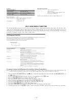
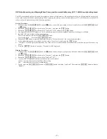
Page 2: ... Diagnosis Function Error History Display Mode Procedure for using the Self Diagnosis Function Error History Display Mode Note Perform the self diagnosis function in the error history display mode in the test mode The following describes the least required procedure Be careful not to enter other modes by mistake If you set other modes accidentally press the MENU NO button to exit the mode 1 While ...

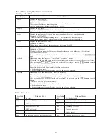
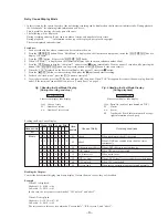
Page 3: ...s 0π E π indicates the history number The smaller the number the more recent is the error 00 is the latest indicates the error code Refer to the following table for the details The error history can be switched by rotating the AMS knob er refresh Mode which erases the retry err total err and err history histories When returning the unit to the customer after completing repairs perform this to eras...

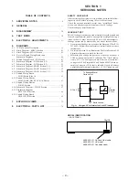
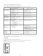
Page 4: ... of a passive VOM that is suitable Nearly all battery operated digital multimeters that have a 2 VAC range are suit able See Fig A Fig A Using an AC voltmeter to check AC leakage 1 5 kΩ 0 15 µF AC voltmeter 0 75 V To Exposed Metal Parts on Set Earth Ground MODEL IDENTIFICATION BACK PANEL Part No 4 998 603 1 π AEP and UK models 4 998 603 3 π US model 4 998 603 4 π Canadian model TABLE OF CONTENTS 1...

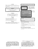
Page 5: ...e fabrikat og type Levér det brugte batteri tilbage til leverandøren CAUTION Danger of explosion if battery is incorrectly replaced Replace only with the same or equivalent type recommended by the manufacturer Discard used batteries according to the manufacturer s instruc tions CAUTION Use of controls or adjustments or performance of procedures other than those specified herein may result in hazar...

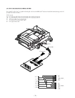
Page 6: ...I 3V For measuring IOP Check the deterioration of the optical pick up laser IOP For measuring IOP Check the deterioration of the optical pick up laser TE TRK error signal Traverse adjustment VC Reference level for checking the signal RF RF signal Check jitter CN110 RF 5P Connector 6P connector VC TEO IOP I 3V GND Mechanism deck RF VC TEO MDM 3 MDM 5 IOP I 3V VC RF TEO IOP I 3V GND VC RF TEO IOP I ...

Page 7: ...he IOP value written on the optical pick up To select the number Rotate the AMS knob To select the digit Press the AMS knob 6 When the YES button is pressed the display becomes Measu is an arbitrary number 7 As the adjustment results are recorded for the 6 value Leave it as it is and press the YES button 8 Complete will be displayed momentarily The value will be recorded in the non volatile memory...

Page 8: ...ture compensation offset check 5 6 1 See page 25 Criteria for Determination Unsatisfactory if specified value is not satisfied Clean the optical pick up Adjust again Replace the optical pick up Replace the optical pick up Replace the optical pick up Replace the optical pick up Replace the optical pick up If always unsatisfactory Replace the overwrite head Check for disconnection of the circuits ar...

Page 9: ...nect the power plug from the outlet If the test mode cannot be exited refer to Forced Reset on page 8 r Fig 1 Reading the Test Mode Display During recording and stop RTs c c Fluorescent display tube display Cause of retry Number of retries Number of retry errors Fig 2 Reading the Test Mode Display During playback Fluorescent display tube display Parts No name of area named on TOC Cluster Sector Tr...

Page 10: ...splay into binary display If more than two causes they will be added Example When 84 is displayed Higher bit 8 1000 n b7 Lower bit 4 0100 n b2 In this case as b2 and b7 are 1 and others are 0 it can be determined that the retry cause is combined of emphasis OFF monaural original copyright exists and write allowed Example When 07 is displayed Higher bit 0 1000 n All 0 Lower bit 7 0111 n b0 b1 b2 In...

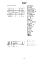
Page 11: ...S knob YES button REC MODE switch 0 button INPUT switch REC LEVEL knob ANALOG REC LEVEL knob DIGITAL ª PHONES jack º PHONE LEVEL knob FADER button PLAY MODE button REPEAT button TIME button DISC slot CLEAR button EJECT button button ª P button º p button r REC button 1 LINE ANALOG IN jacks 2 LINE ANALOG OUT jacks 3 S LINK CONTROL A1 jacks 4 DIGITAL COAXIAL IN jack 5 DIGITAL OPTICAL IN1 IN2 connect...

Page 12: ... 12 ...

Page 13: ... 13 ...

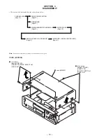
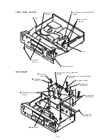
Page 14: ...er shown below CASE 4095269 Page 14 FRONT PANEL SECTION Page 15 MAIN BOARD Page 15 MECHANISM SECITON MDM 5A Page 16 BASE UNIT MBU 5A BD BOARD Page 17 SW BOARD LOADING MOTOR M103 Page 17 SLIDER CAM Page 16 1 four screws tapping SILVER CASE3 TP2 BLACK EXCEPT UK CASE UK 2 case 4095269 1 three screws tapping SILVER CASE 3 TP2 BLACK EXCEPT UK CASE UK ...

Page 15: ...wire flat type 21 core MAIN DISP CN800 1 two connectors CN801 2 wire flat type 21 core MAIN BD CN402 2 wire flat type 23 core CN400 4 MAIN board 2 wire flat type 21 core MAIN DISP CN800 1 connector CN200 1 connector CN200 3 three screws BVTP3 8 3 two screws BVTP3 8 1 two connectors CN100 801 3 seven screws BVTP3 8 ...

Page 16: ...re flat type 21 core MAIN BD CN402 2 wire flat type 23 core CN400 SLIDER CAM 1 two screws P2 6x6 2 bracket Guide L 3 leaf spring 5 bracket Guide R 6 slider Cam 4 two screws P2 6x6 Set the shaft of Lever O C to be at the position in the figure Set the shaft of Cam gear to be at the position in the figure Note for Installation of Slider A Cam ...

Page 17: ...ase unit MBU 5A 3 Remove the solder Five portion 4 screw M1 7 4 6 flexible board CN101 7 BD board 5 flexible board CN104 SW BOARD LOADING MOTOR M103 5 three screws BTP2 6 6 6 SW board 4 loading motor M103 3 two screws PWH1 7 4 1 screw PTPWH M2 6 6 2 gear B ...

Page 18: ...thods of entering the test mode Procedure 1 While pressing the AMS knob and p button connect the power plug to an outlet and release the AMS knob and p button When the test mode is set Check will be displayed Rotating the AMS knob switches between the following four groups N n Check N n Adjust N n Service N n Develop N n Procedure 2 While pressing the AMS knob connect the power plug to the outlet ...

Page 19: ... transmission Status display Error history display clear Sled check Access check Outermost circumference check Head position check Same functions as CPLAY MODE Same functions as CREC MODE Initialization of non volatile memory of adjustment value Auto gain output level adjustment MO Auto gain output level adjustment CD IOP data display IOP data write Microprocessing version display Continuous play ...

Page 20: ...the AMS knob and display CREC MODE 3 Press the YES button to change the display to CREC MID C31 4 When access completes the display changes to CREC and REC lights up Note The numbers displayed shows you the recording position addresses 2 Changing the parts to be recorded 1 When the YES button is pressed during continuous recording the display changes as below When pressed another time the parts to...

Page 21: ...ed as follows AG ππ ππππ ππ 5 Detrack check display Not used in servicing The detrack is displayed as follows ADR πππππππ 6 IVR display Not used in servicing The IVR is displayed as follows ππ ππ ππ Contents Sets continuous playback when pressed in the STOP state When pressed during continuous playback the tracking servo turns ON OFF Stops continuous playback and continuous recording The sled move...

Page 22: ...servo OFF Recording mode ON CLV low speed mode ABCD adjustment completed Tracking offset cancel ON Tracking auto gain OK Focus auto gain OK Pit High reflection CLV S CLV LOCK STOP CLV OFF Tracking servo ON Recording mode OFF CLV normal mode Tracking offset cancel OFF Groove Low reflection CLV A CLV UNLOCK MEANINGS OF OTHER DISPLAYS ...

Page 23: ...g playback check Parts Replacement and Repair NG Has the OWH been replaced NO OK NO NO NO Has OP IC171 IC101 or IC121 been replaced YES YES Initial setting of the adjustment value Has OP or IC171 been replaced YES IOP information recording IOP value labeled on OP Has IC171 or D101 been replaced YES Temperature compensation offset adjustment Laser power adjustment Traverse adjustment Focus bias adj...

Page 24: ...4 963 646 01 TEST DISK MDW 74 AU 1 Parts No 8 892 341 41 Laser power meter LPM 8001 Parts No J 2501 046 A or MD Laser power meter 8010S Parts No J 2501 145 A Oscilloscope Measure after performing CAL of prove Digital voltmeter Thermometer Jig for checking BD board waveform Parts No J 2501 149 A 5 When observing several signals on the oscilloscope etc make sure that VC and ground do not connect ins...

Page 25: ...n is effective at all times to stop the laser emission Optical pick up objective lens laser power meter BD board digital voltmeter CN110 pin 5 I 3V CN110 pin 4 IOP KMS260A 27X40 B0567 lOP 56 7 mA in this case lOP mA Digital voltmeter reading mV 1 Ω Optical pick up label Note 1 After step 4 each time the YES button is pressed the display will be switched between LD 0 7 mW LD 6 2 mW and LD Wp Nothin...

Page 26: ...R is below 2 7 Press the YES button and display b Check that the C1 error is below 220 and ADER is below 2 8 Press the YES button and display a Check that the C1 error is below 220 and ADER is below 2 9 Press the MENU NO button next press the EJECT but ton and remove the test disc 6 5 C PLAY Checking MO Error Rate Check Checking Procedure 1 Load a test disk MDW 74 AU 1 2 Rotate the AMS knob and di...

Page 27: ...er adjustment 3 To end press the AMS button or MENU NO button to display Iop Read 9 TEMPERATURE COMPENSATION OFFSET ADJUTMENT Save the temperature data at that time in the non volatile memory as 25 C reference data Note 1 Usually do not perform this adjustment 2 Perform this adjustment in an ambient temperature of 22 C to 28 C Perform it immediately after the power is turned on when the internal t...

Page 28: ...hing needs to be performed here KMS260A 27X40 B0567 lOP 56 7 mA in this case lOP mA Digital voltmeter reading mV 1 Ω Optical pick up label 11 TRAVERSE ADJUSTMENT Connection Adjusting Procedure 1 Connect an oscilloscope to CN110 pin 3 TE and CN110 pin 1 VC of the BD board 2 Load a disc any available on the market Refer to Note 1 3 Press the button and move the optical pick up outside the pit 4 Rota...

Page 29: ...orm 18 Press the YES button display EFB SAV for a mo ment and save the adjustment results in the non volatile memory Next EF CD ADJUS will be displayed 19 Press the EJECT button and remove the check disc MD TDYS 1 12 FOCUS BIAS ADJUSTMENT Adjusting Procedure 1 Load a test disk MDW 74 AU 1 2 Rotate the AMS knob and display CPLAY MODE C29 3 Press the YES button and display CPLAY MID 4 Press the MENU...

Page 30: ...below 220 and ADER is below 2 8 Press the YES button and display a Check that the C1 error is below 220 and ADER is below 2 9 Press the MENU NO button next press the EJECT but ton and remove the continuously recorded disc Note 1 If the C1 error and ADER are above other than the specified value at points a step 8 in the above or b step 7 in the above the focus bias adjustment may not have been carr...

Page 31: ...INTS AND CONNECTING POINTS BD BOARD SIDE A CN110 NOTE D101 I 3V IOP TE RF VC GND IC171 IC121 IC101 IC192 CN101 Note It is useful to use the jig for checking the waveform Refer to Servicing Notes on page 6 BD BOARD SIDE B ...

Page 32: ... circuit BPF3T 24 VCC Power supply terminal 3 3V 25 WBLADJ I Center frequency setting terminal for the internal circuit BPF22 26 TE O Tracking error signal output to the CXD2654R IC121 27 CSLED I Connected to the external capacitor for low pass filter of the sled error signal 28 SE O Sled error signal output to the CXD2654R IC121 29 ADFM O FM signal output of the ADIP 30 ADIN I Receives a ADIP FM ...

Page 33: ...2Fs 22 5792 MHz output terminal Not used open 18 XTSL I Input terminal for the system clock frequency setting L 45 1584 MHz H 22 5792 MHz fixed at H in this set 19 DIN0 I Digital audio signal input terminal when recording mode for digital optical in digital coaxial in 20 DIN1 I Digital audio signal input terminal when recording mode Not used fixed at L 21 DOUT O Digital audio signal output termina...

Page 34: ...t of the A D converter input signal Not used open 70 AVDD Power supply terminal 3 3V analog system 71 ADRT I A A D converter operational range upper limit voltage input terminal fixed at H in this set 72 ADRB I A A D converter operational range lower limit voltage input terminal fixed at L in this set 73 AVSS Ground terminal analog system 74 SE I A Sled error signal input from the CXA2523AR IC101 ...

Page 35: ...signal output to the BH6511FS IC152 94 SPFD O Spindle servo drive PWM signal output to the BH6511FS IC152 95 FGIN I S 96 TEST1 I 97 TEST2 I 98 TEST3 I 99 DVSS Ground terminal digital system 100 EFMO O EFM signal output terminal when recording mode I S stands for schmitt input I A for analog input O 3 for 3 state output and O A for analog output in the column I O Input terminal for the test fixed a...

Page 36: ...et initialize Not used D A converter section in this set 19 MODE I Writing data input terminal Not used fixed at L 20 SHIFT I Serial clock signal input terminal Not used fixed at L 21 XLATCH I Serial data latch pulse signal input terminal Not used fixed at L 22 256CK O 256Fs 11 2896 MHz clock signal output terminal Not used open 23 V35D Power supply terminal 3 3V for digital system Not used open 2...

Page 37: ...verter section digital system 46 TEST2 I Input terminal for the test fixed at L 47 TEST3 I Input terminal for the test fixed at L 48 VSS1 Ground terminal for A D converter section digital system 49 NU Not used open 50 NU Not used open 51 AVSS Ground terminal for A D converter section analog system 52 LVDD Power supply terminal 5V for A D converter section buffer system 53 LVSS Ground terminal for ...

Page 38: ...erminal L power down normally H 20 XINT I Interrupt status input from the CXD2654R IC121 21 DVOL1 I Digital rec level volume input terminal 22 DVOL0 I Digital rec level volume input terminal 23 to 30 NC I Not used fixed at L 31 SWDT O Writing data output to the CXD2654R IC121 and D A converter IC200 32 SRDT I Reading data input from the CXD2654R IC121 33 SCLK O Serial clock signal output to the CX...

Page 39: ...utput to the loading motor driver IC400 L active 1 80 LD LOW O Loading motor drive voltage control signal output for the loading motor driver IC400 H active 81 NC I Not used fixed at L 82 A1OUT O Sircs remote control signal output of the S LINK CONTROL A1 83 MUTE O Audio line muting on off control signal output terminal L line muting on 84 STB O Strobe signal output to the power supply circuit H p...

Page 40: ... 57 ASYO ASYI RFI SCTX HR901 OVER WRITE HEAD ADIP DEMODULATOR DECODER 78 ADFG SPINDLE SERVO F0CNT 94 93 SPFD SPRD SUBCODE PROCESSOR SAMPLING RATE CONVERTER DIGITAL AUDIO INTERFACE DIN0 DOUT DIGITAL SIGNAL PROCESSOR EFM ACIRC ENCODER DECODER SHOCK PROOF MEMORY CONTROLLER ATRAC ENCODER DECODER IC121 1 2 DADT INTERNAL BUS CLOCK GENERATOR XBCK LRCK FS256 OSCI OSCO CPU INTERFACE MONITOR CONTROL 10 XRST...

Page 41: ...OCK GENERATOR 1024FS CLOCK BUFFER TIMING CONTROL 5V A D CONVERTER IC100 B FOR ANALOG SECTION 5V A D D A CONVERTER IC100 200 B FOR DIGITAL SECTION SYS 3 3V 5V D A CONVERTER IC200 B FOR ANALOG SECTION 82 A1OUT 7 A1IN D A CONVERTER IC200 CURRENT PULSE IC204 2 6 29 4 41 47 43 DATA IN1 DADT BCK LRCK BCK LRCK L1 R CH BCK ATT XIN 48 64FSI 28 40 XOUT 64FSO 35 FLDATA 37 FLCLK 34 70 69 68 FLCS 2 JOG0 GND SW...

Page 42: ...ations may be noted due to normal produc tion tolerances Waveforms are taken with a oscilloscope Voltage variations may be noted due to normal produc tion tolerances Circled numbers refer to waveforms Signal path E PB j REC p PB Digital out l REC Digital in Abbreviation CND Canadian model Note The components identi fied by mark or dotted line with mark are criti cal for safety Replace only with pa...

Page 43: ...ocation Ref No Location D101 A 1 D181 D 3 D183 D 3 IC103 B 1 IC171 D 1 Q102 B 1 Q103 B 1 Q104 B 1 Semiconductor Location Ref No Location IC101 A 3 IC121 C 3 IC123 D 2 IC124 C 3 IC152 B 1 IC181 C 1 IC192 D 1 Q101 B 3 Q162 B 3 Q163 B 3 Q181 C 1 Q182 C 2 MAIN BOARD CN400 Page 64 MAIN BOARD CN402 Page 63 ...

Page 44: ...MDS JB920 49 50 6 6 SCHEMATIC DIAGRAM BD Section 1 2 See page 53 for Waveforms See page 70 and 71 for IC Block Diagrams Page 51 Page 51 Page 51 Page 52 Page 52 Page 52 Page 52 ...

Page 45: ...layback mode no mark Stop PB REC Impossible to measure The components identified by mark or dotted line with mark are critical for safety Replace only with part number specified Les composants identifiés par une marque sont critiques pour la sécurité Ne les remplacer que par une piéce portant le numéro spécifié Page 57 Page 55 Page 50 Page 49 Page 49 Page 49 Page 50 Page 50 Page 50 ...

Page 46: ...Vp p 0 06Vp p 3 2 Vp p 44 1 kHz 3 8 Vp p 2 822 MHz 3 8 Vp p 11 29 MHz 3 2 Vp p 176 4 kHz MAIN board 1 IC200 2 BCK 3 4 Vp p 350 ns 3 5 Vp p 23 µs 5 9 Vp p 45 MHz 5 IC200 º 64FSO 6 IC100 0 LRCK1 7 IC100 BCK1 8 IC800 XT OUT DISP board 1 IC771 OSCO 2 IC771 OSCI 9 IC800 XOUT 3 4 Vp p 350 ns 3 5 Vp p 32 768 kHz 3 9 Vp p Approx 2 5 MHz 0 6 Vp p Approx 2 1 MHz 3 5 Vp p 7 MHz 3 7 Vp p 23 µs 5 2 Vp p 350 ns...

Page 47: ...MDS JB920 55 56 6 8 SCHEMATIC DIAGRAM MAIN Section 1 3 See page 54 for Waveforms See page 72 and 73 for IC Block Diagrams Page 69 Page 51 Page 68 Page 59 Page 68 Page 57 ...

Page 48: ...ntified by mark or dotted line with mark are critical for safety Replace only with part number specified Les composants identifiés par une marque sont critiques pour la sécurité Ne les remplacer que par une piéce portant le numéro spécifié 6 9 SCHEMATIC DIAGRAM MAIN Section 2 3 See page 72 and 73 for IC Block Diagrams Page 51 Page 59 Page 56 ...

Page 49: ...GRAM MAIN Section 3 3 See page 53 and 54 for Waveforms See page 72 and 73 for IC Block Diagrams Note Voltages and waveforms are dc with respect to ground in playback mode no mark PB Impossible to measure Page 68 Page 68 Page 58 Page 56 ...

Page 50: ...MDS JB920 61 62 6 11 PRINTED WIRING BOARD MAIN Board side A See page 45 for Circuit Boards Location ...

Page 51: ... J 4 IC103 J 3 IC200 G 6 IC203 H 4 IC204 G 4 IC205 H 5 IC241 G 3 IC242 H 3 IC243 G 2 IC244 H 2 IC300 E 2 IC301 C 2 IC302 D 1 IC303 C 1 IC304 A 1 IC305 C 1 IC400 F 5 IC700 E 4 IC701 B 3 IC702 B 2 IC703 B 3 IC704 E 3 IC705 D 4 IC800 H 9 Q200 H 1 Q201 G 2 Q202 H 2 Q203 G 1 Q400 F 6 Q401 F 6 Q702 E 3 Q800 F 1 6 12 PRINTED WIRING BOARDS MAIN Board side B AC BAT Boards See page 45 for Circuit Boards Loc...

Page 52: ...MDS JB920 65 66 6 13 PRINTED WIRING BOARDS PANEL Section See page 45 for Circuit Boards Location US CND US CND Page 63 Page 64 Page 63 Page 64 Page 66 Page 65 ...

Page 53: ...MDS JB920 67 68 6 14 SCHEMATIC DIAGRAM PANEL Section See page 54 for Waveforms Note Voltages and waveforms are dc with respect to ground in playback mode no mark Stop Page 60 Page 56 Page 60 Page 55 ...

Page 54: ... 35 ABCD 34 FE 33 AUX 32 ADFG 31 ADAGC 30 ADIN 29 ADFM 28 SE 27 CSLED 26 TE 25 WBLADJ 24 VCC 23 3TADJ 22 EQADJ 21 VREF 20 F0CNT 19 XSTBY 18 XLAT 17 SCLK 16 SWDT 15 TEMPR 14 TEMPI 13 GND 12 APCREF 11 APC 10 PD 9 F 8 E 7 D 6 C 5 B 4 A 3 VC VI CONV BGR VREF SCRI PARA DECODE AUXSW COMMAND IVR GSW FF FBAL FF TG SEA 1 2 TG TEA WBL 3T EQ DET ADIP AGC WBL BPF22 BPFC ABCDA FEA WBL ATA CVB RFA1 1 2 1 2 GRVA...

Page 55: ...CO 16 OSCI 15 TX 14 XINT 13 RECP 12 DQSY 11 SQSY 10 XRST 9 SENS 8 SRDT 7 XLAT 6 SCLK 5 SWDT 4 MNT3 3 MNT2 2 MNT1 1 MNT0 PWM GENERATOR AUTO SEQUENCER SERVO DSP CPU I F MONITOR CONTROL SPINDLE SERVO EACH BLOCK EACH BLOCK DIGITAL AUDIO I F SAMPLING RATE CONVERTER CLOCK GENERATOR SUBCODE PROCESSOR EACH BLOCK A D CONVERTER ANALOG MUX EFM ACIRC ENCODER DECODER PLL SHOCK RESISTANT MEMORY CONTROLLER ATRAC...

Page 56: ...R2 AVDDR R1 VDD2 MODULATOR MODULATOR DECIMATION FILTER DECIMATION FILTER LOW CUT FILTER LOW CUT FILTER VOLTAGE REFERENCE I O I O ATT PLM OVER SAMP FILTER MOIZE SHAPER CPU INTERFACE ATT PLM OVER SAMP FILTER NOIZE SHAPER IC101 CXA8054M 20 VREF AINR AINR OUTR VREFR OUTR OUTR AVDD VREF AVSS AINL AINL OUTL VREFL OUTL OUTL 11 19 18 17 16 15 14 13 12 1 10 2 3 4 5 6 7 8 9 IC203 204 CXA8042AS 1 2 3 4 5 6 7...

Page 57: ...2 R2 AVSSR2 INVO BCKI DATA1 LRCKI INIT ATT SHIFT LATCH SYSM NU NU NU DVSS1 DVDD1 XVDD AVDDL2 L2 L2 AVSSL2 AVSSL1 L1 L1 AVDDL1 SYNC VSUB CKCTL MUTE XVDD S P ATT MODE ATT REGISTER D F TIMNG CIRCUIT 0 DETECT MUTE CIRCUIT 1024Fs CLOCK BUFFER Buffer Buffer Buffer Buffer PLM R2 PLM R1 Buffer Buffer Buffer Buffer PLM L1 PML L2 CLOCK GENERATOR CLOCK BUFFER IIR FIR1 OVERFLOW DETECTER OR FIR2 FIR4 FIR3 IIR ...

Page 58: ...2 11 10 9 8 1 2 3 4 5 6 7 VCC GND IC700 LA5632 1 12 DELAY CIRCUIT VREF DELAY CIRCUIT 3 3V PH5 STBY VCC ANA5 SYS3 3 B BAK AC CD1 P DOWN GND CD2 S RESET 2 3 4 5 6 7 8 9 10 11 IC400 LB1641 1 2 3 4 5 6 7 8 9 10 GND MOTOR DRIVE NOISE FILTER CLAMP FWD IN REV IN VCC 1 VCC 2 NOISE FILTER MOTOR DRIVE MOTOR DRIVE MOTOR DRIVE T S D O C P FWD REV STOP CONTROL LOGIC IC701 M5293L 2 5 5k 27k OVERCURRENT LIMITTER...

Page 59: ...11 SCREW S TIGHT PTTWH 3X6 4 1 669 992 11 AC BOARD 5 3 710 901 01 SCREW TAPPING SILVER 5 4 210 291 01 SCREW CASE 3 TP2 BLACK EXCEPT UK 5 4 999 877 01 SCREW CASE UK 6 4 997 138 01 CASE 4095269 BLACK 6 4 997 138 41 CASE 4095269 SILVER 7 4 999 839 01 SCREW BVTTWH M3 STEP 8 1 783 186 11 WIRE FLAT TYPE 21 CORE MAIN BD 9 1 783 187 11 WIRE FLAT TYPE 23 CORE 10 4 923 873 01 BRACKET CORD STOPPER 11 3 703 2...

Page 60: ...592 01 BUTTON POWER BLACK 64 4 998 592 21 BUTTON POWER SILVER 65 4 997 211 01 BUTTON MODE BLACK 65 4 997 211 21 BUTTON MODE SILVER 66 4 996 690 11 LID CARTRIDGE SILVER 66 4 996 690 21 LID CARTRIDGE BLACK 67 4 976 593 01 SPRING LID TORSION 68 4 998 593 01 BUTTON EDIT BLACK 68 4 998 593 21 BUTTON EDIT SILVER 69 1 669 997 11 VOL BOARD 70 4 998 595 01 KNOB SLIDE BLACK 70 4 998 595 21 KNOB SLIDE SILVER...

Page 61: ...213 4 933 134 01 SCREW PTPWH M2 6X6 214 4 996 224 01 SCREW 1 7X3 PWH 215 4 996 227 01 LEVER HEAD 216 4 996 229 01 SPRING HEAD LEVER TORSION 217 4 996 212 01 LEVER LIMITTER 218 4 996 213 01 SPRING LIMITTER TORSION 219 4 996 214 01 SPRING SLIDER TENSION 220 4 996 216 01 SPRING HOLDER TENSION 221 4 210 396 01 SPRING LOCK TENSION 222 X 4949 246 1 SLIDER ASSY 223 X 4949 245 1 HOLDER ASSY 224 4 996 211 ...

Page 62: ... 996 265 01 SHAFT MAIN 268 4 996 256 01 SL BASE 269 4 996 257 01 RACK SL 270 4 996 263 01 SPRING CLV TORSION 271 4 988 560 01 SCREW P 1 7X6 272 4 211 036 01 SCREW 1 7X2 5 PWH HR901 1 500 502 11 HEAD OVER WRITE M101 A 4672 475 A MOTOR ASSY SPINDLE M102 A 4672 474 A MOTOR ASSY SLED S102 1 762 148 21 SWITCH PUSH 2 KEY REFLECT DET PROTECT DET 4 BASE UNIT SECTION MBU 5A The components identified by mar...

Page 63: ...UM 10uF 20 10V C102 1 163 038 00 CERAMIC CHIP 0 1uF 25V C103 1 125 822 21 TANTALUM 10uF 20 10V C104 1 125 822 21 TANTALUM 10uF 20 10V C105 1 164 232 11 CERAMIC CHIP 0 01uF 50V C106 1 163 275 11 CERAMIC CHIP 0 001uF 5 50V C107 1 163 038 00 CERAMIC CHIP 0 1uF 25V C108 1 163 038 00 CERAMIC CHIP 0 1uF 25V C109 1 163 037 11 CERAMIC CHIP 0 022uF 10 25V C111 1 164 344 11 CERAMIC CHIP 0 068uF 10 25V C112 ...

Page 64: ...5L Q162 8 729 101 07 TRANSISTOR 2SB798 DL Q163 8 729 403 35 TRANSISTOR UN5113 Q181 8 729 018 75 TRANSISTOR 2SJ278MY Q182 8 729 017 65 TRANSISTOR 2SK1764KY RESISTOR R103 1 216 049 11 RES CHIP 1K 5 1 10W R104 1 216 073 00 METAL CHIP 10K 5 1 10W R105 1 216 065 00 RES CHIP 4 7K 5 1 10W R106 1 216 133 00 METAL CHIP 3 3M 5 1 10W R107 1 216 113 00 METAL CHIP 470K 5 1 10W R109 1 216 295 00 SHORT 0 R110 1 ...

Page 65: ... 1 784 642 11 CONNECTOR BOARD TO BOARD 11P FILTER FL781 1 517 738 11 INDICATOR TUBE FLUORESCENT IC IC761 8 749 013 91 IC GP1UC8X IC771 8 759 525 49 IC MSM9201 02GS K TRANSISTOR Q781 8 729 620 05 TRANSISTOR 2SC2603 EF Q782 8 729 620 05 TRANSISTOR 2SC2603 EF RESISTOR R702 1 249 421 11 CARBON 2 2K 5 1 4W R703 1 247 843 11 CARBON 3 3K 5 1 4W R704 1 249 425 11 CARBON 4 7K 5 1 4W R705 1 249 429 11 CARBO...

Page 66: ...00uF 20 25V C126 1 126 023 11 ELECT 100uF 20 25V C128 1 126 023 11 ELECT 100uF 20 25V C129 1 126 023 11 ELECT 100uF 20 25V C130 1 110 335 11 MYLAR 100PF 5 50V C131 1 110 335 11 MYLAR 100PF 5 50V C132 1 126 022 11 ELECT 47uF 20 25V C135 1 164 159 11 CERAMIC 0 1uF 50V C136 1 164 159 11 CERAMIC 0 1uF 50V C137 1 164 159 11 CERAMIC 0 1uF 50V C138 1 126 049 11 ELECT 22uF 20 25V C139 1 126 049 11 ELECT 2...

Page 67: ...161 494 00 CERAMIC 0 022uF 25V C703 1 164 159 11 CERAMIC 0 1uF 50V C704 1 126 927 11 ELECT 2200uF 20 10V C705 1 164 159 11 CERAMIC 0 1uF 50V C706 1 117 850 11 ELECT 15000uF 20 16V C707 1 126 964 11 ELECT 10uF 20 50V C708 1 164 159 11 CERAMIC 0 1uF 50V C709 1 126 939 11 ELECT 10000uF 20 16V C710 1 126 969 11 ELECT 220uF 20 50V C711 1 164 159 11 CERAMIC 0 1uF 50V C712 1 128 554 11 ELECT 330uF 20 63V...

Page 68: ...70 IC GP1F38R DIGITAL OPTICAL IN1 IC304 8 749 012 69 IC GP1F38T DIGITAL OPTICAL OUT IC305 8 759 242 70 IC TC7WU04F IC400 8 759 822 09 IC LB1641 IC700 8 759 525 48 IC LA5632 IC701 8 759 633 42 IC M5293L IC702 8 759 604 95 IC M5F79M07L IC703 8 759 605 00 IC M5F78M07L IC704 8 759 269 92 IC SN74HCU04ANS E20 IC705 8 759 513 71 IC PQ05RF21 IC800 8 759 526 06 IC M30610MCA 264FP IC LINK ICP703 1 532 844 2...

Page 69: ...5 1 6W R238 1 259 418 11 CARBON 390 5 1 6W R239 1 259 418 11 CARBON 390 5 1 6W R240 1 259 418 11 CARBON 390 5 1 6W R241 1 259 418 11 CARBON 390 5 1 6W R242 1 259 452 11 CARBON 10K 5 1 6W R243 1 259 452 11 CARBON 10K 5 1 6W R244 1 259 452 11 CARBON 10K 5 1 6W R245 1 259 452 11 CARBON 10K 5 1 6W R246 1 259 452 11 CARBON 10K 5 1 6W R247 1 259 452 11 CARBON 10K 5 1 6W R248 1 259 452 11 CARBON 10K 5 1 ...

Page 70: ...29 11 CARBON 10K 5 1 4W R850 1 249 429 11 CARBON 10K 5 1 4W R851 1 249 425 11 CARBON 4 7K 5 1 4W R852 1 249 393 11 CARBON 10 5 1 4W R853 1 249 426 11 CARBON 5 6K 5 1 4W R854 1 249 429 11 CARBON 10K 5 1 4W COIL T301 1 416 701 11 COIL WITH CORE VIBRATOR X200 1 579 161 11 VIBRATOR CRYSTAL 45MHz X800 1 767 778 21 VIBRATOR CERAMIC 7MHz X801 1 567 098 41 VIBRATOR CRYSTAL 32 768kHz 1 669 995 11 PSW BOARD...

Page 71: ...H 2 KEY REFLECT DET PROTECT DET T701 1 431 699 11 TRANSFORMER POWER US Canadian T701 1 431 700 11 TRANSFORMER POWER AEP UK HARDWARE LIST 1 7 685 646 79 SCREW BVTP 3X8 TYPE2 N S 2 7 685 885 09 SCREW BVTT 4X16 S 3 7 621 772 20 SCREW B 2X5 4 7 621 772 40 SCREW B 2X8 5 7 627 852 08 SCREW PRECISION P 1 7X2 5 6 7 685 533 19 SCREW BTP 2 6X6 TYPE2 N S 7 7 685 133 19 SCREW P2 6X6 TYPE2 NON SLIT ACCESSORIES...

Page 72: ... 88 MDS JB920 Sony Corporation Home A V Products Company 9 922 869 11 98E0572 1 Printed in Japan 1998 5 Published by Quality Assurance Dept Shibaura ...

Reviews: