32
MCE-SV7
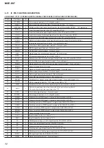
6-17.
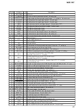
IC PIN FUNCTION DESCRIPTION
•
BD BOARD IC101 CXD3068Q (DIGITAL SIGNAL PROCESSOR, DIGITAL SERVO PROCESSOR)
Pin No.
Pin Name
I/O
Description
1
DVDD0
—
Power supply terminal (+3.3V) (digital system)
2
XRST
I
Reset signal input from the video CD controller (IC502) “L”: reset
3
MUTING
I
Muting on/off control signal input from the video CD controller (IC502) “H”: muting on
4
DATA
I
Serial data input from the video CD controller (IC502)
5
XLAT
I
Serial data latch pulse signal input from the video CD controller (IC502)
6
CLOK
I
Serial data transfer clock signal input from the video CD controller (IC502)
7
SENS
O
Internal status (SENSE) signal output to the video CD controller (IC502)
8
SCLK
I
SENSE serial data reading clock signal input from the video CD controller (IC502)
9
ATSK
I/O
Input/output terminal for anti-shock Not used (pull down)
10
WFCK
O
Write frame clock signal output terminal Not used (open)
11
XUGF
O
RFCK signal output terminal Not used (open)
12
XPCK
O
XPCK signal output terminal Not used (open)
13
GFS
O
Guard frame sync signal output terminal Not used (open)
14
C2PO
O
C2 pointer signal output to the CL680T (IC505)
15
SCOR
O
Subcode sync (S0+S1) detection signal output to the video CD controller (IC502)
16
C4M
O
4.2336 MHz clock signal output terminal Not used (open)
17
WDCK
O
Guard subcode sync (S0+S1) detection signal output terminal Not used (open)
18
DVSS0
—
Ground terminal (digital system)
19
COUT
O
Numbers of track counted signal output terminal Not used (open)
20
MIRR
O
Mirror signal output terminal Not used (open)
21
DFCT
I/O
Defect signal input/output terminal Not used (open)
22
FOK
O
Focus OK signal output terminal Not used (open)
23
PWMI
I
Spindle motor external control signal input terminal Not used (fixed at “L”)
24
LOCK
O
GFS is sampled by 460 Hz “H” output when GFS is “H”
25
MDP
O
Spindle motor (M3) servo drive signal output to the AN41020A (IC102)
26
SSTP
I
Detection signal input from limit in switch of the optical pick-up block
The optical pick-up is inner position when “H”
27
FSTO
O
2/3 divider output terminal Not used (open)
28
DVDD1
—
Power supply terminal (+3.3V) (digital system)
29
SFDR
O
Sled servo drive PWM signal (+) output to the AN41020A (IC102)
30
SRDR
O
Sled servo drive PWM signal (–) output to the AN41020A (IC102)
31
TFDR
O
Tracking servo drive PWM signal (+) output to the AN41020A (IC102)
32
TRDR
O
Tracking servo drive PWM signal (–) output to the AN41020A (IC102)
33
FFDR
O
Focus servo drive PWM signal (+) output to the AN41020A (IC102)
34
FRDR
O
Focus servo drive PWM signal (–) output to the AN41020A (IC102)
35
DVSS1
—
Ground terminal (digital system)
36
TEST
I
Input terminal for the test (fixed at “L”)
37
TES1
I
Input terminal for the test (fixed at “L”)
38
VC
I
Middle point voltage (+1.65V) input from the CXA2581N (IC103)
39
FE
I
Focus error signal input from the CXA2581N (IC103)
40
SE
I
Sled error signal input from the CXA2581N (IC103)
41
TE
I
Tracking error signal input from the CXA2581N (IC103)
42
CE
I
Middle point servo analog signal input from the CXA2581N (IC103)
43
RFDC
I
RF signal input from the CXA2581N (IC103)
44
ADIO
O
Output terminal for the test Not used (open)
Summary of Contents for MCE-SV7
Page 53: ...53 MCE SV7 MEMO ...

