background image

– 26 –

KV-PF21K70

RM-960

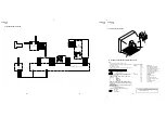
4-2. ADJUSTMENT METHOD

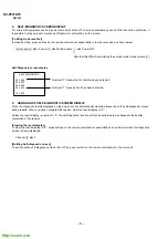
Item Number 00 of device GEO

This explanation uses H-Position as an example.

1. Select “GEO 00 HPS” with the 

1

 and 

4

 buttons.

2. Raise/lower the data with the 

3

 and 

6

 buttons.

3. Select the optimum state. (The standard is 1F for PAL reception.)

4. Write with the 

[MUTING]

 button. (The display changes to

WRITE.)

5. Execute the writing with the 

-

 button. (The WRITE

display will be changed to red color while excuting, and back

to SERVICE.)

Use the same method for all Items. Use 

1

 and 

4

 to select the

adjustment item, use 

3

 and 

6

 to adjust, write with 

[MUTING]

,

then execute the write with 

-

.

Note : 1. In 

[WRITE]

, the data for all items are written into memory

together.

2. For adjustment items that have different standard data

between 50Hz or 60Hz, be sure to use the respective

input signal after adjustment.

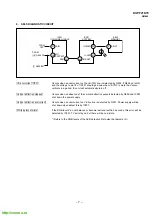
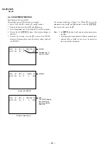
1F

SERVICE 50

HPS

Adjusted with 

[3]


and 

[6]

 buttons.

GREEN

Written with 

[MUTING]

Write executed with 

[0]

GEO

00

7F

0

000A

59

628S 1.0C

1F

SERVICE 50

HPS

RED
The WRITE display
then the display 
returns to a green
SERVICE.

GEO

00

7F

0

000A

59

628S 1.0C

1F

WRITE

50

HPS

GREEN

GEO

00

7F

0

000A

59

628S 1.0C

Summary of Contents for KV-PF21K70 Trinitron

Page 1: ...HASSIS NO CHASSIS TRINITRON COLOR TV SERVICE MANUAL BG 3S Self Diagnosis Supported model MODEL COMMANDER DEST CHASSIS NO TV 1 2 3 4 6 7 8 9 0 5 ENT JUMP SOUND MODE CH VOL FAVORITE WAKE UP SLEEP SELECT PIC MODE CABLE AUTO PROGRAM ADD ERASE MUTING MTS VIDEO TV POWER DISPLAY ...

Page 2: ...TO SAFE OPERATION ARE IDENTIFIED IN THIS MANUAL FOLLOW THESE PROCEDURES WHENEVER CRITICAL COMPONENTS ARE REPLACED OR IMPROPER OPERATION IS SUSPECTED Note Power requirements 110 220 V AC 60 Hz Power consumption W Indicated on the rear of the TV Television system M Color system NTSC3 58 Channel coverage VHF 2 to 13 UHF 14 to 13 CATV 1 to 125 Antenna 75 ohm external terminal Audio output 3W Number of...

Page 3: ...3 3 Focus Adjustment 24 3 4 G2 Screen and White Balance Adjustments 24 4 CIRCUIT ADJUSTMENTS 4 1 Adjustments with Commander 25 4 2 Adjustment Method 26 4 3 Picture Quality Adjustments 31 4 4 A Board Adjustment After IC003 Memory Replacement 31 4 5 Picture Distortion Adjustment 32 Section Title Page 5 DIAGRAMS 5 1 Block Diagram 35 5 2 Frame Schematic Diagram 38 5 3 Circuit Boards Location 40 5 4 Sc...

Page 4: ...E Micro reset No of times STANDBY TIMER lamp flashes Does not light 2 times 5 times Self diagnostic display Diagnostic result 002 000 or 002 001 255 003 001 255 004 001 255 at the same time 005 000 or 005 001 225 101 00 or 101 001 225 Probable Cause Location Power cord is not plugged in Fuse is burned out F4601 F Board H OUT Q511 is shorted A board 13V is not supplied A board IC 503 faulty A board...

Page 5: ...al deflection stopped White balance failure 5 times One flash count is not used for self diagnostic 3 STOPPINGTHE STANDBY TIMER FLASH Turn off the power switch on the TV main unit or unplug the power cord from the outlet to stop the STANDBY TIMER lamp from flashing Lamp ON 0 3 sec Lamp OFF 3 sec Lamp OFF 0 3 sec 2 times 5 times STANDBY SLEEP lamp ...

Page 6: ...results displayed on the screen are not automatically cleared always check the self diagnostic screen during repairs When you have completed the repairs clear the result display to 0 Unless the result display is cleared to 0 the self diagnostic function will not be able to detect subsequent faults after completion of the repairs Clearing the result display To clear the result display to 0 press bu...

Page 7: ...ed by Q509 and IC001 shut down the power supply Vertical deflection overcurrent Occurs when an overcurrent on V drive line is detected by Q507 Power supply will be shut down when detect this by IC001 White balance failure If the RGB levels do not balance or become low level within 5 seconds this error will be detected by IC301 TV will stay on but there will be no picture Refers to the RGB levels o...

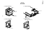
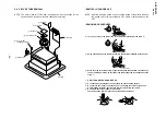
Page 8: ...SSIS ASSY REMOVAL 2 1 REAR COVER REMOVAL 2 3 F BRACKET REMOVAL 2 4 SERVICE POSITION Note Remove F Bracket first Six screws BVTP 4 16 1 2 Two screws BVTP 4 16 Rear cover 1 Chassis assy Lever Lever 1 Three connectors 2 F board Lever One screw BVTP 4 16 1 ...

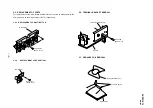
Page 9: ... and Bar Optical unscrew to exchange with the new parts and fix them with screws BVTP respectively 2 5 1 REPLACEMENT OF MULTI BUTTON 2 5 2 REPLACEMENT OF BAR OPTICAL Multi button Two screws BVTP 3 12 Bar Optical One screw BVTP 3 12 A board Terminal board bracket One screw BVTP 4 16 1 1 Demagnetization coil 2 Tension spring Picture tube ...

Page 10: ...e of anode cap A metal fitting called the shatter hook terminal is built into the rubber 3 Do not turn the foot of rubber over too hard The shatter hook terminal will stick out or damage the rubber HOW TO HANDLE AN ANODE CAP 3 When one side of the rubber cap is separated from the anode button the anode cap can be removed by turning up the rubber cap and pulling it up in the direction of the arrow ...

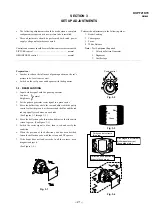
Page 11: ...ausser 3 1 BEAM LANDING 1 Input a white signal with the pattern generator Contrast Brightness 2 Set the pattern generator raster signal to a green raster 3 Move the deflection yoke to the rear and adjust with the purity control so that the green is at the center and the blue and the red take up equally sized areas on each side See Figures 3 1 through 3 3 4 Move the deflection yoke forward and adju...

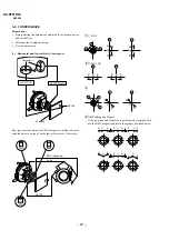
Page 12: ...tical Static Convergence Moving vertically adjust theV STAT magnet so that the red green and blue dots are on top of each other at the center of the screen 4 BMC Hexapole Magnet If the red green and blue dots are not balanced or aligned then use the BMC magnet to adjust in the manner described below 1 V STAT 2 H STAT VR 3 R G B G R B Center dot C3 board RV 702 V STAT Magnet H STAT VR BMC Hexapole ...

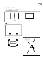
Page 13: ...Preparation Before starting this adjustment adjust the horizontal static convergence and the vertical static convergence on DY RB TLV YCH B R YCH TLV b a c d a d screen corner misconvergence a d c b a to d Permalloy assembly Fix a Permalloy assy corresponding to the misconverged areas ...

Page 14: ...te balance 7 Write into the memory by pressing MUTING then 0 3 SUB BRIGHT ADJUSTMENT 1 Set to service mode 2 Input a staircase signal of black to white from the pattern generator 3 BRIGHTNESS 50 PICTURE MINIMUM 4 Select SBR WHB7 with 1 and 4 and adjust SBR WHB7 level with 3 and 6 so that the second stripe from the right is dimly lit 3 4 G2 SCREEN AND WHITE BALANCE ADJUSTMENTS 1 G2 SCREEN ADJUSTMEN...

Page 15: ...ommander then press POWER button again hereupon it becomes TV mode c METHOD OF WRITE INTO MEMORY 1 Set to Service Mode 2 Press 1 UP and 4 DOWN select an item of adjustment 3 Press MUTING button and it will indicate WRITE on the screen 4 Press 0 button to write into memory d MEMORY WRITE CONFIRMATION METHOD 1 After adjustment pull out the plug from AC outlet and then plug into AC outlet again 2 Tur...

Page 16: ...ERVICE Use the same method for all Items Use 1 and 4 to select the adjustment item use 3 and 6 to adjust write with MUTING then execute the write with Note 1 In WRITE the data for all items are written into memory together 2 For adjustment items that have different standard data between 50Hz or 60Hz be sure to use the respective input signal after adjustment 1F SERVICE 50 HPS Adjusted with 3 and 6...

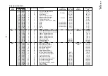
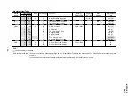
Page 17: ...Drive DYNAMIC others 0A 7 2 92 7 2 2 BDR 2A 3F B Drive DYNAMIC others 0B 7 2 93 7 2 3 RCT 7 0F R Cutoff SECAM others 07 3 0 95 3 0 4 GCT 7 0F G Cutoff SECAM others 08 7 4 96 7 4 5 BCT 7 0F B Cutoff SECAM others 08 3 0 96 3 0 6 BMN 15 1F Brightness Minimum Data 99 7 SBR 28 3F Sub Brightness Control 9A SAJ 0 PMX 33 3F Picture Maximum Data CXA2130S 88H 98 1 SHU 8 0F Sub Hue Control TV Video 9B 2 SSH ...

Page 18: ... 5 0 2 PH1 0 3 Phase 1 Register Selection 02 78 1 0 3 PH2 0 3 Phase 2 Register Selection 78 3 2 4 PH3 0 3 Phase 3 Register Selection 78 5 4 5 PH4 0 3 Phase 4 Register Selection 78 7 6 6 BCS 2 3 Base Center Shift 4 3 0 1A9 1 0 7 TCS 2 3 Treble Center Shift 5 3 0 1AA 1 0 8 TRF 2 3 RF Treble Offset 5 3 0 1AA 5 4 MSP 0 WST 15 FF W G Stereo Threshold MSP3415D 157 7 0 1 WBT EA FF W G Bilingual Threshold...

Page 19: ...Slave RAM Address Name No Name Different Data No bit Address bit 17 ERR 50 FF Auto FM switch Threshold 21 10 3 166 7 0 18 VOL 6D FF Loud Speaker gain 7000h to 7ff0h 0000 15 4 1A8 7 0 TXT 0 TXH 1 3 Teletext Horizontal Position 58 H 18D 6 4 1 TXV 0 3 Teletext Vertical Position 18D 1 0 OPM 0 OSH 0A 3F OSD H Position Option Misc B1 7 2 1 COM 0 03 Comb Selection AE 7 6 2 APC 1 1 APC Switch AD 5 3 TSY 0...

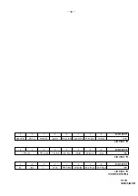
Page 20: ... SECAM 0 XTAL 3 58 1 XTAL 4 43 0 ITEM INFORMATION No OPB0 OP1 No OPB2 OP3 Color SW 1 11 KEY 0 AV Mono 1 US ST 0 Auto TV sys 0 Auto PIC 1 2199 Curve 1 Pic Rot 0 Item KV PF21K70 AV Input No OPB1 OP2 0 1 DVD Input 0 Dis Fav 0 Thai Bil 0 HDEV 0 NICAM 0 TOP 0 Item KV PF21K70 ...

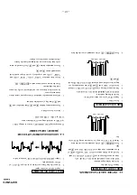
Page 21: ... the data BELL FILTER ADJUSTMENT 1 Input SECAM color bar signal 2 Connect the dual trace oscilloscope to the pin 9 R Y of CN303 not mounted 3 Adjust SERVICE MODE ITEMS SBF as shown below 4 4 A BOARD ADJUSTMENT AFTER IC003 MEMORY REPLACEMENT When replacing IC003 MEMORY be sure to change IC001 µ COM to the following new IC at the same time IC001 µ COM CXP86461 628S 1 Enter to Service Mode 2 Press co...

Page 22: ... 00 0B GEO 0 HPS H POSITION GEO 1 HSZ H SIZE GEO 2 PAP PIN AMP GEO 5 VSZ V SIZE GEO 7 VLN V LINEARITY GEO 4 VPS V POSITION GEO 6 SCO VERTICAL S Correction GEO 8 BOW AFC BOW GEO 9 AGL AFC ANGLE GEO 3 TLT TRAPEZIUM GEO 0A UCP UPPER CORNER PIN GEO 0B LCP LOWER CORNER PIN ...

Page 23: ... A51LPT70X NECK ASSY DY Y21RSA S B out R out V out U out Y out V in U in Y in VM out G out B out 22 23 24 21 19 18 11 13 14 IK in H DRIVE H PULSE E W VD VD VM DRIVE Q5902 5906 H OUT Q511 2SC4927 V OUT IC503 TDA8172 HDT T501 H DRIVE Q506 2SC2688 PIN CONT IC502 NJM2903D PIN OUT Q505 IRF614 PMC L509 HLC L510 FBT T503 NX 1748 B Audio Front Vcc audio 3D Vcc audio 3D Vcc This is not used for these model...

Page 24: ...ll voltages are in V Cannot be measured Circled numbers are waveform references B bus B bus signal path Note The component identified by shading and mark are critical for safety Replace only with part number specified Ref erence inf ormation RESISTOR RN METAL FILM RC SOLID FPRD NONFLAMMABLE CARBON FUSE NONFLAMMABLE FUSIBLE RS NONFLAMMABLE METAL OXIDE RB NONFLAMMABLE CEMENT RW NONFLAMMABLE WIREWOUN...

Page 25: ... CHIP 220 CHIP 22k CHIP 3 3k CHIP 1 5k CHIP 10k CHIP 1k CHIP 10k CHIP 330 75 CHIP 220 CHIP 470k CHIP 15k CHIP 5 6k CHIP 470 CHIP 1k CHIP 1 8k CHIP 3 3k CHIP 47 CHIP 470 CHIP 470 CHIP 100p CH CHIP 220p CH CHIP 470k CHIP 220 CHIP 75 CHIP 470k CHIP 15k CHIP 470k CHIP 68 CHIP 470 CHIP 1k CHIP 1 16V F CHIP 4 7 470p CH CHIP 470 16V 470p B CHIP 1 16V F CHIP UN2216 LSP MUTE 0 01 F CHIP 10k CHIP 100 CHIP 1...

Page 26: ...0V B 2 2k CHIP 15k 3W RS 22 2W RS ERC04 06SE ERC04 06SE TDA8172 V OUT GP08DPKG23 H POSI GP08DPKG23 H POSI 2P VH 0 0047 500V E 0 0047 500V E 0 0047 500V E 0 0047 500V E 2 2k CHIP 4 7k 1W RS 4 7k 1W RS JW 5MM 0 CHIP 0 CHIP 22k CHIP 0 47 1 2W FPRD 0 47 1 2W FPRD 0 47 1 2W FPRD GP08DPKG23 V BOOST 8 2M 1W 2P MINI 470p CH CHIP 470p CH CHIP 100 0 1 25V F CHIP 56k 0 22 2W RS 2200 25V JW 5MM SW LB HDT HDT ...

Page 27: ... 7 D605 G 10 D606 E 11 D607 F 10 D608 E 11 D609 H 8 D610 J 8 D611 I 7 D612 F 8 D613 I 7 D614 H 7 D615 E 7 D616 E 9 D617 F 8 D618 F 9 D620 D 8 D621 F 8 D622 F 7 D623 F 12 D624 F 12 D625 D 12 D627 F 8 D628 G 5 D629 F 9 D630 E 9 D631 G 12 D632 F 12 D633 E 12 D634 F 11 D635 F 12 D636 D 12 D637 F 11 D638 E 11 D901 C 13 D902 D 13 D903 C 13 D904 D 13 D905 F 13 D906 I 13 PRINTED WIRING BOARD A POWER SUPPL...

Page 28: ...4 HV KB 1 1 1 1 1 2 3 4 5 6 5 10 9 8 7 6 4 3 1 11 13 G4 G2 G1 1 H1 H2 G1 2 KB KG KR G1 3 RCV 1 2 3 R738 R739 R740 C709 C710 C704 C701 R734 R703 L701 D702 R760 R761 R762 C736 C737 C746 C703 CN705 C702 C714 L706 R723 C716 CN701 RV702 J701 CN706 D708 CN704 R705 R711 R713 R715 R712 R714 R720 R722 R724 R721 R719 R725 R726 R727 R728 R729 R730 C712 C713 R755 R756 R757 C717 R707 C706 C708 R706 D715 D714 D...

Page 29: ...0Vp p H 90Vp p H VM1 Board C3 Board PRINTED WIRING BOARD C3 BOARD WAVEFORMS C3 BOARD IC701 STV 5112S 55 56 BLUE CATHODE CURRENT RED CATHODE CURRENT GREEN CATHODE CURRENT VDD VDD BLUE INPUT GREEN INPUT RED INPUT RED FEEDBACK GREEN FEEDBACK BLUE FEEDBACK RED OUTPUT GREEN OUTPUT BLUE OUTPUT GROUND GND REFERENCE VOLTAGE VM1 VELOCITY MODULATION C3 RGB OUT ...

Page 30: ... 58 Schematic diagram F board F CISPR 1 2 1 2 1 2 3 4 1 2 3 4 CN4603 CN4601 CN4602 T4601 C654 F4601 C4601 T4602 R4601 VDR461 JW4603 JW4604 JW4601 JW4602 C4602 1P TAB 2P VH 2P VH T L F 0 0047 250V E T3 15A FUSE 250V 1M 1 2W ERZV14D621 0 47 250V PT AC IN AC IN AC OUT AC OUT GND TO A BOARD CN104 TO A BOARD CN601 CISPR B SSS10465 K F PF21 ...

Page 31: ...1EQS04 11ES2 NTA2B DTZ TT11 15B DTZ10B MA 111 K8 S0 UDZS TE17 5 1B UDZS TE17 6 8B UDZS TE17 9 1B 1SS355TE 17 5P6M DA204K SPB 26MVWF CATHODE ANODE CATHODE ANODE GRN ANODE GRN UN2111 UN2211 UN2213 UN2216 2SD2114K 2SC1162 G 2SC2712 YG 2SA1175 HFE 2SC2785 HFE 2SA1091 0 2SD2144S UVW 2SC2458 YGR 2SC2611 NJM78M09FA TA7805S E LETTER SIDE C B CXA2139S 48PIN CXP86449 628S 64PIN TDA7429L 8PIN M24C08 BN6 8PIN...

Page 32: ... 4 067 167 31 BRACKET TERMINAL 25 A 1342 453 A VM1 BOARD COMPLETE 26 4 074 017 01 BLOTTING SHEET 27 A 1241 355 A F BOARD MOUNTED 28 4 071 023 31 HOLDER HV CABLE 29 4 070 300 01 COVER REAR 30 4 064 883 03 HOLDER DGC 31 4 379 189 11 CUSHION SPEAKER 32 4 069 652 02 CUSHION HS BAND 33 4 070 292 01 BAR OPTICAL 34 8 453 011 31 NA299 S2 SECTION 6 EXPLODED VIEW NOTE Items with no part number and no descri...

Page 33: ... 470PF 10 00 50V C110 1 163 005 11 CERAMIC CHIP 470PF 10 00 50V C111 1 163 005 11 CERAMIC CHIP 470PF 10 00 50V C112 1 104 664 11 ELECT 47UF 20 00 16V C113 1 104 664 11 ELECT 47UF 20 00 25V C114 1 126 967 11 ELECT 47UF 20 00 50V C202 1 163 021 91 CERAMIC CHIP 0 01UF 10 00 50V C204 1 130 481 00 MYLAR 0 0068UF 5 00 50V C206 1 164 182 11 CERAMIC CHIP 0 0033UF 10 00 50V C209 1 126 964 11 ELECT 10UF 20 ...

Page 34: ...CERAMIC 470PF 10 00 2KV C530 1 137 372 11 MYLAR 0 022UF 5 00 50V C531 1 126 961 11 ELECT 2 2UF 20 00 50V C532 1 126 941 11 ELECT 470UF 20 00 25V C533 1 126 941 11 ELECT 470UF 20 00 25V C536 1 136 165 00 MYLAR 0 1UF 5 00 50V C537 1 126 969 11 ELECT 220UF 20 00 50V C538 1 117 657 11 FILM 8500PF 3 00 1 2KV C539 1 129 746 91 FILM 0 039UF 5 00 400V C540 1 136 171 00 MYLAR 0 33UF 5 00 50V C546 1 165 319...

Page 35: ... 61 DIODE 1SS355TE 17 D307 8 719 988 61 DIODE 1SS355TE 17 D308 8 719 988 61 DIODE 1SS355TE 17 D309 8 719 069 54 DIODE UDZS TE17 5 1B D311 8 719 988 61 DIODE 1SS355TE 17 D312 8 719 988 61 DIODE 1SS355TE 17 D313 8 719 988 61 DIODE 1SS355TE 17 D314 8 719 988 61 DIODE 1SS355TE 17 D315 8 719 988 61 DIODE 1SS355TE 17 D316 8 719 069 57 DIODE UDZS TE17 6 8B D319 8 719 069 60 DIODE UDZS TE17 9 1B D319 8 71...

Page 36: ...216 295 91 SHORT 0 JR002 1 216 295 91 SHORT 0 JR003 1 216 295 91 SHORT 0 JR004 1 216 295 91 SHORT 0 JR005 1 216 295 91 SHORT 0 JR006 1 216 295 91 SHORT 0 JR007 1 216 295 91 SHORT 0 JR008 1 216 295 91 SHORT 0 JR009 1 216 295 91 SHORT 0 JR010 1 216 295 91 SHORT 0 JR011 1 216 295 91 SHORT 0 JR012 1 216 295 91 SHORT 0 JR013 1 216 295 91 SHORT 0 JR014 1 216 295 91 SHORT 0 JR015 1 216 295 91 SHORT 0 JR0...

Page 37: ...IP 4 7K 5 1 10W R011 1 216 065 91 RES CHIP 4 7K 5 1 10W R012 1 216 065 91 RES CHIP 4 7K 5 1 10W R013 1 216 065 91 RES CHIP 4 7K 5 1 10W R014 1 216 025 91 RES CHIP 100 5 1 10W R015 1 216 025 91 RES CHIP 100 5 1 10W R017 1 216 049 91 RES CHIP 1K 5 1 10W R018 1 216 033 00 RES CHIP 220 5 1 10W R019 1 216 073 00 RES CHIP 10K 5 1 10W R021 1 216 073 00 RES CHIP 10K 5 1 10W R022 1 216 033 00 RES CHIP 220 ...

Page 38: ...558 1 249 421 11 CARBON 2 2K 5 1 4W R559 1 249 429 11 CARBON 10K 5 1 4W R560 1 216 073 00 RES CHIP 10K 5 1 10W R562 1 249 401 11 CARBON 47 5 1 4W R565 1 216 073 00 RES CHIP 10K 5 1 10W R567 1 216 105 91 RES CHIP 220K 5 1 10W R226 1 216 033 00 RES CHIP 220 5 1 10W R227 1 216 033 00 RES CHIP 220 5 1 10W R229 1 216 073 00 RES CHIP 10K 5 1 10W R230 1 216 065 91 RES CHIP 4 7K 5 1 10W R231 1 216 295 91 ...

Page 39: ... R632 1 202 933 61 FUSIBLE 0 1 10 1 2W R633 1 216 073 00 RES CHIP 10K 5 1 10W R634 1 218 265 11 METAL 8 2M 5 1W R635 1 216 492 11 METAL OXIDE 82K 5 3W R636 1 215 924 00 METAL OXIDE 15K 5 3W R637 1 216 492 11 METAL OXIDE 82K 5 3W R639 1 216 363 00 METAL OXIDE 0 33 5 2W R640 1 249 415 11 CARBON 680 5 1 4W R641 1 216 362 11 METAL OXIDE 0 27 5 2W R642 1 249 419 11 CARBON 1 5K 5 1 4W R643 1 247 843 11 ...

Page 40: ...IODE 1SS119 25TD D716 8 719 911 19 DIODE 1SS119 25TD D717 8 719 929 15 DIODE RD9 1ES T1B JACK J701 1 540 071 22 SOCKET CRT COIL L701 1 410 667 31 INDUCTOR 22UH L710 1 408 613 31 INDUCTOR 68UH L711 1 408 613 31 INDUCTOR 68UH L712 1 408 613 31 INDUCTOR 68UH TRANSISTOR Q704 8 729 326 11 TRANSISTOR 2SC3271F N Q705 8 729 326 11 TRANSISTOR 2SC3271F N Q706 8 729 326 11 TRANSISTOR 2SC3271F N Q707 8 729 20...

Page 41: ...00 50V C5914 1 126 933 11 ELECT 100UF 20 00 16V C5916 1 130 491 00 MYLAR 0 047UF 5 00 50V C5917 1 126 925 11 ELECT 470UF 20 00 10V C5918 1 115 341 51 CERAMIC 120PF 10 00 500V C5920 1 126 964 11 ELECT 10UF 20 00 50V C5921 1 101 888 00 CERAMIC 68PF 5 00 50V CONNECTOR CN5901 1 564 510 11 PLUG CONNECTOR 7P CN5904 1 770 723 11 CONNECTOR BOARD TO BOARD 8P DIODE D5901 8 719 911 19 DIODE 1SS119 25TD D5902...

Page 42: ... 4W R5932 1 249 413 11 CARBON 470 5 1 4W R5933 1 249 413 11 CARBON 470 5 1 4W R5934 1 249 430 11 CARBON 12K 5 1 4W R5935 1 249 429 11 CARBON 10K 5 1 4W MISCELLANEOUS 1 419 479 21 COIL DEGAUSSING 1 452 032 00 MAGNET DISC 1 505 547 21 SPEAKER 5X9CM 1 573 657 21 PLUG F PIN 1 775 468 31 CORD POWER WITH CONNECTOR 2 5A 250V 8 738 809 05 PICTURE TUBE A51LPT70X 8 451 505 11 DEFLECTION YOKE Y21RSA S 8 453 ...

Reviews: