background image

— 3 —

SECTION 2

DISASSEMBLY

Note :

Follow the disassembly procedure in the numerical order given.

 The equipment can be removed using the following procedure.

Key board

Cabinet (upper) 

Set

Main board

Power board

2-1.

CABINET (UPPER)

2

 Cabinet (upper)

4

 Speaker

3

Remove the two solderings.

1

1

 Five screws (M3


×

 14)

Summary of Contents for ICF-C253

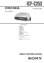
Page 1: ...ICF C253 Australian Model SERVICE MANUAL FM AM PLL SYNTHESIZED CLOCK RADIO SPECIFICATIONS Ver 1 0 2000 04 ...

Page 2: ...omer and recommend their replacement 4 Look for parts which through functioning show obvious signs of deterioration Point them out to the customer and recommend their replacement 5 Check the B voltage to see it is at the values specified 6 Flexible Circuit Board Repairing Keep the temperature of the soldering iron around 270 C during repairing Do not touch the soldering iron on the same conductor ...

Page 3: ...embly procedure in the numerical order given The equipment can be removed using the following procedure Key board Cabinet upper Set Main board Power board 2 1 CABINET UPPER 2 Cabinet upper 4 Speaker 3 Remove the two solderings 1 1 Five screws M3 14 ...

Page 4: ...2 Two claws 6 Chassis 4Key board 3Remove the eight solderings 7Cabinet lower 2 3 MAIN BOARD 8Main board 6LED board 3Alarm dial board 4Claw 7Remove the four solderings 5Remove the four solderings 1Remove the five solderings 2 Two screws BTP 2 8 ...

Page 5: ... on level meter T1 450 kHz Adjusting Location MAIN board Component Side FM RF signal generator 22 5 kHz frequency deviation by 400 Hz signal FM lead wire antenna terminal speaker terminal 0 01 µF set level meter AM RF SSG Put the lead wire antenna close to the set 30 amplitude modulation by 400 Hz signal Output level as low as possible set speaker terminal level meter 2 4 POWER BOARD 7Power board ...

Page 6: ... D6 D7 D8 D9 D10 Q151 W200 W151 E E E E 1 14 15 28 29 42 43 56 LCD100 LIQUID CRYSTAL DISPLAY E CN150 1 3 CN2 1 3 W2 1 4 W150 CN201 E E HI LOW S1 BRIGHTNESS H L 1 8 CN200 B A ALARM MODE T150 POWER TRANSFORMER P150 AC IN S213 CLOCK S210 DST S209 M5 S208 M4 S204 ON S202 OFF S207 M3 S206 M2 S205 M1 S200 S201 S203 BAND S211 SNOOZE S212 A RESET S214 S215 SP1 SPEAKER 1 2 A B C D E F 3 4 5 6 7 8 9 10 TO A...

Page 7: ...nal component C panel designation U B Line H adjustment for repair Voltages are dc with respect to ground under no signal detuned conditions no mark FM AM Impossible to measure Voltages are taken with a VOM Input impedance 10 MΩ Voltage variations may be noted due to normal produc tion tolerances Signal path F FM f AM The components identified by mark 0 or dotted line with mark 0 are critical for ...

Page 8: ... O O O O O O I I Ι O I I O I O O O I I O O I Description Initialization output Mute output Band output ALARM A indicator ALARM B indicator Key strove signal Key return signal ALARM TIME input DIAL signal Ground PLL error output LW MW VCO input FM VCO input Regulator VDD System clock output System clock input Regulator LCD bubbler LCD drive Common signal LCD drive Segment signal Not used Power fail...

Page 9: ...F 5 50V C4 1 163 141 00 CERAMIC CHIP 0 001uF 5 50V C5 1 163 021 91 CERAMIC CHIP 0 01uF 10 50V C6 1 163 227 11 CERAMIC CHIP 10PF 0 50PF 50V C7 1 163 141 00 CERAMIC CHIP 0 001uF 5 50V C8 1 126 964 11 ELECT 10uF 20 50V C9 1 126 963 11 ELECT 4 7uF 20 50V C10 1 126 964 11 ELECT 10uF 20 50V C11 1 163 085 00 CERAMIC CHIP 2PF 50V C13 1 163 021 91 CERAMIC CHIP 0 01uF 10 50V C14 1 163 809 11 CERAMIC CHIP 0 ...

Page 10: ... SHORT 0 JC6 1 216 295 91 SHORT 0 JC8 1 216 296 91 SHORT 0 JC9 1 216 296 91 SHORT 0 JC10 1 216 295 91 SHORT 0 JC12 1 216 296 91 SHORT 0 JC14 1 216 296 91 SHORT 0 JC15 1 216 296 91 SHORT 0 JC16 1 216 296 91 SHORT 0 JC17 1 216 296 91 SHORT 0 JC18 1 216 296 91 SHORT 0 JC19 1 216 296 91 SHORT 0 JC20 1 216 296 91 SHORT 0 JC21 1 216 296 91 SHORT 0 JC22 1 216 296 91 SHORT 0 JC23 1 216 295 91 SHORT 0 JC24...

Page 11: ... 2K 5 1 8W R102 1 216 089 91 RES CHIP 47K 5 1 10W R103 1 216 089 91 RES CHIP 47K 5 1 10W R104 1 216 097 91 RES CHIP 100K 5 1 10W R105 1 216 097 91 RES CHIP 100K 5 1 10W R106 1 216 065 91 RES CHIP 4 7K 5 1 10W R107 1 216 065 91 RES CHIP 4 7K 5 1 10W R108 1 216 065 91 RES CHIP 4 7K 5 1 10W R109 1 216 065 91 RES CHIP 4 7K 5 1 10W R110 1 216 073 00 METAL CHIP 10K 5 1 10W R111 1 216 001 00 METAL CHIP 1...

Page 12: ...ICF C253 16 Sony Corporation Audio Entertainment Group 2000D16053 1 Printed in Japan 2000 4 Published by PE General Engineering Dept 9 927 909 11 ...

Reviews: