background image

ICD-B17

10

10

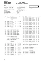
• Waveforms

1

IC101 

ta

 (XOUT)

0.5V/div   0.1µsec/div

3.98MHz

2

IC704 

1

 (32KOUT)

1.0V/div   10µsec/div

32.768kHz

3

IC704 

8

 (OSCOUT)

0.5V/div   10µsec/div

4

IC703 

ul

 (X2)

1.0V/div   0.2µsec/div

32.768kHz

5MHz

1.0Vp-p

2.2Vp-p

1.2Vp-p

3.2Vp-p

THIS NOTE IS COMMON FOR PRINTED WIRING
BOARDS AND SCHEMATIC DIAGRAMS.
(In addition to this, the necessary note is
printed in each block.)

Common Note on Schematic Diagrams:
• All capacitors are in µF unless otherwise noted.  pF: µµF

50 WV or less are not indicated except for electrolytics
and tantalums.

• All resistors are in 

 and 

1

/

4


W or less unless otherwise

specified.

f

: internal component.

C

: panel designation.

A

: B+ Line.

• Power voltage is dc 3V and fed with regulated dc power

supply from battery terminal.

• Voltage and waveforms are dc with respect to ground

under no-signal (detuned) conditions.
no mark : PB
(

) : REC

• Voltages are taken with a VOM (Input impedance 10 M

).

Voltage variations may be noted due to normal produc-
tion tolerances.

• Waveforms are taken with a oscilloscope.

Voltage variations may be noted due to normal produc-
tion tolerances.

• Circled numbers refer to waveforms.

• Signal path.

E

: PB

a

: REC

Common Note on Printed Wiring Boards:

X

: parts extracted from the component side.

Y

: parts extracted from the conductor side.

f

: internal component.

z

: Through hole.

: Pattern from the side which enables seeing.

Lead layout of conventional IC

Caution:
Pattern face side:

Parts on the pattern face side seen from

(SIDE B)

the pattern face are indicated.

Parts face side:

Parts on the parts face side seen from

(SIDE A)

the parts face are indicated.

Lead Layouts

Summary of Contents for ICD-B17 - Ic Recorder

Page 1: ... minijack monaural Plug in power Minimum input level 0 6 mV 3 kilohms or lower impedance microphone Power requirements Two LR03 sizeAAA alkaline batteries 3V DC Dimensions w h d not incl projecting parts and controls 44 5 105 3 14 0 mm 1 13 16 4 1 4 9 16 in Mass incl batteries 68 g 2 4 oz Design and specifications are subject to change without notice SPECIFICATIONS Ver 1 0 2003 05 Sony Corporation...

Page 2: ...ted with the lead free mark LF indicating the solder contains no lead Caution Some printed circuit boards may not come printed with the lead free mark due to their particular size LEAD FREE MARK Unleaded solder has the following characteristics Unleaded solder melts at a temperature about 40 C higher than ordinary solder Ordinary soldering irons can be used but the iron tip has to be applied to th...

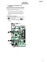
Page 3: ...n of this check is stored in the TOC AREA so that the BAD BLOCK area should not be used BAD BLOCK Check Procedure 1 When the power is turned on after the flash memory IC701 is replaced the BAD BLOCK check starts automatically and the OPR D701 lights in orange 2 In about 30 seconds after start of the check the OPR D701 changes the color to green indicating that the check is completed TP701 TP702 TP...

Page 4: ...4 ICD B17 SECTION 2 GENERAL This section is extracted from instruction manual ...

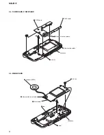
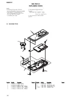
Page 5: ...ISASSEMBLY Note Follow the disassembly procedure in the numerical order given 3 1 UPPER LID ASSY 3 1 UPPER LID ASSY Page 5 3 2 F SW BOARD P SW BOARD Page 6 SET 3 3 MAIN BOARD Page 6 1 B 1 7x10 4 claw 2 B 1 7x7 7 screws 1 7x2 5 8 speaker SP101 3 claws 5 claws 9 upper lid assy case assy 6 claw ...

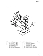
Page 6: ...SW BOARD P SW BOARD 3 3 MAIN BOARD 2 CN701 3 case assy 5 F SW board 6 P SW board 4 Removal the five solders 1 Removal the solder 4 claw 5 claw case assy 1 Removal the two solders 6 MAIN board 2 speaker SP101 3 B 1 7x4 ...

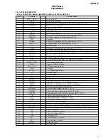
Page 7: ... output 27 BIAS O Connect to VDD LCD bias 28 30 VLC0 VLC2 LCD drive power supply pin 31 VSS0 Ground pin 32 61 S0 S29 O LCD segment signal output 62 NC I Not used Open 63 NC O Not used Open 64 XTEST I Test pin 65 DSPPOW O Digital signal processor registor control I F enable signal output 66 LEDREC O OPR REC LED D701 red ON OFF signal output 67 LEDPB O OPR PLAY LED D701 green ON OFF signal output 68...

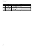
Page 8: ...lock 2 Hz signal input 88 FLMPOW O Flash memory power ON OFF signal output 89 DSPIFACK I I F acknowledge signal input to the DSP IC IC101 90 LMUTE O Line mute ON OFF signal output 91 98 FMI01 FMI07 I O Data bus signal input output 99 AVSS Ground pin 100 BATT I Power supply voltage detection signal input ...

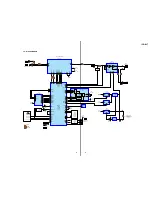
Page 9: ...ROL OSC INTERRUPT CONTROL RTCCE RTCINT RTCDI RTCCLK RTCDO AMPPOW BEEP LMUTE XT1 DSPPOW FLMPOW XRESET X1 X2 LEDPB LEDREC COM0 I COM3 S0 I S29 SI SO SCLK CE INTB 32KOUT 4 3 2 7 6 1 3 3V VCC C D701 OPR GRN PLAY RED REC A D D A CONVERTER DSP IC101 PLUG IN POWER X101 3 98MHz X701 5MHz MEMORY CONTROL SYSTEM CONTROL IC703 S706 708 713 S710 712 714 S704 705 709 715 KEY IN DETECT Q703 705 VCC 3 3V VCCB VCC...

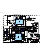
Page 10: ...th regulated dc power supply from battery terminal Voltage and waveforms are dc with respect to ground under no signal detuned conditions no mark PB REC Voltages are taken with a VOM Input impedance 10 MΩ Voltage variations may be noted due to normal produc tion tolerances Waveforms are taken with a oscilloscope Voltage variations may be noted due to normal produc tion tolerances Circled numbers r...

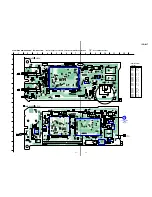
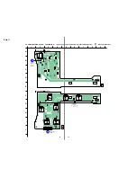
Page 11: ... R704 C701 R119 C132 C704 R702 R729 Q702 Q703 Q704 C711 R707 C706 R711 R101 R712 R713 C123 R120 C124 C125 R710 C730 R706 C705 C728 R758 R760 R756 R116 RED REC D701 OPR GRN PLAY Q701 C C B B E E B C C E B C104 C119 C121 C131 C702 IC103 C504 C103 C714 C502 C510 C703 C707 C509 C505 X101 J102 EAR J101 MIC PLUG IN POWER X701 E B C B C E IC702 1 2 3 E B C Q705 B E C IC505 IC506 4 D S G 5 3 2 1 2 1 3 IC5...

Page 12: ... 9 R744 CN501 10 6 5 1 R747 TP744 TP749 TP748 TP747 TP743 TP741 TP742 R745 R746 R742 R753 R743 11 11 1 688 236 F SW BOARD SIDE A F SW BOARD SIDE B 11 11 1 688 236 DRY BATTERY SIZE AAA IEC DESIGNATION LR03 2PCS 3V S704 MENU W703 W704 W702 W701 W706 P SW BOARD B S708 STOP S709 z ERASE S707 DISPLAY S715 MIC SENS S706 INDEX S705 FOLDER MAIN BOARD CN701 A Page 13 Page 11 ...

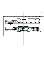
Page 13: ...37 F SW BOARD B 0FF ON R750 R751 R749 R748 R752 S712 S713 X PAUSE S711 z REC STOP S703 HOLD S714 SELECT S710 B x P SW BOARD SIDE A P SW BOARD SIDE B W713 W714 W712 W711 W716 PUSH PLAY STOP ENTER B 4 5 PRINTED WIRING BOARD P SW SECTION Refer to page 10 for Common Note on Printed Wiring Boards Uses unleaded solder Page 12 ...

Page 14: ...504 IC503 IC502 C127 R130 R131 R132 R133 R134 R129 R128 R127 R126 R125 R124 R123 R121 R122 C126 C107 R116 C128 R135 C129 C131 C119 C120 FB102 FB101 R117 C121 R119 R120 C123 IC103 J102 FB103 TP106 FB104 TP105 TP104 C730 TP502 TP107 TP501 TP503 TP504 L501 TP506 TP505 TP507 TP508 C504 C510 C502 CN701 CN501 R746 R747 R743 R753 R744 R745 R742 S705 S704 S715 S709 S708 S707 S706 W704 W701 W702 W703 W706 ...

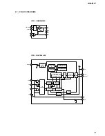
Page 15: ... REGISTER I O CONTROL ADDRESS DECODER SHIFT REGISTER INTERRUPT CONTROL OSC DETECT VOLTAGE DETECT ALARM W REGISTER WEEK MIN HOUR ALARM D REGISTER MIN HOUR DIV OSC DIVIDER CORRECTION 9 10 8 7 6 2 3 4 5 1 TIMER COUNTER SEC MIN HOUR WEEK DAY MONTH YEAR IC704 RS5C348A E2 IC103 LM4890MMX 1 BIAS 3 4 2 8 6 5 7 SHUTDOWN BYPASS IN IN VO2 GND VDD VO1 ...

Page 16: ...nticipated when ordering these items Color Indication of Appearance Parts Example KNOB BALANCE WHITE RED Parts Color Cabinet s Color Accessories are given in the last of this parts list R R 1 A 3608 884 A LID ASSY UPPER 2 4 973 264 02 SCREW 1 7X2 5 3 3 318 203 62 SCREW B1 7X4 TAPPING 4 3 334 565 01 SCREW B1 7X10 TAPPING 5 3 318 203 81 SCREW B1 7X7 TAPPING 6 A 3608 883 A CASE ASSY 7 3 250 344 21 LI...

Page 17: ...55 3 250 331 01 TERMINAL BATTERY 56 3 250 332 01 CAP TERMINAL 57 1 694 773 41 CONDUCTIVE BOARD CONNECTION 58 3 250 351 01 LARGE LCD RETAINER 59 3 250 352 01 HOLDER LCD 60 3 250 350 01 CUSHION MICROPHONE 61 3 250 364 01 SPACER HOLD 62 3 254 223 01 SHEET FSW 63 3 257 297 01 SHEET P SW INSULATING LCD701 1 804 758 11 DISPLAY PANEL LIQUID CRYSTAL MIC101 1 542 488 11 MICROPHONE ELECTRET CAP MIC 52 51 53...

Page 18: ...IC CHIP 0 1uF 10 10V C110 1 164 943 11 CERAMIC CHIP 0 01uF 10 16V C114 1 125 777 11 CERAMIC CHIP 0 1uF 10 10V C115 1 125 777 11 CERAMIC CHIP 0 1uF 10 10V C116 1 125 777 11 CERAMIC CHIP 0 1uF 10 10V C119 1 119 750 11 TANTAL CHIP 22uF 20 6 3V C120 1 164 937 11 CERAMIC CHIP 0 001uF 10 50V C121 1 117 919 11 TANTAL CHIP 10uF 20 6 3V C123 1 125 777 11 CERAMIC CHIP 0 1uF 10 10V C124 1 117 863 11 CERAMIC ...

Page 19: ...8 961 11 RES CHIP 4 7K 5 1 16W R129 1 218 961 11 RES CHIP 4 7K 5 1 16W R130 1 218 961 11 RES CHIP 4 7K 5 1 16W R131 1 218 961 11 RES CHIP 4 7K 5 1 16W R132 1 218 961 11 RES CHIP 4 7K 5 1 16W R133 1 218 961 11 RES CHIP 4 7K 5 1 16W R134 1 218 961 11 RES CHIP 4 7K 5 1 16W R135 1 218 990 11 SHORT CHIP 0 R501 1 218 985 11 RES CHIP 470K 5 1 16W R502 1 218 989 11 RES CHIP 1M 5 1 16W R503 1 218 981 11 RE...

Page 20: ...SMD SELECT S713 1 771 844 21 SWITCH TACTILE SMD X PAUSE S714 1 771 844 21 SWITCH TACTILE SMD SELECT MISCELLANEOUS MIC101 1 542 488 11 MICROPHONE ELECTRET CAP MIC SP101 1 825 127 21 SPEAKER 3 2cm ACCESSORIES 3 250 381 12 MANUAL INSTRUCTION SIMPLIFIED CHINESE JE 3 250 381 22 MANUAL INSTRUCTION TRADITIONAL CHINESE JE 3 250 381 31 MANUAL INSTRUCTION RUSSIAN AEP 3 250 691 12 MANUAL INSTRUCTION ENGLISH ...

Page 21: ...21 ICD B17 MEMO ...

Page 22: ... HISTORY Clicking the version allows you to jump to the revised page Also clicking the version at the upper on the revised page allows you to jump to the next revised page Ver Date Description of Revision 1 0 2003 05 New ...

Reviews: