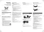
HCD-LV80
27
27
THIS NOTE IS COMMON FOR PRINTED WIRING
BOARDS AND SCHEMATIC DIAGRAMS.
(In addition to this, the necessary note is printed
in each block.)
For schematic diagrams.
Note:
• All capacitors are in µF unless otherwise noted. pF: µµF
50 WV or less are not indicated except for electrolytics
and tantalums.
• All resistors are in
Ω
and
1
/
4
W or less unless otherwise
specified.
•
f
: internal component.
•
2
: nonflammable resistor.
•
1
: fusible resistor.
•
C
: panel designation.
For printed wiring boards.
Note:
•
X
: parts extracted from the component side.
•
Y
: parts extracted from the conductor side.
•
a
: Through hole.
•
b
: Pattern from the side which enables seeing.
(The other layers' patterns are not indicated.)
•
U
: B+ Line.
•
V
: B– Line.
•
H
: adjustment for repair.
• Voltages and waveforms are dc with respect to ground
under no-signal (detuned) conditions.
• Voltages are taken with a VOM (Input impedance 10 M
Ω
).
Voltage variations may be noted due to normal produc-
tion tolerances.
• Waveforms are taken with a oscilloscope.
Voltage variations may be noted due to normal produc-
tion tolerances.
• Circled numbers refer to waveforms.
• Signal path.
F
: FM
g
: VIDEO/MD
E
: PB (DECK A)
d
: PB (DECK B)
G
: REC (DECK B)
m
: CHROMA
n
: Y
o
: VIDEO
J
: CD
c
: digital out
I
: PHONO
• Abbreviation
EA
: Saudi Arabia model.
SP
: Singapore model.
MY
: Malaysia model.
IC101
wg
MDP
1
2
3
4
WAVEFORMS
– CD SECTION –
IC101
t;
RFAC
IC101
ra
TE
IC101
el
FE
Note: The components identified by mark
0
or dotted line
with mark
0
are critical for safety.
Replace only with part number specified.
1.3Vp-p
1
2
3
IC505
ug
COUT
IC505
yl
YOUT
4
5
6
7
8
9
IC509
qj
BCLK
IC509
ql
LRCK
0
qa
IC502
qd
XOUT
Q303
E
COUT
IC401
4
YOUT
IC509
1
XT1
IC504
8
384FS
IC504
6
27M
IC504
qs
– VIDEO SECTION –
Caution:
Pattern face side: Parts on the pattern face side seen from the
(Side B)
pattern face are indicated.
Parts face side:
Parts on the parts face side seen from the
(Side A)
parts face are indicated.
– PANEL FL SECTION –
1
2
IC501
qd
XC-OUT
IC501
qa
X-OUT
– MAIN (2/3) SECTION –
IC601
us
X OUT
1
32.768kHz
5.2Vp-p
16MHz
5.5Vp-p
12.5MHz
3.4Vp-p
APPROX 500mVp-p
2.5V
APPROX 200mVp-p
2.5V
2.6Vp-p
7.5
µ
sec
4Vp-p
10MHz
H
1Vp-p
2Vp-p
H
H
1Vp-p
2Vp-p
H
27MHz
5.8Vp-p
4.8Vp-p
2.11MHz
4.6Vp-p
44.1kHz
4.8Vp-p
33.8MHz
2.8Vp-p
33.8MHz
3.8Vp-p
27MHz
• Indication of transistor
Q
C
These are omitted
E
B
B
These are omitted.
C
E
B
These are omitted.
C
E
Summary of Contents for HCD-LV80
Page 30: ...HCD LV80 30 30 7 5 SCHEMATIC DIAGRAM DECK SECTION See page 54 for IC Block Diagrams Page 38 ...
Page 31: ...HCD LV80 31 31 7 6 PRINTED WIRING BOARD DECK SECTION See page 19 for Circuit Boards Location ...
Page 39: ...HCD LV80 39 39 7 14 SCHEMATIC DIAGRAM MAIN 3 3 SECTION See page 36 for Printed Wiring Board ...
Page 41: ...HCD LV80 41 41 7 16 SCHEMATIC DIAGRAM POWER SECTION ...
Page 45: ...HCD LV80 45 45 7 20 SCHEMATIC DIAGRAM PANEL VR SECTION See page 55 for IC Block Diagrams ...
Page 47: ...HCD LV80 47 47 7 22 SCHEMATIC DIAGRAM TC PANEL SECTION ...
Page 51: ...HCD LV80 51 51 7 26 SCHEMATIC DIAGRAM CD MOTOR SECTION Page 38 ...
Page 52: ...HCD LV80 52 52 7 27 SCHEMATIC DIAGRAM TRANS SECTION ...