


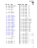


2
HCD-FX900W
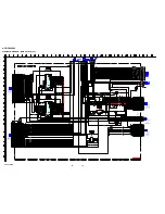
DIAGRAMS
For Schematic Diagrams.
Note:
• All capacitors are in
µ
F unless otherwise noted. (p: pF)
50 WV or less are not indicated except for electrolytics and
tantalums.
• All resistors are in
Ω
and
1
/
4
W or less unless otherwise
specified.
•
f
: internal component.
•
H
: adjustment for repair
•
A
: B+ Line.
•
B
: B– Line.
• Voltages and waveforms are dc with respect to ground un-
der no-signal (detuned) conditions.
• Voltages and waveforms are dc with respect to ground in
service mode.
• Waveforms are taken with a oscilloscope.
Voltage variations may be noted due to normal production
tolerances.
no mark : DVD STOP
• Voltages are taken with VOM (Input impedance 10 M
Ω
).
• Circled numbers refer to waveforms.
• Signal path.
F
: AUDIO
J
: CD PLAY
c
: DVD PLAY
I
: SACD PLAY
d
: TUNER
L
: VIDEO
E
: Y
a
: CHROMA
r
: COMPONENT VIDEO
f
: AUDIO IN
h
: DIGITAL IN (OPTICAL)
i
: DIGITAL IN (COAXIAL)
THIS NOTE IS COMMON FOR PRINTED WIRING BOARDS AND SCHEMATIC DIAGRAMS.
(In addition to this, the necessary note is printed in each block.)
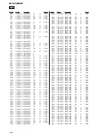
For Printed Wiring Boards.
Note:
•
a
: Through hole.
•
: Pattern from the side which enables seeing.
(The other layers' patterns are not indicated.)
• Indication of transistor.
Caution:
Parts face side: Parts on the parts face side seen from
(SIDE A) the parts face are indicated.
Pattern face side: Parts on the pattern face side seen from
(SIDE B) the pattern face are indicated.
C
B
These are omitted.
E
Q
C E
B
These are omitted
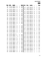
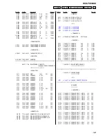
• Waveforms
– MAIN Board –
1
IC702
ws
(XIN(I))
81.3 ns
3.6 Vp-p
1 V/DIV, 40 ns/DIV
2
IC2
<zvx
(CLKIN)
40 ns
2.5 Vp-p
1 V/DIV, 20 ns/DIV
3
IC501
qg
(Xin)
200 ns
2.7 Vp-p
1 V/DIV, 100 ns/DIV
4
IC3010
rk
(XFSOIN)
20.3 ns
5.5 Vp-p
1 V/DIV, 10 ns/DIV


