


28
HCD-EA20
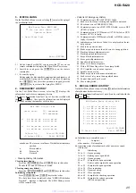
• Indication of transistor
C E
B
These are omitted
Q
C
E
B
These are omitted
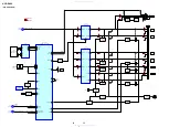
For schematic diagrams.
Note:
• All capacitors are in µF unless otherwise noted. pF: µµF
50 WV or less are not indicated except for electrolytics
and tantalums.
• All resistors are in
Ω
and
1
/
4
W or less unless otherwise
specified.
•
f
: internal component.
•
C
: panel designation.
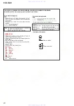
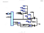
For printed wiring boards.
Note:
•
X
: parts extracted from the component side.
•
a
: Through hole.
•
b
: Pattern from the side which enables seeing.
(The other layers' patterns are not indicated.)
•
A
: B+ Line.
•
B
: B– Line.
• Voltages and waveforms are dc with respect to ground
under no-signal (detuned) conditions.
• Voltages and waveforms are dc with respect to ground in
service mode.
• Waveforms are taken with a oscilloscope.
Voltage variations may be noted due to normal produc-
tion tolerances.
no mark : STOP
• Circled numbers refer to waveforms.
• Signal path.
F
: AUDIO
J
: CD PLAY
c
: DVD PLAY
d
: TUNER
L
: VIDEO
a
: CHROMA
E
: Y
e
: AUX IN
• Abbreviation
RU
: Russian model
Caution:
Pattern face side:
Parts on the pattern face side seen from
(SIDE A)
the pattern face are indicated.
Parts face side:
Parts on the parts face side seen from
(SIDE B)
the parts face are indicated.
THIS NOTE IS COMMON FOR PRINTED WIRING BOARDS AND SCHEMATIC DIAGRAMS.
(In addition to this, the necessary note is printed in each block.)
Note: The components identified by mark
0
or dotted line
with mark
0
are critical for safety.
Replace only with part number specified.
www. xiaoyu163. com
QQ 376315150
9
9
2
8
9
4
2
9
8
TEL 13942296513
9
9
2
8
9
4
2
9
8
0
5
1
5
1
3
6
7
3
Q
Q
TEL 13942296513 QQ 376315150 892498299
TEL 13942296513 QQ 376315150 892498299


