


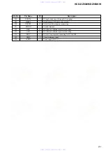

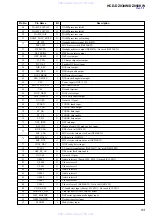


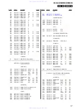


89
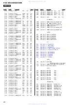
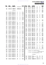
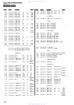
HCD-DZ830W/DZ850KW
Pin No.
Pin Name
I/O
Description
113
GND
—
Ground terminal
114
VDDINT
—
Power supply terminal (+1.2V) (for core)
115
GND
—
Ground terminal
116
VDDEXT
—
Power supply terminal (+3.3V) (for I/O)
117
GND
—
Ground terminal
118
VDDINT
—
Power supply terminal (+1.2V) (for core)
119
GND
—
Ground terminal
120
VDDINT
—
Power supply terminal (+1.2V) (for core)
121
RESET
I
Reset signal input from the system controller “L”: reset
122
SPIDS
I
Device selection signal input from the system controller
123
GND
—
Ground terminal
124
VDDINT
—
Power supply terminal (+1.2V) (for core)
125
SPICLK
I
Serial data transfer clock signal input from the system controller
126
MISO
I/O
When DSP is master: Serial data input from the flash memory
When DSP is slave: Serial data output to the main system controller
127
MOSI
I/O
When DSP is master: Serial data output to the flash memory
When DSP is slave: Serial data input from the main system controller
128
GND
—
Ground terminal
129
VDDINT
—
Power supply terminal (+1.2V) (for core)
130
VDDEXT
—
Power supply terminal (+3.3V) (for I/O)
131
AVDD
—
Power supply terminal (+1.2V) (analog system)
132
AVSS
—
Ground terminal (analog system)
133
GND
—
Ground terminal
134
CLKOUT
O
Not used (Open)
135
EMU*
O
Not used (Open)
136
TDO
O
Not used (Open)
137
TDI
I
Not used (Fixed to “L”)
138
TRST*
I
Not used (Fixed to “L”)
139
TCK
I
Not used (Fixed to “L”)
140
TMS
I
Not used (Fixed to “L”)
141
GND
—
Ground terminal
I
System clock input terminal (25 MHz)
O
System clock output terminal (25 MHz)
—
Power supply terminal (+3.3V) (for I/O)
www. xiaoyu163. com
QQ 376315150
9
9
2
8
9
4
2
9
8
TEL 13942296513
9
9
2
8
9
4
2
9
8
0
5
1
5
1
3
6
7
3
Q
Q
TEL 13942296513 QQ 376315150 892498299
TEL 13942296513 QQ 376315150 892498299


