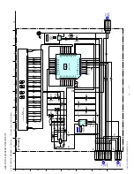


HBD-TZ210/TZ230/TZ510/TZ630/TZ710
58
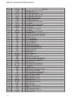
Pin No.
Pin Name
I/O
Description
218
APLLVSS
—
Ground
219
ADACVSS2
—
Ground
220
ADACVSS1
—
Ground
221
DIR_CE
—
Not used. (Open)
222
ASDATA3
—
Not used. (Open)
223
ASDATA2
O
Audio digital signal output to D-AMP
224
AVCM
—
Ext capacitor connected terminal
225
ASDATA1
O
Audio digital signal output to D-AMP
226
ASDATA0
O
Audio digital signal output to D-AMP
227
DIR_CL
—
Not used. (Open)
228
ADACVDD1
—
Power supply (+3.3V)
229
ADACVDD2
—
Power supply (+3.3V)
230
Rt/DIR_DI
—
Not used. (Open)
231
Lt/DIR_DO
—
Not used. (Open)
232
ADACVSS3
—
Ground
233
ADACVDD3
—
Power supply (+3.3V)
234
SADCVDD18
—
Power supply (+1.8V)
235
SADCVSS18
—
Ground
236
RFGND18
—
Ground
237
RFVDD18
—
Power supply (+1.8V)
238
XTALO
O
Crystal output for main clock (27MHz)
239
XTALI
I
Crystal input for main clock (27MHz)
240
JITFO
O
The output terminal of RF jitter meter
241
JITFN
I
The input terminal of RF jitter meter
242
PLLVSS
—
Ground
243
PLLVDD3
—
Power supply (+3.3V)
244
LPFON
O
The negative output of loop fi lter amplifi er
245
LPFIP
I
The positive input terminal of loop fi lter amplifi er
246
LPFIN
I
The negative input terminal of loop fi lter amplifi er
247
LPFOP
O
The positive output of loop fi lter amplifi er
248
ADCVDD3
—
Power supply (+3.3V)
249
ADCVSS
—
Ground
250
RFVDD3
—
Power supply (+3.3V)
251
RFRPDC
O
RF ripple detect output
252
RFRPAC
I
RF ripple detect input (through AC-coupling)
253
HRFZC
I
High frequency RF ripple zero crossing
254
CRTPLP
O
Defect level fi lter capacitor connected terminal
255
RFGND18
—
Power supply (+3.3V)
256
OSP
O
RF offset cancellation capacitor connecting terminal


