GXB5005
- 4 -
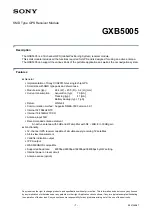
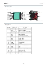
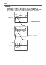
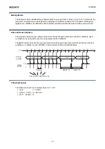
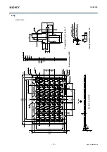
Pin Configuration
(Top View)
Pin Description
19. 1PPS
18. B.U.
17. V
DD
16. RST
15. GND
14. GND
13. Status Out
12. RF GND
11. RF IN
10. RF GND
1. AD In0
2. AD In1
3. ANT Cont
4. BR1
5. BR0
6. RXD0
7. TXD0
8. WA1
9. WA0
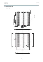
23.5mm
22.4mm
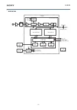
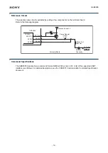
TCXO
CXD2951
Regulator
RF
32kHz X'tal
LNA
Shield Case Land
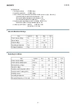
Pin No.
Symbol
I/O
Description
1
AD In0
I
Antenna sense input 0
2
AD In1
I
Antenna sense input 1
3
ANT Cont
I/O
Antenna sense enable (High active)
4
BR1
I
Baud rate setting 1
5
BR0
I
Baud rate setting 0
6
RXD0
I
UART (CH0) reception data
7
TXD0
O
UART (CH0) transmission data
8
WA1
I
WAAS enable 1
9
WA0
I
WAAS enable 0
10
RF GND
RF GND
11
RF IN
I
GPS signal input
12
RF GND
RF GND
13
Status Out
Status output
14
GND
GND
15
GND
GND
16
RST
I
Hardware reset (Low active)
17
V
DD
Power supply 3.4V
18
B.U.
Battery backup 2.8V
19
1PPS
O
1PPS output