background image

— 17 —

KV-13FM12/13FM13/13FM14/14FM12/14FM12A/14FM12C/14FM14

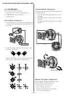
R G B B G R

R G B

R

R

R

G

B

G

B

G

B

R G B

B G R

R
G

B

R

G

B

B G R R G B

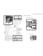
4. Tighten the deflection yoke screw.

5. Install the deflection yoke spacers.

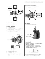
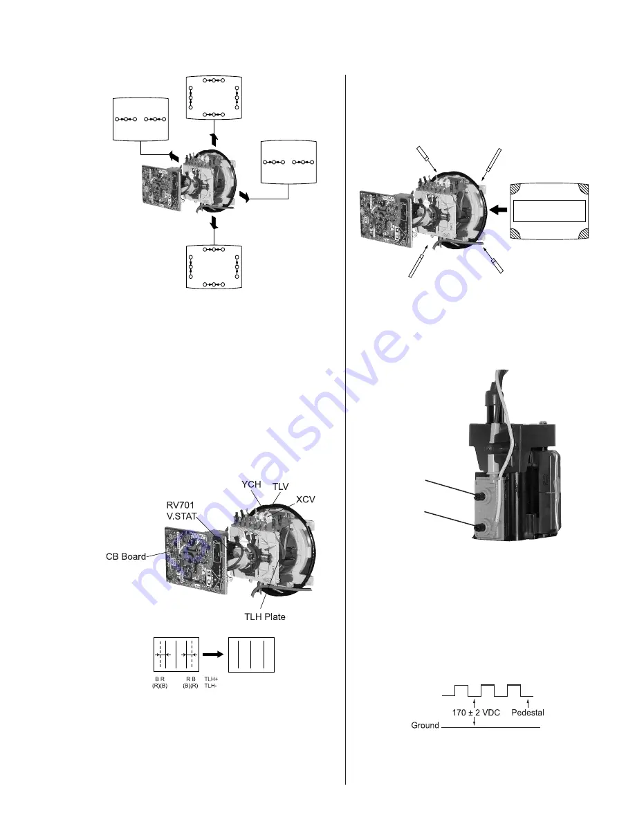
TLH Plate Adjustment

1. Input crosshatch pattern.

2. Adjust PICTURE QUALITY to standard, PICTURE and

BRIGHTNESS to 50%, and OTHER to standard.

3. Adjust the Horizontal Convergence of red and blue dots

by tilting the TLH plate on the deflection yoke.

4. Adjust XCV core to balance X axis.

5. Adjust YCH VR to balance Y axis.

6. Adjust vertical red and blue convergence with V.TILT

(TLV VR).  Perform adjustments while tracking items
1 and 2.

b

a

c

d

a

b

d

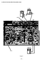
a-d: screen-corner

misconvergence

c

3-3. FOCUS

1. Adjust FOCUS control for best picture.

Focus (FV)

Screen (G2)

3-4. SCREEN (G2)

1. Input a dots pattern.

2. Set the PICTURE and BRIGHTNESS controls at minimum

and COLOR control at normal.

3. Adjust SBRT, GCUT, BCUT in service mode with an

oscilloscope as shown below so that voltages on the red,
green, and blue cathodes are 170± 2 VDC.


4. Observe the screen and adjust SCREEN (G2) VR in FBT

to obtain the faintly visible background of dot signal.

Screen-Corner Convergence

1. Affix a permalloy assembly corresponding to the

misconverged areas.

Summary of Contents for FD TRINITRON WEGA KV-13FM12

Page 1: ... KV 13FM12 RM Y172 CND SCC S41H A KV 13FM13 RM Y172 US SCC S40L A KV 13FM14 RM Y172 US SCC S40J A KV 14FM12 RM Y172 E SCC S38M A KV 14FM12A RM Y172 E SCC S38N A KV 14FM12C RM Y172 E SCC S38P A KV 14FM14 RM Y172 E SCC S38S A TRINITRON COLOR TV RM Y172 KV 14FM12A 886 Front p65 4 12 00 1 21 PM 1 ...

Page 2: ... for VHF UHF Supplied accessories Remote Commander RM Y172 SizeAA R6 batteries 2 1 1 Vp p 75 ohms unbalanced sync negative 2 500mVrms 100 modulation impedance 47kilohms KV 13FM12 KV 13FM13 KV 13FM14 KV 14FM12 KV 14FM12A KV 14FM12C KV 14FM14 Power requirements 120V 60Hz 120 220V 50 60Hz Number of inputs outputs Video 1 2 2 Audio 2 2 2 Headphone Out 1 1 Speaker output W 3W 3W Power Consumption W In ...

Page 3: ...JUSTMENTS 4 1 R564 Confirmation Method HV Hold Down Confirmation and Readjustments 19 4 2 B Voltage Confirmation andAdjustment 19 5 CIRCUIT ADJUSTMENTS 5 1 Setting the ServiceAdjustment Mode 21 5 2 Memory Write Confirmation Method 21 5 3 Adjustment Buttons and Indicators 21 5 4 MB BoardAdjustments 24 6 DIAGRAMS 6 1 Block Diagram 27 6 2 Circuit Board Location 31 6 3 Printed Wiring Boards and Schema...

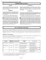
Page 4: ...CHAQUE REMPLACEMENT DE COMPOSANTS CRITIQUES OU LORSQU UN MAUVAIS FONTIONNEMENT SUSPECTE SELF DIAGNOSTIC FUNCTION The units in this manual contain a self diagnostic function If an error occurs the STANDBY TIMER LED will automatically begin to flash The number of times the LED flashes translates to a probable source of the problem A definition of the STANDBY TIMER LED flash indicators is listed in t...

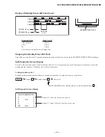
Page 5: ...ing Self Diagnostic Screen Display For errors with symptoms such as power sometimes shuts off or screen sometimes goes out that cannot be confirmed it is possible to bring up past occurrences of failure on the screen for confirmation To Bring Up Screen Test In standby mode press buttons on the Remote Commander sequentially in rapid succession as shown below Display Channel 5 Sound volume Note that...

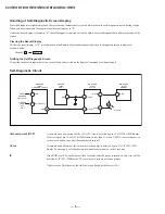
Page 6: ...nder or the main unit Self Diagnostic Circuit MB BOARD IC1301 Y CHROMA JUNGLE A BOARD IC502 V OUT MB BOARD IC1001 SYSTEM MB BOARD IC1003 MEMORY IK IN FROM CB BOARD CN705 PIN1 21 HP PROTECT SDA A BOARD FROM IC501 PIN 3 18 35 IO SDAT O LED 37 REF 3 I PROT IO BDAT 17 36 B DAT 5 18 DISPLAY B overcurrent OCP Occurs when an overcurrent on the B 135V line is detected by pin 18 of IC1301 MB Board If the v...

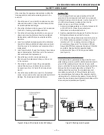
Page 7: ...round and from all exposed metal parts to any exposed metal part having a return to chassis must not exceed 0 5 mA 500 microamperes Leakage current can be measured by any one of three methods 1 A commercial leakage tester such as the Simpson 229 or RCA WT 540A Follow the manufacturers instructions to use these instructions 2 A battery operated AC milliammeter The Data Precision 245 digital multime...

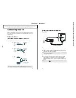
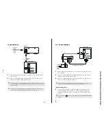
Page 8: ...g to an indoor or outdoor antenna you may need to adjust the orientation of the antenna for best reception 4 Connecting Additional Equipment TV and VCR 1 Connect the coaxial cable from your TV antenna or cable service to the IN jack on your VCR 2 Connect a coaxial cable not supplied from the OUT jack on your VCR to the VHF UHF jack on the TV Optional connection 3 If your VCR is equipped with video...

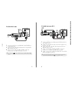
Page 9: ...of TV Coaxial Cable 6 TV VCR and Cable box 1 Connect the coaxial cable from your cable service to the IN jack on your cable box 2 Connect a coaxial cable not supplied from the OUT jack on your cable box to the IN jack on your VCR 3 Connect a coaxial cable not supplied from the OUT jack on your VCR to the VHF UHF jack on the TV Optional connection 4 If your VCR is equipped with video outputs you ca...

Page 10: ... and VCR 1 Connect the cable from your satellite antenna to SATELLITE IN on your satellite receiver 2 Connect the coaxial cable from your cable service or antenna to the IN jack on your VCR 3 Using a coaxial cable connect the OUT jack on your VCR to the VHF UHF jack on your TV 4 Using A V cables connect AUDIO and VIDEO OUT on your satellite receiver to AUDIO and VIDEO IN on your VCR 5 Using A V ca...

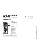
Page 11: ...TV off automatically in approximately 15 30 45 60 or 90 minutes Cancel by pressing until SLEEP OFF appears MTS SAP Cycles through the Multi channel TV Sound MTS options Stereo Mono and Auto SAP Second Audio Programming KV 21FE12 models only DISPLAY Press to display the current time if set and channel number JUMP Alternates between the last two channels selected with the buttons The remote control ...

Page 12: ...page 18 No color Adjust Color in the Video menu page 17 No signal Check the Cable setting in the Options menu under Setup page 23 Check the antenna and or cable connections page 3 Make sure the channel selected is currently broadcasting Dotted lines or stripes Adjust the antenna Move the TV away from other electronic equipment Some electronic equipment can create electrical noise which can interfe...

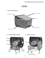
Page 13: ...EAR COVER REMOVAL 2 2 CHASSIS ASSEMBLY REMOVAL 2 3 SERVICE POSITION Screw BVTP 4x16 Screw BVTP 4x16 Rear Cover Screw BVTP 4x16 Screw BVTP 4x16 CB Board A Board MB Board Extension Cable for Service p n S 1294 965 A HC Board CB Board A Board MB Board Claw HD Board HZ Board KV 14FM12A ONLY ...

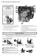
Page 14: ... 2 To avoid damaging the anode cap do not squeeze the rubber covering too hard A material fitting called a shatter hook terminal is built into the rubber 2 Use your thumb to pull the rubber cap firmly in the direction indicated by arrow b 3 When one side of the rubber cap separates from the anode button the anode cap can be removed by turning the rubber cap and pulling it in the direction of arrow...

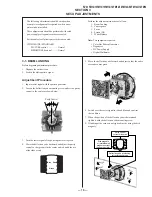
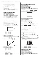
Page 15: ...red and blue and confirm the condition 7 When the position of the deflection yoke is determined tighten it with the deflection yoke mounting screw 8 If landing at the corner is not right adjust by using the disk magnets The following adjustments should be made when a complete realignment is required or when a new picture tube is installed These adjustments should be performed with rated power supp...

Page 16: ...direction of arrows a and b red green and blue dots move as shown below a b b B G R a b B G R a B G R R G B b R G B b b a R G B 1 3 2 Horizontal Static Convergence If the blue dot does not converge with the red and green dots perform the following 1 Move BMC magnet a to correct insufficient H Static convergence 2 Rotate BMC magnet b to correct insufficient V Static convergence 3 After adjusting th...

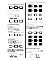
Page 17: ...lance Y axis 6 Adjust vertical red and blue convergence with V TILT TLV VR Perform adjustments while tracking items 1 and 2 b a c d a b d a d screen corner misconvergence c 3 3 FOCUS 1 Adjust FOCUS control for best picture Focus FV Screen G2 3 4 SCREEN G2 1 Input a dots pattern 2 Set the PICTURE and BRIGHTNESS controls at minimum and COLOR control at normal 3 Adjust SBRT GCUT BCUT in service mode ...

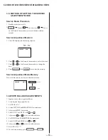
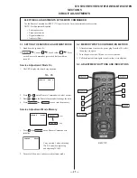
Page 18: ...ote Commander to change the data 4 Press then to save into the memory Service Adjustment Mode Memory Turn set off then on to exit service adjustment mode SERVICE WRITE Green Red MUTING ENTER 3 6 WHITE BALANCE ADJUSTMENTS 1 Input an entire white signal with burst 2 Set to ServiceAdjustment Mode 3 Set DCOL to 0 4 Set the PICTURE and BRIGHTNESS to minimum 5 Adjust with SBRT if necessary 6 Select GCUT...

Page 19: ...rease the DC power voltage gradually until the picture blanks out 6 Turn DC power source off immediately 7 Read the digital voltmeter indication standard 120 0 3 VDC 8 Input a white signal and set PICTURE and BRIGHTNESS to maximum IABL 820 100 µA 9 Repeat steps 4 to 7 Hold Down Readjustment If the setting indicated in step 2 of Hold Down Operation Confirmation cannot be met readjustment should be ...

Page 20: ...Q501 JR503 JR503 JR503 JR503 JR502 JR502 JR502 JR502 R573 R573 R573 R573 R531 R531 R531 R531 Q505 Q505 Q505 Q505 C654 C654 C654 C654 IC501 IC501 IC501 IC501 L502 L502 L502 L502 R532 R532 R532 R532 D233 D233 D233 D233 D232 D232 D232 D232 D520 D520 D520 D520 R561 R561 R561 R561 D234 D234 D234 D234 D235 D235 D235 D235 R565 R565 R565 R565 FB503 FB503 FB503 FB503 R558 R558 R558 R558 R559 R559 R559 R559...

Page 21: ...R 1 Press then on the Remote Commander to initialize SERVICE RESET 2 Turn set off then on to exit service adjustment mode SECTION 5 CIRCUIT ADJUSTMENTS Carry out step 1 when adjusting IDs 0 4 and when replacing and adjusting IC1003 5 2 MEMORY WRITE CONFIRMATION METHOD 1 After adjustment remove the power plug from theAC outlet then plug it in again 2 Turn the power switch ON and set to service mode...

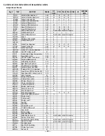
Page 22: ...t 0 15 8 8 27 VUSN V Saw Waveform Compress 0 1 0 0 28 HDW Horizontal Drive Pulse Width 0 1 1 1 29 EWDC Parabola EW D C Adjustment 0 1 0 0 30 LVLN Lower Screen BTM Vertical Line Adj 0 15 0 0 31 UVLN Uppe Screen BTM Vertical Line Adj 0 15 0 0 32 HTRP Horiz Trapezoid 0 1 0 0 33 RDRV R Output Drive control 0 63 31 21 34 GDRV G Output Drive control 0 63 21 14 35 BDRV B Output Drive control 0 63 21 14 3...

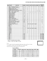
Page 23: ...08 PDSO 0 1 0 109 CK 0 1 0 110 VNL 0 15 3 3 111 HPK 0 1 0 0 112 HPK0 0 1 113 CORE 0 3 1 1 114 TRAP 0 1 1 1 115 CHTR 0 1 0 0 116 CHPF 0 1 1 1 117 ENHO 0 1 0 0 118 ID0 0 255 See ID Map 119 ID1 0 255 See ID Map 120 ID2 0 255 See ID Map 121 ID3 0 255 See ID Map 122 ID4 0 255 See ID Map 123 ID5 0 255 See ID Map 124 ID6 0 255 See ID Map VSS 1 for US CND VSS 0 for Other CDMD 3 for US CND CDMD 0 for Other...

Page 24: ...ve into the memory V Size Adjustment VSIZ 1 Input a crosshatch signal 2 Activate the ServiceAdjustment Mode 3 Select the VSIZ item with and 4 Adjust value of VPOS with and for the best vertical center 5 4 MB BOARD ADJUSTMENTS H Frequency Free Run Check 1 Input a TV mode RF with no signal 2 Connect a frequency counter to base of Q501 TP500 H DRIVE 3 Check H Frequency for 15735 200 Hz for NTSC 15650...

Page 25: ...iceAdjustment Mode 3 Select HSIZ with and 4 Adjust with and for the best horizontal size 5 Press then to save into the memory V Linearity VLIN V Correction VSCO Pin Amp PAMP and Horizontal Trapezoid TRAP Adjustments 1 Input a crosshatch signal 2 Activate the ServiceAdjustment Mode 3 SelectVLIN VSCO PAMP and PPHAwith and 4 Adjust with and for the best horizontal size 5 Press then to save into the m...

Page 26: ... 26 KV 13FM12 13FM13 13FM14 14FM12 14FM12A 14FM12C 14FM14 NOTES ...

Page 27: ... 2 H D R I V E Q 5 0 1 HD HP I N 1 EW I N 1 P I N D R I V E P I N O U T Q 5 0 4 Q 5 0 3 OUT1 I HLDWN O U T 2 S W Q 5 0 6 5 0 7 I N 2 VD DRIVE O U T GND I PROT R E F G STBY 7 5V STBY 7 I PR G MAI MAI AF AGC VD DRIVE ABL 5 V 9 V TP 508 DET OUT O M O I S I STE SE SE MU RE D C O NV ER T ER I C6 01 5 V R EG I C 60 4 9 V R E G I C6 0 3 E RR O R AM P I C6 0 2 IC 50 1 V HO L D CN TR L V O U T I C5 0 2 I C...

Page 28: ... RELAY DGC ME MO R Y IC 10 0 3 S TB Y 5V R EG I C 13 0 5 IC 1 30 4 VI DE O S W I C 13 02 D I G CO M B F I LT ER Y C J UN GL E I C 13 0 1 C R T DR I VE I C 70 2 CO N TR OL T UN IN G S YS T EM IC 1 00 1 VM VD VD EW ABL HD H P Q 1 3 2 5 1 3 2 6 F O R J I G I C 17 01 2 3 4 H E A T E R 6 H CN706 SPSW MONITOR V3 SET5V SET9V 30V SET5V SET9V 30V STBY 7 5V IR SENSOR POWER SW IK IK MENU SW GND V2 KEY SW IR ...

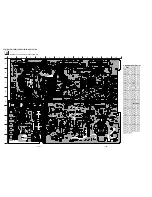
Page 29: ...lated Adjustments on page 19 When replacing parts shown in the table below be sure to perform the related adjustments 6 2 CIRCUIT BOARD LOCATIONS Part Replaced Adjustment HV HOLD DOWN R564 B VOLTAGE CONFIRMATION DY T505 CRT IC501 C507 C520 C505 C509 C515 L508 L509 C551 L510 C546 C537 C547 D517 D518 D519 R560 R561 R562 R563 R565 R566 R567 R525 A Board IC1301 MB Board IC601 PH601 A Board All voltage...

Page 30: ...503 FB503 R558 R558 R558 R558 R559 R559 R559 R559 TH501 TH501 TH501 TH501 R633 R633 R633 R633 R511 R511 R511 R511 R503 R503 R503 R503 C554 C554 C554 C554 C525 C525 C525 C525 C511 C511 C511 C511 R2015 R2015 R2015 R2015 S2003 S2003 S2003 S2003 D2002 D2002 D2002 D2002 S2004 S2004 S2004 S2004 D2001 D2001 D2001 D2001 D400 D400 D400 D400 CN408 CN408 CN408 CN408 D212 D212 D212 D212 D2005 D2005 D2005 D200...

Page 31: ...5MM 7 5MM 8mH 10k SW HDT FBT ASSY NX 1912 Q 10k 22k 33k CHIP 2 2k 22k 100 4 7 0 22 25V F 0 47 330 47k 1k 2W 22k 22 2 2 FPRD 47 220 10k 4 7 CI 20P 5P 5MM PITCH 2P AC IN 20P 4 7k PC123FY2 PHOTOCOUPLER EA135 F12 ERROR AMP 100k 10k 100k 470 10k 2 2k 220k CHIP 10k 470k 10 470k 0 47 0 22 1000p 1000p 330 470p 0 047 22 3300p 47 470p B 470p PT 0 001 1 0 01 F 0 0047 B CHIP 2SC3209LK H DRIVE 1B 2SD2624 H OUT...

Page 32: ...01 B 220p CH 220 10k 2SB601A H TRAP 2SB709A H TRAP 2SD601A SW 2SD601A HP 2SD601A HP 4 7k 4 7k 1k 22k 1k 470 100 CHIP 75 470 560 47k 3 3k CHIP 56k 560 CHIP 5 6k 22k 220 CHIP 560 CHIP 100 220 220 0 001 B 0 01 B 0 001 B 220p CH 0 001 220p CHIP 680 CHIP 2SB709A BUFFER 2SB709A BUFFER 2SB709A BUFFER 220 CHIP 220 CHIP 220 CHIP UDZ TE 17 5 1B CHIP 2SB709A IK BUFFER 2SB709A IK BUFFER 10k CHIP 2SB601A BUFFE...

Page 33: ...1360 R1360 R1364 R1364 R1364 R1364 R1362 R1362 R1362 R1362 JR1017 JR1017 JR1017 JR1017 C1354 C1354 C1354 C1354 R1359 R1359 R1359 R1359 C1340 C1340 C1340 C1340 C1042 C1042 C1042 C1042 R1060 R1060 R1060 R1060 R1074 R1074 R1074 R1074 D1011 D1011 D1011 D1011 R1063 R1063 R1063 R1063 IC1001 IC1001 IC1001 IC1001 D1012 D1012 D1012 D1012 R1080 R1080 R1080 R1080 Q1325 Q1325 Q1325 Q1325 R1405 R1405 R1405 R14...

Page 34: ...R708 R708 D702 D702 D702 D702 R712 R712 R712 R712 D701 D701 D701 D701 R710 R710 R710 R710 R709 R709 R709 R709 R711 R711 R711 R711 D703 D703 D703 D703 R713 R713 R713 R713 CN705 CN705 CN705 CN705 R700 R700 R700 R700 Q700 Q700 Q700 Q700 CN701 CN701 CN701 CN701 CN706 CN706 CN706 CN706 CN704 CN704 CN704 CN704 CN703 CN703 CN703 CN703 R721 R721 R721 R721 Q701 Q701 Q701 Q701 GAP GAP GAP GAP SPARK SPARK SP...

Page 35: ...2 2 3 3 3 3 1 1 1 1 2 2 2 2 3 3 3 3 4 4 4 4 5 5 5 5 6 6 6 6 7 7 7 7 R2201 R2201 R2201 R2201 R2203 R2203 R2203 R2203 R2204 R2204 R2204 R2204 D2201 D2201 D2201 D2201 R2205 R2205 R2205 R2205 D2202 D2202 D2202 D2202 R2206 R2206 R2206 R2206 R2207 R2207 R2207 R2207 CN2201 CN2201 CN2201 CN2201 R2202 R2202 R2202 R2202 IC2201 IC2201 IC2201 IC2201 S2201 S2201 S2201 S2201 S2202 S2202 S2202 S2202 S2203 S2203 ...

Page 36: ......

Page 37: ...s associated with the FBT on this board are not included and must be ordered separately See 23 25 19 A 1304 195 A MB VAR MOUNTED PC BOARD 20 1 783 838 31 CORD POWER WITH CONNECTOR 21 1 766 374 11 PLUG F PIN 22 1 453 339 11 FBT ASSY NX 1912 M3E4 23 25 23 1 473 159 11 HV CAP ASSY 24 1 900 800 65 FOCUS LEAD 25 1 900 803 22 G2 LEAD 26 4 076 249 01 COVER REAR 27 3 704 372 31 HOLDER HV CABLE 28 4 051 73...

Page 38: ...205 1 126 963 11 ELECT 4 7µF 20 50V C208 1 126 963 11 ELECT 4 7µF 20 50V C214 1 164 346 11 CERAMIC CHIP 1µF 16V C219 1 126 964 11 ELECT 10µF 20 50V C402 1 126 943 11 ELECT 2200µF 20 25V C403 1 126 957 11 ELECT 0 22µF 20 50V C420 1 164 222 11 CERAMIC CHIP 0 22µF 25V C442 1 126 963 11 ELECT 4 7µF 20 50V C443 1 163 009 11 CERAMIC CHIP 0 001µF 10 50V C444 1 163 021 91 CERAMIC CHIP 0 01µF 10 50V C445 1...

Page 39: ...ERAMIC CHIP 0 047µF 10 50V C644 1 161 964 91 CERAMIC 0 0047µF 250V C645 1 161 964 91 CERAMIC 0 0047µF 250V C646 1 161 964 91 CERAMIC 0 0047µF 250V C647 1 161 964 91 CERAMIC 0 0047µF 250V C648 1 136 346 21 MYLAR 0 22µF 20 125V C652 1 130 471 00 MYLAR 0 001µF 5 50V C654 1 107 636 11 ELECT 10µF 20 160V C655 1 136 311 11 MYLAR 0 47µF 20 125V ALL EXCEPT KV 14FM12A C655 1 130 711 00 FILM 0 22µF 20 250V ...

Page 40: ...521M TE1 IC501 8 759 700 07 IC NJM2903M TE2 IC502 8 759 980 58 IC TDA8172 IC601 8 749 015 60 IC STR F6624 KV 13FM12 13FM13 13FM14 ONLY IC601 8 749 013 75 IC STR F6654 ALL EXCEPT KV 13FM12 13FM13 13FM14 IC602 8 749 016 47 IC EA135 F12 IC603 8 759 198 03 IC PQ09RF21 IC604 8 759 701 75 IC NJM7805FA JACK J201 1 794 115 11 JACK BLOCK PIN 2P CHIPCONDUCTOR JR001 1 216 295 91 SHORT JR002 1 216 295 91 SHOR...

Page 41: ... 215 913 11 METAL OXIDE 220 5 3W R516 1 249 429 11 CARBON 10K 5 1 4W R517 1 249 425 11 CARBON 4 7K 5 1 4W R518 1 249 427 11 CARBON 6 8K 5 1 4W R519 1 249 427 11 CARBON 6 8K 5 1 4W R520 1 215 861 00 METAL OXIDE 47 5 1W R521 1 249 411 11 CARBON 330 5 1 4W R522 1 249 415 11 CARBON 680 5 1 4W R523 1 216 073 00 RES CHIP 10K 5 1 10W R524 1 249 429 11 CARBON 10K 5 1 4W R525 1 208 802 11 METAL CHIP 6 8K 0...

Page 42: ...2 11 CARBON 56 5 1 4W ALL EXCEPT KV 13FM12 13FM13 13FM14 R639 1 249 421 11 CARBON 2 2K 5 1 4W R640 1 249 417 11 CARBON 1K 5 1 4W R641 1 216 369 00 METAL OXIDE 1 5 2W R642 1 216 089 91 RES CHIP 47K 5 1 10W R643 1 249 419 11 CARBON 1 5K 5 1 4W R644 1 247 843 11 CARBON 3 3K 5 1 4W R645 1 215 898 11 METAL OXIDE 10K 5 2W R646 1 249 419 11 CARBON 1 5K 5 1 4W R648 1 215 908 00 METAL OXIDE 33 5 3W R650 1 ...

Page 43: ...1 215 888 00 METAL OXIDE 220 5 2W R720 1 249 421 11 CARBON 2 2K 5 1 4W R721 1 249 421 11 CARBON 2 2K 5 1 4W VARIABLE RESISTOR RV701 1 241 656 11 RES ADJ METAL FILM 110M A 1372 814 A HC VAR MOUNTED PC BOARD ALL EXCEPT KV 14FM12A A 1372 813 A HC VAR MOUNTED PC BOARD KV 14FM12A ONLY CONNECTOR CN2201 1 564 522 11 PLUG CONNECTOR 7P A 1332 062 A CB VAR MOUNTED PC BOARD 4 382 854 11 SCREW M3X10 P SW CAPA...

Page 44: ...OR CN2210 1 564 523 11 PLUG CONNECTOR 8P CN2211 1 564 518 11 PLUG CONNECTOR 3P CN2212 1 564 518 11 PLUG CONNECTOR 3P CN2213 1 564 522 11 PLUG CONNECTOR 7P DIODE D2211 8 719 108 12 DIODE RD9 1EW T1 D2212 8 719 110 17 DIODE MTZJ T 77 10B D2213 8 719 924 13 DIODE MTZJ T 77 22B JACK J2211 1 794 266 21 JACK PIN 2P J2212 1 568 267 21 JACK RESISTOR R2211 1 249 419 11 CARBON 1 5K 5 1 4W R2212 1 249 421 11...

Page 45: ...CERAMIC CHIP 0 01µF 10 50V C1306 1 126 933 11 ELECT 100µF 20 16V C1307 1 163 021 91 CERAMIC CHIP 0 01µF 10 50V C1308 1 126 933 11 ELECT 100µF 20 16V C1309 1 163 021 91 CERAMIC CHIP 0 01µF 10 50V C1310 1 163 021 91 CERAMIC CHIP 0 01µF 10 50V C1311 1 163 038 91 CERAMIC CHIP 0 1µF 25V C1313 1 163 021 91 CERAMIC CHIP 0 01µF 10 50V C1315 1 163 021 91 CERAMIC CHIP 0 01µF 10 50V C1320 1 163 021 91 CERAMI...

Page 46: ... D1013 8 719 977 22 DIODE UDZ TE 17 9 1B D1014 8 719 073 01 DIODE MA111 TX D1301 8 719 914 44 DIODE DAP202K T 146 D1310 8 719 976 99 DIODE UDZ TE 17 5 1B FERRITE BEAD FB1302 1 412 911 11 FERRITE 0µH FILTER FL1301 1 239 847 11 FILTER LOW PASS FL1302 1 239 847 11 FILTER LOW PASS FL1303 1 239 847 11 FILTER LOW PASS IC IC1001 8 759 670 42 IC M37273MF 259SP IC1003 8 759 527 77 IC M24C16 MN6T IC1301 8 7...

Page 47: ... 00 RES CHIP 220 5 1 10W R1025 1 208 814 91 METAL CHIP 22K 0 50 1 10W R1026 1 216 065 91 RES CHIP 4 7K 5 1 10W R1027 1 216 041 00 RES CHIP 470 5 1 10W R1028 1 216 045 00 RES CHIP 680 5 1 10W R1029 1 216 113 00 RES CHIP 470K 5 1 10W R1030 1 216 049 91 RES CHIP 1K 5 1 10W R1031 1 216 041 00 RES CHIP 470 5 1 10W R1032 1 216 065 91 RES CHIP 4 7K 5 1 10W R1033 1 216 081 00 RES CHIP 22K 5 1 10W R1034 1 ...

Page 48: ...P 22K 5 1 10W R1331 1 216 049 91 RES CHIP 1K 5 1 10W R1332 1 216 043 91 RES CHIP 560 5 1 10W R1333 1 216 033 00 RES CHIP 220 5 1 10W R1334 1 216 025 91 RES CHIP 100 5 1 10W R1335 1 216 025 91 RES CHIP 100 5 1 10W R1336 1 216 053 00 RES CHIP 1 5K 5 1 10W R1338 1 216 091 00 RES CHIP 56K 5 1 10W R1342 1 216 025 91 RES CHIP 100 5 1 10W R1344 1 216 025 91 RES CHIP 100 5 1 10W R1345 1 216 049 91 RES CHI...

Page 49: ...IP 4 7K 5 1 10W R1409 1 216 043 91 RES CHIP 560 5 1 10W R1410 1 216 295 91 SHORT ALL EXCEPT KV 14FM12A R1411 1 216 033 00 RES CHIP 220 5 1 10W R1413 1 216 091 00 RES CHIP 56K 5 1 10W R1414 1 216 049 91 RES CHIP 1K 5 1 10W R1415 1 216 049 91 RES CHIP 1K 5 1 10W R1416 1 216 057 00 RES CHIP 2 2K 5 1 10W R1417 1 216 035 00 RES CHIP 270 5 1 10W R1418 1 216 045 00 RES CHIP 680 5 1 10W R1419 1 216 295 91...

Page 50: ... 65 KV 13FM12 13FM13 13FM14 14FM12 14FM12A 14FM12C 14FM14 NOTES ...

Page 51: ... 66 KV 13FM12 13FM13 13FM14 14FM12 14FM12A 14FM12C 14FM14 NOTES ...

Page 52: ... 67 KV 13FM12 13FM13 13FM14 14FM12 14FM12A 14FM12C 14FM14 ...

Page 53: ...KV 13FM12 13FM13 13FM14 14FM12 14FM12A 14FM12C 14FM14 Sony Corporation Sony Technology Center Product Quality Division Service Promotion Dept 9 965 886 01 English 2000ES74324 1 Printed in USA 2000 4 ...

Page 54: ...ual Section 6 Block Diagrams Page 27 30 Size of Block Diagrams increased and replaced MODEL COMMANDER DEST CHASSIS NO KV 13FM12 RM Y172 US SCC S40H A KV 13FM12 RM Y172 CND SCC S41H A KV 13FM13 RM Y172 US SCC S40L A KV 13FM14 RM Y172 US SCC S40J A KV 14FM12 RM Y172 E SCC S38M A KV 14FM12A RM Y172 E SCC S38N A KV 14FM12C RM Y172 E SCC S38P A KV 14FM14 RM Y172 E SCC S38S A ...

Page 55: ...V STBY 7 5V I PROT GND MAIN 1 MAIN 2 AFT AGC MUTE VD D R I V E ABL 5V 9V TP 508 DET OUT O MON0 O SAP I SAP I STEREN SEL 0 SEL 1 MUTE HP RELAY DGC CONVERTER IC601 5V REG IC604 9V REG IC603 ERROR AMP IC602 IC501 V HOLD CNTRL V OUT IC502 IC402 MEMORY IC1003 STBY 5V REG IC1305 IC1304 VIDEO SW IC1302 DIG COMB FILTER Y C JUNGLE IC1301 CRT DRIVE IC702 CONTROL TUNING SYSTEM IC1001 VM VD VD EW ABL HD AC AC...

Page 56: ...9 965 886 91 Sony Corporation SonyTechnologyCenter ProductQualityDivision Service Promotion Department English 2000FJ74324 1 Printed in U S A 2000 6 KV 13FM12 13FM13 13FM14 14FM12 14FM12A 14FM12C 14FM14 ...
Reviews: