background image

1-3


8


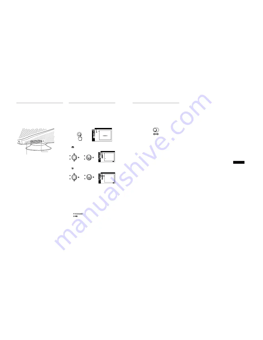
Connecting Universal Serial Bus 
(USB) compliant peripherals


Your monitor has one upstream and four downstream USB 
connectors. They provide a fast and easy way to connect USB 
compliant peripheral devices (such as keyboards, mice, printers 
and scanners) to your computer using a standardized USB cable.
To use your monitor as a hub for your peripheral devices, connect 
the USBs as illustrated below.


1


Turn on the monitor and computer.


2


Connect your computer to the square upstream 
connector using the supplied USB cable.


For customers using Windows


If a message appears on your screen, follow the on-screen instructions 
and select Generic USB Hub as the default setting.


3


Connect your USB compliant peripheral devices to 
the rectangular downstream USB connectors.


Notes


• Not all computers and/or operating systems support USB 

configurations. Check your computer’s instruction manual to see if you 
can connect USB devices.

• In most cases, USB driver software needs to be installed on the host 

computer. Refer to the peripheral device’s instruction manual for 
further details.

• The monitor functions as a USB hub as long as the monitor is either 

“on” or in power saving mode.

• If you connect a keyboard or mouse to the USB connectors and then 

boot your computer for the first time, the peripheral devices may not 
function. First connect the keyboard and mouse directly to the 
computer and set up the USB compliant devices. Then connect them to 
this monitor.


Selecting the on-screen menu 
language (LANGUAGE)


English, French, German, Spanish, Italian, Dutch, Swedish, 
Russian and Japanese versions of the on-screen menus are 
available. The default setting is English.


1


Press the MENU button.


The menu appears on the screen.


2


Move the control button up or down to highlight 

 OPTION and press the control button. 


3


Move the control button up or down to highlight 

 LANGUAGE and press the control button.


4


Move the control button up or down until the desired 
language appears on the screen. Then press the 
control button to select the language.


Each time you move the control button up or down, the 
language can be selected appears cyclically.
• ENGLISH
• FRANÇAIS: French
• DEUTSCH: German
• ESPAÑOL: Spanish
• ITALIANO: Italian
• NEDERLANDS: Dutch
• SVENSKA: Swedish

: Russian

: Japanese 


To close the menu


Press the MENU button. If no buttons are pressed, the menu closes 
automatically after about 45 seconds.


To reset to English


Select ENGLISH in step 4 above.

to USB compliant 
peripheral devices

to a USB compliant 
computer

MENU

CONTRAST

CONTRAST

50

/

I

BR GHT

1 0 2 4 x 7 6 8   /     8 5 H z

b

OK

MENU

E

OPT ON

I

CONTROL
LOCK

OFF

ON

X I T :

b

b

OK

OK

OPT ON

I

LANGUAGE

ENGL I SH

MENU

EX I T :

b

b

OK


9

US


Selecting the input signal


You can connect two computers to this monitor using the video 
input 1 (HD15) and video input 2 (BNC) connectors. To select 
one of the two computers, use the INPUT switch.


Move the INPUT switch.


The selected connector appears on the screen for 3 seconds.

“INPUT 1”: HD15 or “INPUT 2”: BNC appears on the screen.


Note


If no signal is input to the selected connector, NO SIGNAL appears on the 
screen. After a few seconds, the monitor enters the power saving mode. If 
this happens, switch to the other connector.

INPUT

1

2

Summary of Contents for CPD-G52

Page 1: ...291 mm w h 15 3 8 11 1 2 inches or Approx 364 291 mm w h 14 3 8 11 1 2 inches Deflection frequency Horizontal 30 to 130 kHz Vertical 48 to 170 Hz AC input voltage current 100 to 240 V 50 60 Hz 2 0 1 0 A Power consumption Approx 135 W with no USB devices connected Dimensions Approx 497 502 485 mm w h d 19 5 8 19 18 7 8 inches Mass Approx 30 kg 66 lb 2 oz Plug and Play DDC2B DDC2Bi GTF Recommended h...

Page 2: ... which though functioning show obvious signs of deterioration Point them out to the customer and recommend their replacement 6 Check the line cords for cracks and abrasion Recommend the replacement of any such line cord to the customer 7 Check the B and HV to see if they are specified values Make sure your instruments are accurate be suspicious of your HV meter if sets always have low HV 8 Check t...

Page 3: ...al Protection Agency Power mode Power consumption power indicator normal operation 135 W CPD G520 130 W CPD G420 green active off deep sleep 3 W orange power off Approx 0 W off DIAGNOSIS Failre B failure Horizontal Vertical Deflection failure Thermal protector ABL protector HV failure Aging Self Test Out of scan range Power LED Amber Off 0 5 sec 0 5 sec Amber Off 1 5 sec 0 5 sec Amber Off 0 5 sec ...

Page 4: ...H BLK 6 356 2 440 2 152 2 424 H FP 0 636 0 279 0 457 0 485 H SYNC 3 813 0 837 0 622 0 754 H BP 1 907 1 325 1 073 1 185 H ACTIV 25 422 6 972 5 630 6 465 VERTICAL V FREQ HZ 59 940 Hz 85 000 Hz 84 977 Hz 75 000 Hz lines lines lines lines V TOTAL 525 1250 1512 1500 V BLK 45 50 72 60 V FP 10 1 1 1 V SYNC 2 3 3 3 V BP 33 46 68 56 V ACTIV 480 1200 1440 1440 SYNC INT G NO NO NO NO EXT H V POLARITY YES N N...

Page 5: ...or Removal 2 3 2 5 D Board Removal 2 3 2 6 Service Position 2 4 2 7 Picture Tube Removal 2 5 2 8 Harness Location 2 6 3 SAFETY RELATED ADJUSTMENT 3 1 4 ADJUSTMENTS 4 1 5 DIAGRAMS 5 1 Block Diagrams 5 1 5 2 Frame Schematic Diagram 5 7 5 3 Circuit Boards Location 5 9 5 4 Schematic Diagrams and Printed Wiring Boards 5 9 1 Schematic Diagram of A1 Board 5 11 2 Schematic Diagram of US Board Only NH SH E...

Page 6: ...e of the tilt swivel This monitor can be adjusted within the angles shown below To find the center of the monitor s turning radius align the center of the monitor s screen with the centering dot on the stand Hold the monitor at the bottom with both hands when you turn it horizontally or vertically Be careful not to pinch your fingers at the back of the monitor when you tilt the monitor up vertical...

Page 7: ... cable supplied to video output AC IN 1 2 R G B HD VD to R G B input to HD VD input Refer to the preceding examples to connect to your computer video signal cable SMF 400 not supplied 7 US Step 2 Connect the power cord With the monitor and computer switched off first connect the power cord to the monitor then connect it to a power outlet Step 3 Turn on the monitor and computer First turn on the mo...

Page 8: ...guage LANGUAGE English French German Spanish Italian Dutch Swedish Russian and Japanese versions of the on screen menus are available The default setting is English 1 Press the MENU button The menu appears on the screen 2 Move the control button up or down to highlight OPTION and press the control button 3 Move the control button up or down to highlight LANGUAGE and press the control button 4 Move...

Page 9: ...language changing the on screen menu position changing the picture s color temperature setting mode 8 RESET page 18 Resets the adjustments MENU E COLOR 5 0 0 0 K X I T EASY MENU E OPT ON I CONTROL LOCK OFF ON X I T MENU E RESET CURRENT MODE CANCEL OK 1 2 X I T CONTRAST CONTRAST 50 I BR GHT 1024x768 85Hz the vertical frequencies of the current input signal the horizontal frequencies resolution of t...

Page 10: ...R GHT MENU EX I T 13 US Automatically sizing and centering the picture AUTO You can easily adjust the picture to fill the screen by using the SIZE CENTER menu 1 Press the MENU button The menu appears on the screen 2 Move the control button up or down to highlight SIZE CENTER and press the control button The SIZE CENTER menu appears on the screen 3 Move the control button up or down to select AUTO ...

Page 11: ... or blue shadows T TOP vertically shift red or blue shadows at the top of the screen B BOTTOM vertically shift red or blue shadows at the bottom of the screen 0 RESET reset all the CONVERGENCE adjustments to the factory setting levels Select OK 15 US Moire is a type of natural interference which produces soft wavy lines on your screen It may appear due to interference between the pattern of the pi...

Page 12: ...us allows you to restore the color to the original factory quality levels The explanation below explains how to restore the monitor s color from the EASY mode for example First select the EASY PRESET or sRGB mode in the OPTION menu page 15 1 Press the MENU button The menu appears on the screen 2 Move the control button up or down to highlight COLOR and press the control button The COLOR menu appea...

Page 13: ...eshooting Before contacting technical support refer to this section If thin lines appear on your screen damper wires The visible lines on your screen especially when the background screen color is light usually white are normal for the Trinitron monitor This is not a malfunction These are shadows from the damper wires used to stabilize the aperture grille The aperture grille is the essential eleme...

Page 14: ...e degree of moire cancellation until the moire is minimal or set CANCEL MOIRE to OFF page 14 21 US If a second degauss cycle is needed allow a minimum interval of 20 minutes for the best result A humming noise may be heard but this is not a malfunction Picture is ghosting Eliminate the use of video cable extensions and or video switch boxes Check that all plugs are firmly seated in their sockets P...

Page 15: ...RGB 0 700 Vp p positive 75 Ω SYNC signal H V separate or composite sync TTL 2 kΩ Polarity free Sync on Green 0 3 Vp p negative Standard image area Approx 388 291 mm w h 15 3 8 11 1 2 inches or Approx 364 291 mm w h 14 3 8 11 1 2 inches Deflection frequency Horizontal 30 to 130 kHz Vertical 48 to 170 Hz AC input voltage current 100 to 240 V 50 60 Hz 2 0 1 0 A Power consumption Approx 135 W with no ...

Page 16: ...MI shield 4 Three screws BVTT 4 x 8 5 Three screws BVTT 4 x 8 2 Two claws Bezel assembly Bezel assembly EMI shield Cabinet Cabinet Push in the tip of a screwdriver about 10mm to unlock the claw B A C 3 Push the upper side of the cabinet in the direction of arrow A disconnect claws then remove the cabinet lifting it up in the direction of arrow B 1 A1 board C BLOCK CN315 CN318 GND GND ...

Page 17: ... Video case 8 A1 board CN315 NH SH EQ MODEL 5 1 Two screws BVTT 4 x 8 2 Video block assembly 11 Screw BVTT 4 x 8 13 Gasket USB 14 Five screws BVTT 3 x 8 15 USB case 16 US board 12 USB block assembly CN315 CN2601 3 Four screws BVTP 3 x 8 Screw BVTP 3 X 10 9 Video case 8 Input out terminal board assembly CN313 6 Two screws BVTP 3 X 8 7 Two screws HEX 10 A1 board 4 Video shield ...

Page 18: ...ube shield Before removing the bezel assembly secure the picture tube by attaching two screws to the picture tube shield at the positions shown with an arrow diagonal two places to prevent the picture tube from falling Use the screws BVTT 4 x 8 that fix EMI shield 1 A1 board C block 2 Two screws BVTT 4 x 6 4 Two screws BVTP 3 x 10 D board 3 Video block assembly 5 Rear plate assembly 6 Five screws ...

Page 19: ... Remove the Video block assembly 3 Install the Adaptor board XT MOUNT A 1391 123 A 4 Lay the Video block assembly Video block assembly Video block assembly 5 5 Install the video block assembly 6 Put a box which is about 15cm in height under the D board to fix it D board Box ...

Page 20: ...in the rubber 3 Don t turn the foot of rubber over hardly The shatter hook terminal will stick out or damage the rubber REMOVAL OF ANODE CAP NOTE Short circuit the anode of the picture tube and the anode cap to the metal chassis CRT shield or carbon painted on the CRT after removing the anode REMOVING PROCEDURES 1 Turn up one side of the rubber cap in the direction indicated by the arrow a 2 Using...

Page 21: ...12 CN311 CN318 CN319 CN320 CN316 CN315 CN303 CN1103 CN1400 CN1500 CN1401 CN605 CN701 CN501 CN1601 CN1600 CN1602 CN2 CN1 CN1 5P CN3 CN1003 CN904 CN2601 4P 4P D board A1 board N board L2 board Magnetic sensor US board NH SH EQ model H1 board Picture tube AC inlet 3P ...

Page 22: ... D board is 17 0 V or more b HV Protector Circuit Check 1 Using external DC Power Supply apply the voltage shown below between cathode of D912 and GND and check that the RASTER disappers Specification 19 95 0 00 0 05 V c Beam Current Protector Circuit Check 1 Connect constant current source to a section between T901 FBT qa pin and GND and check that the RASTER disappers when the specified current ...

Page 23: ...nge LCC_NS 128 15 LCC_LT LCC_LB LCC_RT and LCC_RB 128 40 Set LCC_SW to 13 and Perform Service Save 17 Adjust top and bottom pins correction VR 18 Adjust the horizontal trapezoid distortion by DY horizontal trapezoid correction VR 19 Check landing at each corner and in case not in specification adjust landing of 4 corners with LCC_NS LCC_LT LCC_LB LCC_RT and LCC_RB The limitations of registers are ...

Page 24: ...nvex parts of 6 pole magnet for convergence together 3 Roughly adjust H CONV and V CONV with 4 pole magnet White Balance Adjustment Specification 1 9300 K x 0 283 0 005 y 0 298 0 005 All White 2 6500 K x 0 313 0 005 y 0 329 0 005 All White 3 5000 K x 0 346 0 005 y 0 359 0 005 All White Vertical and Horizontal Position and Size Specification Focus adjustment Adjust the focus volume 1 and 2 for the ...

Page 25: ... 5V CN312 G2 1 G2 CN318 5 3 1 7 KR KG KB HEATER CN315 5 3 1 7 KR KG KB HEATER FV FC HV CN318 V901 PICTURE TUBE 7 10 17 18 11 10 2 C TO D BOARD CN604 TO D BOARD FBT A1 VIDEO AMP RGB OUT H1 USER CONTROL L2 CY LCC R_IK G_IK B_IK B SS3549 NH BD1 EPS05 Vcc OUT VADJ 7V 10 11 12 7 8 9 1 4 15 16 2 3 13 DDC GND1 DDC SCL1 DDC SDA1 DDC GND2 DDC SCL2 DDC SDA2 H BLK INPUT SW IIC SCL IIC SDA HS OUT VS OUT ECO S...

Page 26: ...9 11 13 15 17 29 1 3 2 4 35 33 31 39 40 6 8 10 12 14 16 18 24 26 28 23 25 30 36 5 LB DET IK SIGMA DDC SDA1 DDC SCL1 DDC GND1 DDC SDA2 DDC SCL2 DDC GND2 INPUT SW IIC SDA IIC SCL TXD RXD KEY SCAN LED1 LED2 PLL LOCK POC HV DET ABL DET G2 S6 S5 S4 S3 S2 S1 S0 PWR SW DGC SW V FBP WAKE UP ECO SW IC1001 CPU P42 AN10 P41 AN09 P86 SDA1 P87 SCL1 P21 A1 A17 P84 SDA2 P85 SCL2 P20 A0 A16 P27 A7 A23 P80 SDA0 SI...

Page 27: ...05 V DF OUT Q706 707 T701 DFT CN605 1 2 7V 7V B 80V 12V 7V 3 3V 5V 7V I TO N BOARD CN1001 32 34 7 9 11 13 15 17 5 29 1 3 2 4 36 35 33 31 39 40 6 8 10 12 14 16 18 24 26 28 23 25 30 LB DET IK SIGMA DDC SDA1 DDC SCL1 DDC GND1 DDC SDA2 DDC SCL2 DDC GND2 ECO SW INPUT SW IIC SDA IIC SCL TXD RXD WAKE UP KEY SCAN LED1 LED2 PLL LOCK POC HV DET ABL DET G2 S6 S5 S4 S3 S2 S1 S0 PWR SW DGC SW V FBP IIC SDA IIC...

Page 28: ...2 CY LCC DA DPU A1 VIDEO AMP RGB OUT CN1101 40P 40 39 38 37 36 35 34 33 32 31 30 29 28 27 26 25 24 23 22 21 20 19 18 17 16 15 14 13 12 11 10 9 8 7 6 5 4 3 2 1 CN502 40P 40 39 38 37 36 35 34 33 32 31 30 29 28 27 26 25 24 23 22 21 20 19 18 17 16 15 14 13 12 11 10 9 8 7 6 5 4 3 2 1 XSC YSC D TILT XDC HFBP YDC HD OUT REFDC HSHAPE 12V NC 12V A GND 3 3V D GND D GND HSAW_SW GXSC LCC NS GYSC IIC SDA IIC S...

Page 29: ...ariations may be noted due to normal production tolerances Can not be measured Circled numbers are waveform references s B bus S B bus G D S 2 3 4 5 6 7 8 9 0 qa qs qf qh 1 G D S G S S D G D Ver 1 6 Transistor FET Transistor Transistor Discrete semiconductot Chip semiconductors that are not actually used are included Diode Diode Diode Diode Diode Diode Diode Diode Diode Diode Source Source Anode A...

Page 30: ...S119 R031 15k CHIP R058 1k CHIP C032 0 1 25V B CHIP CN309 5 4 3 2 1 10 9 8 7 6 15 14 13 12 11 D301 1PS226 115 1 2 IC007 BR24C21F ROM NC NC 3 4 6 5 7 8 SDA SCL VCLK VCC GND NC 1 2 IC006 SN74AHCT04NSR INVERTER Y1 A1 3 7 12 8 13 14 Y4 Y6 A6 VCC GND A2 4 5 A3 Y2 6 9 10 11 A4 Y5 A5 Y3 1 2 ROM NC NC 3 4 6 5 7 8 SDA SCL VCLK VCC GND NC D012 1PS226 115 C320 47 25V R301 82 1 4W RN CP R340 33 D101 1PS226 11...

Page 31: ... IC IC001 A 3 IC002 A 3 IC003 A 2 IC004 A 4 IC005 A 2 IC006 A 1 IC007 B 1 IC008 A 1 IC009 B 1 IC011 B 3 TRANSISTOR Q101 A 3 1 Q201 A 3 1 Q301 A 3 1 DIODE D001 B 1 8 D002 B 1 D003 B 2 D004 B 1 6 D005 B 1 6 D006 B 1 8 D007 B 2 D008 B 2 D009 B 1 D010 B 1 D011 B 1 D012 B 1 6 D013 B 1 D014 C 2 D016 B 1 D019 A 1 6 D101 A 1 6 D104 A 4 3 D105 A 3 3 D106 A 4 D108 A 3 10 D111 B 1 6 D201 A 1 6 D204 A 4 2 D20...

Page 32: ...2 16V B CHIP C2915 0 22 16V B CHIP 27p 22p 0 22 16V B CHIP C2923 0 01 B CHIP PST600J T RESET 0 1 25V B CHIP 47 25V 25V C2901 0 1 B CHIP PQ3TZ53U 5V REG UDZS TE 17 5 6B 4P C2611 47 C2604 10 25V C2609 220 10V D D V BUS1 V BUS1 D 1 D 1 V BUS2 D 2 D 2 V BUS3 D 3 D 3 GND3 D 4 D 4 V BUS4 GND1 GND2 GND4 GND 1 2 3 4 UP_DP UP_DM DWN_DP_1 DWN_DM_1 DWN_DM_2 DWN_DP_2 DWN_DP_3 DWN_DM_3 DWN_DP_4 DWN_DM_4 US USB...

Page 33: ...B CHIP STZ6 8 STZ6 8 180k RN CP 22k RN CP STZ6 8 100p CH CHIP 1k CHIP 4700p B CHIP 6800p B CHIP 47k RN CP 8 2k RN CP CXD9563Q 100p CH CHIP 40P 0 15 16V B CHIP 680p B CHIP 1SS357 HD OUT H FBP DCC2 HDF REF DC XDC GYSC GXSC VDF YSC XSC HSHAPE YDC HCENT HLINBAL SCL SDA PLL LOCK HS OUT VS OUT H BLK SCL SDA PLL LOCK HS OUT VS OUT H BLK REF DC XDC D TILT POC HD OUT H FBP POC YDC VDF HDF H FBP HD OUT HSAW...

Page 34: ...3 S4 S5 S6 ECO SW V FBP T AMB VX VY HV DET ABL DET LOCK SDA SCL TXD RXD DEGAUSS HEATER REMOTE VY VX T AMB IK SIGMA ABL DET INPUT SW S0 S1 S2 S3 S4 S5 S6 ECO SW V FBP HV DET REMOTE HEATER DEGAUSS LB DET LED2 LED2 LED1 LED1 KEY SCAN S7 S7 POC FAN SW WAKE UP WAKE UP LUMI LUMI DSDA1 DSCL1 DDC GND1 DSDA2 DSCL2 DDC GND2 DDC GND1 DDC GND2 5V 5V 5V 5V 5V 5V 5V T_AMB VY VX GND VREFH P42 AN11 P41 AN09 P42 A...

Page 35: ...C D GND GYSC 3 3V A GND 12V 12V REFDC HD OUT YDC HFBP XDC D TILT XSC TO DA BOARD CN1101 IIC SDA TXD IIC SCL RXD ECO SW HV DET ABL DET GND GND S0 GND HTR SW PWR SW DGS SW S1 5V INPUT SW V FBP LED2 LB DET LED1 IK SIGMA KEY SCAN GND PLL LOCK POC NC NC NC S7 NC G2 S6 S5 S4 S3 S2 GND LCC NS HSAW_SW WAKE UP V H DY V DY V NC H NC H DDC SDA1 DDC SCL1 DDC GND1 DDC SDA2 DDC SCL2 DDC GND2 YDC YDC XDC XDC YSC...

Page 36: ...X UDZS TE17 10B 1SS119 MA111 TX MA111 TX 1 1µH 0 CHIP 0 CHIP 0 CHIP BA9758AFS E2 NJM2904M TE2 2SC2362KG AA 2SC3421 Y 2SA1358 Y 2SA1037AK 10k CHIP 1k CHIP 1k CHIP 470 FPRD 4 7 FPRD 4 7 FPRD 15 2W RS 2 2k CHIP 10 FPRD 68k CHIP 100k CHIP 47k CHIP 180k RN CP 2 2k CHIP 1k CHIP 4 7k CHIP 68 10W RN 22 FPRD 47 FPRD 2 2 FPRD 820k 1 2W RN 10k CHIP 56k RN CP 4 7k 10k RN CP 270k RN CP 27k CHIP 4 7k 1 2W RC 33...

Page 37: ...00V 8200p 800V PP 47 16V 220 10V 4700p PT 0 1 MPS 4P WHT VH 3P WHT VH 9P BLK D4SB60L RM11A D1NL20U TR P6KE200AG23 ERB38 06V1 D1NL20U TR RD27ES T1B ERB38 06V1 MA111 MA111 D4SBL40 D1NL20U TR D4SBS4 1SS119 25TD 1SS119 25TD 1SS119 25TD MA111 TX 6 3A MCZ3001D FA13842P NJM7812FA 2SK2647 01MR F91 Q640 2SK2876 01MR F122 DTC114ESA TP 0 33 2W 0 47 2W 100 100 6 8k 10k CHIP 1k CHIP 0 1 1 2W RF 1 FPRD 22k CHIP...

Page 38: ...6 E 1 Q517 E 1 Q519 D 2 1 Q521 C 1 1 Q523 C 1 1 Q524 D 2 1 Q610 A 2 Q611 B 7 Q630 B 4 Q640 A 3 Q641 A 3 Q652 A 2 Q701 D 4 Q702 D 4 Q703 D 5 Q704 D 5 Q705 D 5 Q706 E 6 Q707 E 6 1 Q901 C 5 Q902 C 6 Q903 D 5 1 Q904 D 5 1 Q905 D 6 Q906 D 6 1 Q907 D 6 1 DIODE D401 D 4 D405 C 4 D406 D 4 D501 E 1 D502 E 3 D503 D 3 D504 E 4 D505 D 2 D506 E 2 D509 C 1 3 D510 E 4 D512 D 2 D516 D 3 D517 E 4 D518 C 1 D519 C 1...

Page 39: ...6 R1406 R1407 R1419 R1420 R1422 R1423 TH1400 CN1400 DTC114ESA TP DTA124ESA 47 16V 47 16V 10 0 1 B 220 RN 220 RN 100 RN 100 RN 470 RN 100k 470 10k RN 22k RN 100k SML79423C TP15 H1 USER CONTROL DTC114TSA MENU PICTURE MODE OK VY VX GND 12V 5V KEY SCAN LED 1 TO D b BOARD CN1106 LED 2 GND 5V INPUT SW 12V GND VX VY T_AMB GND GND WAKE UP INPUT1 INPUT2 A G POWER 16V 16V 16V 10k 0 01 47 16V 47 16V 5P 1SS11...

Page 40: ...P YEL S MICRO 1 1µH 10k CHIP 0 1 B CHIP 0 1 B CHIP 10 16V 0 1 25V F CHIP 47 25V 47 25V 47 25V 1 2 FPRD 1 2 FPRD 47 25V 1 2 FPRD 1 2 FPRD 22 1W RS LA6500 FA AMP 5V REG IC1605 NJM78L05 0 01 B CHIP 15k CHIP 4 7k CHIP 18k CHIP 1 5k CHIP 100 CHIP 100 CHIP LA6510 AMP LA6510 AMP MB88141PF 8P WHT GYSC GXSC LCCRT LCCRB LCCLT GYSC GXSC LCCLB LCCLB LCCLT LCCRB LCCRT V S1 OUT1 VCC V S2 VEE OUT2 V S1 OUT1 VCC ...

Page 41: ...5 2PD602AR 115 2SA1037AK T146 QR 2SA1037AK T146 R 2SA1162 G 2SB709A QRS TX 2SC1623 L5L6 2SC2412K T 146 QR DTA124ESA TP DTC114ESA DTC114ESA TP DTC143XSA DTC143XSA TP 2SC2459 GR TPE4 2SC2784 DTA143ZSA TP DTC114TSA DTC114TSA TP 2SA1049 GR 2SA1049TP GR DTC124EUA T106 DTC124EUT106 5 1 1 3 4 5 2 1 TOP VIEW 1 TOP VIEW 1 TOP VIEW 1 TOP VIEW 1 TOP VIEW 1 TOP VIEW 10 1 7 1 1 TOP VIEW 1 10 1 TOP VIEW 1 2 3 1...

Page 42: ... HZS5B2 TE NNCD5 6A T1 P6KE200AG23 RGP02 20EL 6394 RP1H V1 11DF2N TA2B2 D10SC9M D3S4M EGP10D EGP10GPKG23 ERC81 004 D4SB60L D4SBL40 D4SBS4 D4SBS4 F HSU83TRF HZS182 TE RB441Q 40T 77 RD15ES B3 RD15ES T1B3 RD18ESB RD27ES B2 RD27ES T1B RD5 1ES T1B2 RD5 1ESB2 RD5 6ESB2 1PS119 25 MA151WK TX 1SS184 MA8039 RM11A RM11C SML79423C TP15 TLP421F D4 SONY 1PS181 115 1PS226 115 1SS376TE 17 5TUZ52C SONY1 G D S ECB ...

Page 43: ...sants identifiés par la marque sont critiques pour la sécurité Ne les remplacer que par une pièce portant le numéro spécifié REF NO PART NO DESCRIPTION REMARK REF NO PART NO DESCRIPTION REMARK 1 8 933 472 00 A1 BOARD COMPLETE U C 1 8 933 488 00 A1 BOARD COMPLETE NH SH EQ 3 4 080 941 01 CABINET U C 3 4 079 817 21 CABINET NH SH EQ 4 4 081 653 01 LABEL INFORMATION U C 4 4 081 624 01 LABEL INFORMATION...

Page 44: ...4 372 01 HOLDER HV CABLE 58 2 162 100 21 SPACER DY 59 0 8 451 519 11 DEFLECTION YOKE Y21TKN 60 0 1 452 923 51 NECK ASSEMBLY 61 4 047 316 01 SPRING EXTENSION 62 0 1 419 130 21 COIL LANDING CORRECTION 63 0 1 419 129 21 COIL LANDING CORRECTION 64 4 365 808 01 SCREW 5 TAPPING 65 4 041 021 02 HOLDER DEGAUSE COIL 66 4 071 175 01 HOLDER DGC 67 4 062 670 01 SPACER PICTURE TUBE 68 0 1 419 838 11 COIL DEGAU...

Page 45: ...1 CORD SET POWER NH EQ 101 0 1 782 785 11 CORD SET POWER SH 102 0 1 785 512 31 CONNECTOR D SUB NH SH EQ 103 0 1 790 081 21 CABLE USB NH SH EQ 104 4 079 771 21 MANUAL INSTRUCTION U C 104 4 079 771 51 MANUAL INSTRUCTION NH 104 4 079 771 61 MANUAL INSTRUCTION SH EQ 106 0 1 757 496 11 CABLE ASSY 15P SUB X2 CONNECTOR 107 4 078 355 01 CUSHION UPPER ASSY U C NH 107 4 081 714 01 CUSHION UPPER ASSY SH EQ 1...

Page 46: ...04 11 CERAMIC CHIP 0 1µF 10 25V C038 1 163 017 00 CERAMIC CHIP 0 0047µF 10 50V C039 1 115 339 11 CERAMIC CHIP 0 1µF 10 50V C040 1 163 021 91 CERAMIC CHIP 0 01µF 10 50V C042 1 115 339 11 CERAMIC CHIP 0 1µF 10 50V C043 1 164 004 11 CERAMIC CHIP 0 1µF 10 25V C045 1 164 004 11 CERAMIC CHIP 0 1µF 10 25V C046 1 163 021 91 CERAMIC CHIP 0 01µF 10 50V C048 1 163 021 91 CERAMIC CHIP 0 01µF 10 50V U C C049 1...

Page 47: ...DE 1SS376TE 17 D205 8 719 052 12 DIODE 1SS376TE 17 D206 8 719 970 83 DIODE HSS82 TJ D208 8 719 066 10 DIODE 1PS181 115 D211 8 719 062 51 DIODE 1PS226 115 D301 8 719 062 51 DIODE 1PS226 115 D304 8 719 052 12 DIODE 1SS376TE 17 D305 8 719 052 12 DIODE 1SS376TE 17 D306 8 719 970 83 DIODE HSS82 TJ D308 8 719 066 10 DIODE 1PS181 115 D311 8 719 062 51 DIODE 1PS226 115 FERRITE BEAD FB002 1 216 295 11 SHOR...

Page 48: ... 5 1 10W U C R030 1 216 295 11 SHORT 0 U C R031 1 216 077 91 RES CHIP 15K 5 1 10W R032 1 260 316 51 CARBON 100 5 1 2W R033 1 216 651 11 METAL CHIP 1K 0 5 1 10W R034 1 216 055 00 RES CHIP 1 8K 5 1 10W R038 1 216 017 91 RES CHIP 47 5 1 10W R039 1 216 017 91 RES CHIP 47 5 1 10W R051 1 216 121 11 RES CHIP 1M 5 1 10W R052 1 259 884 11 CARBON 4 7M 5 1 4W R053 1 216 627 11 METAL CHIP 100 0 5 1 10W R054 1...

Page 49: ...002 1 576 354 21 SPARK GAP SG101 1 576 354 21 SPARK GAP SG201 1 576 354 21 SPARK GAP SG301 1 576 354 21 SPARK GAP CRYSTAL X001 1 760 682 21 VIBRATOR CRYSTAL 24 5 MHz DA BOARD COMPLETE CAPACITOR C1101 1 164 004 11 CERAMIC CHIP 0 1µF 10 25V C1102 1 164 004 11 CERAMIC CHIP 0 1µF 10 25V C1103 1 164 004 11 CERAMIC CHIP 0 1µF 10 25V C1104 1 164 004 11 CERAMIC CHIP 0 1µF 10 25V C1105 1 163 021 91 CERAMIC...

Page 50: ...05 1 233 576 11 NETWORK RESISTOR CHIP 100 RB1106 1 233 412 11 NETWORK RESISTOR CHIP 1 0K 3216 D BOARD COMPLETE 3 710 578 01 COVER VOLUME 6 MOLD RV901 4 382 854 01 SCREW 3X8 P SW D610 IC654 Q640 Q641 R510 4 382 854 11 SCREW 3X10 P SW D504 D652 D680 IC401 IC703 Q505 Q506 Q511 Q512 Q513 Q514 Q630 Q704 Q705 Q901 Q902 R909 7 322 065 48 RUBBER SILICONE RTV KE 3490 RV901 AEP NH SH EQ U C for Japan made s...

Page 51: ...11 ELECT 2200µF 20 25V C657 1 104 664 11 ELECT 47µF 20 25V C658 1 137 725 21 FILM 8200pF 3 800V C667 1 107 909 11 ELECT 47µF 20 16V C680 1 107 886 11 ELECT 4700µF 20 16V U C C680 1 115 747 51 ELECT 0 0068F 20 10V NH SH EQ C681 1 107 889 11 ELECT 220µF 20 10V C682 1 137 368 11 MYLAR 0 0047µF 5 50V C683 1 115 706 11 ELECT 220µF 20 6 3V C686 1 115 706 11 ELECT 220µF 20 6 3V C687 1 130 495 00 MYLAR 0 ...

Page 52: ...S119 25 D610 8 719 510 53 DIODE D4SB60L D613 8 719 304 63 DIODE RM11C D631 8 719 063 73 DIODE D1NL20U TR D632 8 719 059 23 DIODE P6KE200AG23 D633 8 719 069 63 DIODE ERB38 06V1 D634 8 719 063 73 DIODE D1NL20U TR D635 8 719 110 67 ZENER DIODE RD27ES B2 D641 8 719 069 63 DIODE ERB38 06V1 D643 8 719 073 01 DIODE MA111 K8 S0 D644 8 719 073 01 DIODE MA111 K8 S0 D650 8 719 064 49 DIODE D4SBL40 D651 8 719...

Page 53: ... 8 729 049 85 TRANSISTOR 2PB710AR 115 Q504 8 729 043 53 TRANSISTOR IRFU110 Q505 8 729 053 30 TRANSISTOR 2SC5570 LBSONY1 Q506 8 729 053 13 TRANSISTOR 2SJ585LS CC11 Q507 8 729 120 28 TRANSISTOR 2SC1623 L5L6 Q508 8 729 049 86 TRANSISTOR 2PD602AR 115 Q509 8 729 049 85 TRANSISTOR 2PB710AR 115 Q510 8 729 423 33 TRANSISTOR 2SC3311A QRSTA Q511 8 729 043 41 TRANSISTOR 2SK2098 01MR F119 Q512 8 729 043 41 TR...

Page 54: ...ARBON 47K 5 1 4W R561 1 249 437 11 CARBON 47K 5 1 4W R563 1 216 025 11 RES CHIP 100 5 1 10W R564 1 216 049 11 RES CHIP 1K 5 1 10W R565 1 216 025 11 RES CHIP 100 5 1 10W R566 1 216 025 11 RES CHIP 100 5 1 10W R567 1 216 025 11 RES CHIP 100 5 1 10W R568 1 216 025 11 RES CHIP 100 5 1 10W R570 1 214 842 11 METAL 120 1 1 2W R571 1 214 842 11 METAL 120 1 1 2W R572 1 216 025 11 RES CHIP 100 5 1 10W R573 ...

Page 55: ... 859 00 METAL OXIDE 22 5 1W R734 1 215 865 11 METAL OXIDE 220 5 1W R735 1 216 667 11 METAL CHIP 4 7K 0 5 1 10W R737 1 216 059 00 RES CHIP 2 7K 5 1 10W R738 1 216 069 00 RES CHIP 6 8K 5 1 10W R739 1 249 434 11 CARBON 27K 5 1 4W R740 1 216 089 11 RES CHIP 47K 5 1 10W R741 1 216 049 11 RES CHIP 1K 5 1 10W R742 1 216 668 11 METAL CHIP 5 1K 0 5 1 10W R743 1 216 037 00 RES CHIP 330 5 1 10W R744 1 249 41...

Page 56: ... 129 11 TRANSFORMER FERRITE DFT T901 1 453 359 11 TRANSFORMER ASSY FLYBACK NX 4702 KM7E T902 1 411 567 31 INDUCTOR 500µH THERMISTOR TH401 1 807 970 11 THERMISTOR TH601 1 803 546 11 THERMISTOR NTH22D6R0QA THP602 1 809 827 11 THERMISTOR POSITIVE VARISTOR VDR601 1 803 918 51 VARISTOR TNR14V621K660 VDR602 1 810 622 21 VARISTOR H1 BOARD COMPLETE CAPACITOR C1400 1 126 795 11 ELECT 10µF 20 50V C1401 1 12...

Page 57: ... 507 11 PLUG CONNECTOR 4P CN1602 1 564 511 11 PLUG CONNECTOR 8P FERRITE BEAD FB1600 1 412 911 11 FERRITE 1 1µH FB1601 1 412 911 11 FERRITE 1 1µH FB1602 1 412 911 11 FERRITE 1 1µH FB1603 1 412 911 11 FERRITE 1 1µH FB1604 1 412 911 11 FERRITE 1 1µH IC IC1600 8 759 822 38 IC LA6510 IC1601 8 759 822 38 IC LA6510 IC1602 8 759 426 18 IC MB88141PF ER IC1603 8 759 803 42 IC LA6500 FA IC1604 8 759 822 38 I...

Page 58: ...C PST574CMT T1 IC1003 8 759 641 86 IC BR24C16F E2 TRANSISTOR Q1001 8 729 029 06 TRANSISTOR DTC124EUA T106 RESISTOR R1001 1 216 125 00 RES CHIP 1 5M 5 1 10W R1003 1 216 025 11 RES CHIP 100 5 1 10W R1004 1 216 065 91 RES CHIP 4 7K 5 1 10W R1005 1 216 065 91 RES CHIP 4 7K 5 1 10W R1006 1 216 113 00 RES CHIP 470K 5 1 10W R1008 1 216 025 11 RES CHIP 100 5 1 10W R1009 1 216 025 11 RES CHIP 100 5 1 10W R...

Page 59: ...906 8 719 069 55 ZENER DIODE UDZS TE 17 5 6B D2907 8 719 069 55 ZENER DIODE UDZS TE 17 5 6B D2908 8 719 422 12 ZENER DIODE MA8039 D2909 8 719 422 12 ZENER DIODE MA8039 D2910 8 719 422 12 ZENER DIODE MA8039 D2911 8 719 422 12 ZENER DIODE MA8039 D2912 8 719 422 12 ZENER DIODE MA8039 D2913 8 719 422 12 ZENER DIODE MA8039 D2914 8 719 422 12 ZENER DIODE MA8039 D2915 8 719 422 12 ZENER DIODE MA8039 FERR...

Page 60: ...W R2916 1 216 077 91 RES CHIP 15K 5 1 10W R2919 1 216 077 91 RES CHIP 15K 5 1 10W R2920 1 216 077 91 RES CHIP 15K 5 1 10W R2923 1 216 077 91 RES CHIP 15K 5 1 10W R2924 1 216 077 91 RES CHIP 15K 5 1 10W R2925 1 216 077 91 RES CHIP 15K 5 1 10W R2926 1 216 077 91 RES CHIP 15K 5 1 10W R2927 1 216 013 00 RES CHIP 33 5 1 10W R2928 1 216 013 00 RES CHIP 33 5 1 10W R2930 1 216 009 91 RES CHIP 22 5 1 10W R...

Page 61: ...CPD G520 78 9 978 688 01 English 2000LL05189 1 Printed in Japan 2000 12 CPD G520 9 978 688 01 2000LL05189 1 ...

Reviews: