CFD-S250
17
17
SECTION 6
DIAGRAMS
Pin No.
Pin Name
I/O
Pin Description
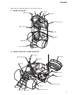
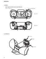
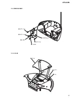
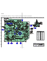
6-2. CIRCUIT BOARDS LOCATION
6-1. IC PIN DESCRIPTION
• IC802 uPD789477GC-A26-8BT (SYSTEM CONTROLLER)
Pin No.
Pin Name
I/O
Pin Description
1, 2
NC
—
Not used. (Open)
3 to 5
VLC2 to 0
I
LCD drive bias voltage input
6 to 9
COM0 to 3
O
LCD drive common output
10 to 26
S0 to 16
O
LCD drive segment output
27
REC
I
Tape record signal input H: REC
28
AC-CHK
I
AC power supply detection signal input L: AC in
29
CD-DOOR
I
CD door open/close switch input L: Close
30
S-ROCK
O
ROCK LED control signal output Not used. (Open)
31
S-POP
O
POP LED control signal output Not used. (Open)
32
S-JAZZ
O
JAZZ LED control signal output Not used. (Open)
33
S-VOCAL
O
VOCAL LED control signal output Not used. (Open)
34
LINE IN
O
LINE IN control signal output
35
A-MUTE
O
Audio mute output H: Mute
36
CD
O
CD function output H: CD
37
TAPE
O
Tape function output H: Tape
38
AVDD
—
Analog power supply pin for A/D converter (+3.3 V)
39
BTT-CHK-H
I
Battery check input for Hi-voltage
40
BTT-CHK-M
I
Battery check input for Mid-voltage
41
V CHECK
I
Voltage check input Not used. (Open)
42 to 45
KEY4 to 1
I
Key input
46
MODE CHK
I
Destination setting input
47
AGND
—
Analog ground for A/D converter
48
REMOTE
I
Sircs receiver data input
49
TC-PLAY
I
Tape play switch input L: Play
50
WP/INI
O
Wake-up/Initial setting read signal output
51
3.3V MONITOR
I
3.3V MONITOR signal input
52
C-WRQ
I
CD write request data input
53
C-DOUT
I
CD digital signal processor data input
54
C-DIN
O
CD digital signal processor data output
55
C-CLK
I
CD serial data transfer clock signal input
56
R-COUNT
I
Tuner PLL IF count input
57
R-DATA
O
Tuner PLL data output
58
R-CLK
O
Tuner PLL clock output
59
R-LAT
O
Tuner PLL latch output
60
B-MUTE
O
Tuner mute signal output H: Mute
61
C-DRF
I
CD DRF signal input
62
C-CE
O
CD chip enable output
63
C-FSEQ
I
CD frame SYNC input
64
C-XRT
O
CD system reset output
65
P-CON
O
System power control output H: PCON
66
ISS1
O
ISS1 output
67
ISS2
O
ISS2 output
68
DBB
O
MEGA BASS control output H: MEGA BASS off, L: MEGA BASS on
69
ICO
I
Connected to VSS.
70
XT1
I
Sub system oscillation input (32.768 kHz)
71
XT2
O
Sub system oscillation output (32.768 kHz)
72
VDD
—
Main power supply pin for A/D converter (+3.3 V)
73
VSS
—
Main ground
74
X1
I
Main system oscillation input (4.19 MHz)
75
X2
O
Main system oscillation output (4.19 MHz)
76
RST
I
System reset input
77
V-CLK
O
Volume clock output
78
V-DATA
O
Volume data output
79
SCL
O
EEPROM clock output
80
SDA
I/O
EEPROM input/output
TEN KEY board
TUNER board
TC board
BATTERY (1) board
BATTERY (2) board
MAIN board
LCD board
FUNCTION KEY board
HEADPHONE board
POWER board
POWER KEY board
VOL board
CD BUTTON board
CD board
Summary of Contents for CFD-S250 - Cd Radio Cassette-corder
Page 52: ...52 CFD S250 MEMO ...
Page 55: ...3 CFD S250 MEMO ...

