background image

CDP-XE270/XE370

REVISION  HISTORY

Clicking the version allows you to jump to the revised page.
Also, clicking the version at the upper right on the revised page allows you to jump to the next revised
page.

Ver.

Date

Description of Revision

1.0

2001.03

New

1.1

2001.07

Addition of Electrical Checks

1.2

2002.04

Addition of Silver type (CDP-XE370 AEP model)

(ENG-02006)

1.3

2006.02

Addition of Silver (Hair-line Finish) type (AEP, UK models)

(SPM-06013)

1.4

2006.07

Change of OPTICAL PICK-UP (PXR-104X

t

KSS-213C), and

Change of BD board (Suffix-12) according to it (Supplement-1)

(ECN-ECB51248)

Summary of Contents for CDP-XE270 - Compact Disc Player

Page 1: ...ion 11 W Dimensions approx 430 x 95 x 290 mm w h d incl projecting parts Mass approx CDP XE370 3 2 kg CDP XE270 3 2 kg Supplied accessories Audio cord 2 phono plugs 2 phono plugs 1 Remote commander remote 1 CDP XE370 only R6 size AA batteries 2 CDP XE370 only Design and specifications are subject to change without notice Load impedance Over 10 kilohms Wave length 660 nm Jack type Phono jacks Optic...

Page 2: ...s 13 6 2 Printed Wiring Board BD Board 14 6 3 Schematic Diagram BD Board 15 6 4 Printed Wiring Boards LOADING MAIN POWER SW Boards 16 6 5 Schematic Diagram LOADING MAIN POWER SW Boards 17 6 6 Printed Wiring Boards DISPLAY KEY Boards 18 6 7 Schematic Diagram DISPLAY KEY Boards 19 6 8 IC Pin Function Description 22 7 EXPLODED VIEWS 7 1 Case Section 26 7 2 Front Panel Section 27 7 3 CD Mechanism Deck...

Page 3: ...ions to use these instruments 2 A battery operated AC milliammeter The Data Precision 245 digital multimeter is suitable for this job 3 Measuring the voltage drop across a resistor by means of a VOM or battery operated AC voltmeter The limit indica tion is 0 75 V so analog meters must have an accurate low voltage scale The Simpson 250 and Sanwa SH 63Trd are ex amples of a passive VOM that is suita...

Page 4: ...ntrated so as to be focused on the disc reflective surface by the objective lens in the optical pick up block Therefore when checking the laser diode emis sion observe from more than 30 cm away from the objective lens LASER DIODE AND FOCUS SEARCH OPERATION CHECK Carry out the S curve check in CD section adjustment and check that the S curve waveforms is output three times MODEL IDENTIFICATION Rear...

Page 5: ... H 8 9 11 12 14 X 9 9 14 x 0 9 14 lAMSL dial qa 9 12 14 m M qk 9 13 LOCATION OF CONTROLS FRONT PANEL REMOTE CONTROL CDP XE370 only ANALOG OUT LEVEL qk 7 9 CHECK qg 12 CLEAR qf 12 CONTINUE 2 9 14 DISPLAY ON OFF qs 11 FADER qd 13 Number buttons 4 9 12 PROGRAM qa 9 REPEAT 6 9 SHUFFLE 1 9 TIME 3 10 BUTTON DESCRIPTIONS 10 5 9 12 N qh 9 11 12 14 X 8 9 14 x qj 9 14 AMS 9 9 12 14 m M 0 9 13 REAR PANEL ANA...

Page 6: ...FLOW SECTION 3 DISASSEMBLY Note Follow the disassembly procedure in the numerical order given 3 2 CASE 3 2 CASE Page 6 3 3 CD MECHANISM DECK CDM66 5BD27 Page 7 3 5 BASE UNIT BU 5BD27 Page 8 3 4 MAIN BOARD Page 7 SET 1 two screws case 3 TP2 1 two screws case 3 TP2 1 screw case 3 TP2 2 case ...

Page 7: ...1 8 CD mechanism deck CDM66 5BD27 BOTTOM VIEW 5 three screws BVTP3 8 6 Note When the power supply does not turn on rotate the cam with tepering driver 3 mm as the figure shows and the loading panel will be moved 1 connector CN602 2 wire flat type 17core CN621 2 wire flat type 21core CN651 5 main board 3 four screws BVTP3 8 4 two screws BVTP3 8 ...

Page 8: ...8 CDP XE270 XE370 3 5 BASE UNIT BU 5BD27 1 screw DIA 12 froating 3 three screws DIA 12 froating 4 holder 66 2 BOTTOM VIEW 5 two springs 932 compression 5 two springs 932 compression 6 base unit BU 5BD27 ...

Page 9: ...n OFF the power 7 Open circuit the test TP ADJ of the DISPLAY board and ground with a lead wire AFADJ MODE KEY AND FLUORESCENT INDICA TOR TUBE DISPLAY CHECK MODE Procedure 1 Short circuit the test TP AFADJ of the DISPLAY board and ground with a lead wire 2 Press the POWER button to turn ON the power The whole fluorescent indicator tube lights up 3 All buttons have individual button numbers When a ...

Page 10: ...10 CDP XE270 XE370 Checking Location DISPLAY BOARD Conductor Side TP ADJ TP AFADJ GND ...

Page 11: ... 12 RFDC Level Check Connection BD board TP FE1 TP VC oscilloscope A B symmetry within 2 1 Vp p BD board TP RFDC TP VC oscilloscope VOLT DIV 200 mV TIME DIV 500 ns level 1 15 0 35 Vp p VC Procedure 1 Connect an oscilloscope to test point TP RFDC and TP VC on the BD board 2 Turn the power on and insert the disc PATD 012 3 Turn the power off and enter the ADJ mode Refer to 4 Test Mode 4 Turn the pow...

Page 12: ...C voltage of the center of the Traverse waveform Confirm the following A B x 100 less than 22 Traverse Waveform 6 Press the TIME button The tracking servo and sledding servo are turned ON Confirm the C DC voltage is almost equal to the A DC voltage is step 5 Traverse Waveform Checking Location BD board BD board TP TE1 TP VC oscilloscope 0V B level 1 15 0 5 Vp p Center of the waveform A DC voltage ...

Page 13: ...trolytics and tantalums All resistors are in Ω and 1 4 W or less unless otherwise specified C panel designation A B Line B B Line Voltages and waveforms are dc with respect to ground under no signal conditions no mark CD PLAY Voltages are taken with aVOM Input impedance 10 MΩ Voltage variations may be noted due to normal produc tion tolerances Waveforms are taken with a oscilloscope Voltage variat...

Page 14: ...1 SPINDLE M102 SLED S101 LIMIT IC150 CN101 C136 C184 RB101 C124 RB102 IC131 CN102 R135 C145 R141 R172 R183 R182 C139 C174 C173 R171 R144 IC101 R191 R155 R145 R173 C183 R181 R127 R123 C123 C125 C120 R120 R122 C126 C122 R125 R129 R126 R121 C121 R153 R139 1 681 001 11 11 BD BOARD COMPONENT SIDE TP VC TP TE1 TP FE1 TP RFAC 1 681 001 11 11 M BD BOARD CONDUCTOR SIDE A MAIN BOARD CN651 M OPTICAL PICK UP ...

Page 15: ...15 15 CDP XE270 XE370 6 3 SCHEMATIC DIAGRAM BD Board See page 20 for Waveforms See page 20 for IC Block Diagrams Page 17 TP RFDC Ver 1 1 2001 07 ...

Page 16: ...JW629 JW605 C606 JW654 R647 CN621 C612 JW612 JW607 Q642 R631 Q692 JW673 R611 D605 JW614 C618 R806 C675 R904 R804 IC801 JW627 JW661 JW663 C641 JW638 C908 R641 R691 Q682 R692 R909 CN651 R812 C654 D613 JW604 JW618 R910 C609 JW603 R906 D604 D601 R646 T601 POWER TRANSFORMER D603 R681 NO603 JW613 R912 JW666 JW658 C677 R632 C608 JW611 D641 D602 IC651 JW616 NO631 C657 Q691 JW657 C605 R612 C604 C653 Q681 J...

Page 17: ...17 17 CDP XE270 XE370 6 5 SCHEMATIC DIAGRAM LOADING MAIN POWER SW Boards See page 20 for IC Block Diagram Page 15 Page 19 ...

Page 18: ...TP ADJ GND TP AFADJ DISPLAY BOARD l AMS L PUSH ENTER J681 B MAIN BOARD CN621 x S524 X S523 M S527 m S526 m S522 A OPEN CLOSE S521 IC501 E 1 2 4 32 34 35 FL501 FLUORESCENT INDICATOR TUBE 2 1 1 3 1 681 129 11 11 4 5 3 1 1 2 TIME PLAY MODE CLEAR REPEAT KEY BOARD 11 11 1 681 130 S501 504 S521 524 S526 527 A B C D E F 1 2 3 4 5 6 7 8 9 10 11 12 6 6 PRINTED WIRING BOARDS DISPLAY KEY Boards See page 13 f...

Page 19: ...19 19 CDP XE270 XE370 6 7 SCHEMATIC DIAGRAM DISPLAY KEY Boards See page 20 for Waveform Page 17 ...

Page 20: ... 80 4 XRST 3 SQCK SQSO 5 9 8 7 6 56 60 53 54 55 59 57 58 51 52 48 49 50 47 44 45 46 43 41 42 XLAT CLOK SENS SYSM DATA XUGF XPCK GFS C2PO WFCK 10 11 12 13 14 15 16 17 18 19 20 21 22 23 24 25 26 32 33 30 31 36 37 34 35 39 40 38 28 27 29 SPOA ATSK SCLK VDD SCOR SPOB XLON XTAI XVDD EMPH AVDD1 AOUT1 AIN1 XTAO XVSS AIN2 AOUT2 AVDD2 RMUT LOUT2 LOUT1 BCK LRCK PCMD LMUT AVSS1 AVSS2 CPU INTERFACE SERVO AUTO...

Page 21: ...ROM DVC 3 A B C D B C A A A B C D B C D D 1 2 APC AMP 5 6 7 8 9 4 RFAC SUMMING AMP RW ROM APC OFF Hi Z RW ROM H L VOFST VC RW ROM 10 11 GM GM 18 17 16 B D A C 13 14 15 12 EQ IN LD PD GND A B C D AC SUM E F DVCC DVC RFAC SW DC OFST RFDCI RFDCO VC RFC VFC BST RFG VCC CEI CE TE BAL TE FEI FE MAIN Board IC631 BA6956AN 1 2 3 4 5 6 7 8 9 CONTROL LOGIC TSD VREF OUT2 OUT1 RNF VM VCC FIN GND RIN ...

Page 22: ...t to the system controller IC501 21 COUT I O Numbers of track counted signal input output terminal Not used open 22 MIRR I O Mirror signal input output terminal Not used open 23 DFCT I O Defect signal input output terminal Not used open 24 FOK I O Focus OK signal input output terminal Not used open 25 LOCK I O GFS is sampled by 460 Hz H when GFS is H Not used open 26 MDP O Spindle motor M101 servo...

Page 23: ...ace L R sampling clock signal 44 1 kHz output terminal Not used open 62 PCMD O D A interface serial data output terminal Not used open 63 BCK O D A interface bit clock signal 2 8224 MHz output terminal Not used open 64 EMPH O H is output when playback disc is emphasis on L is output when playback disc is emphasis off Not used open 65 XVDD Power supply terminal 5V crystal oscillator system 66 XTAI ...

Page 24: ...LOSE H X x M m keys input 27 NC O Not used open 28 ADJ AFADJ BD TEST I Setting terminal for the test mode L ADJ test mode M AFADJ test mode H BD test mode 29 IN OUT SW I Loading in detect switch S152 and loading out detect switch S151 input terminal L load in H load out 30 RST I System reset signal input from the reset signal generator IC603 L reset For several hundreds msec after the power supply...

Page 25: ...XE370 Pin No Pin Name I O Description 73 NC Connected to the 5V power supply 74 to 77 NC O Not used open 78 SCOR I Subcode sync S0 S1 detection signal input from the CXD2587Q IC101 79 80 NC I Connected to the ground ...

Page 26: ...32 141 12 PANEL LOADING BLACK 1 4 232 141 32 PANEL LOADING SILVER XE270 AEP UK XE370 AEP 1 4 232 141 41 PANEL LOADING SILVER Hair line Finish AEP UK 2 X 4953 448 1 FOOT ASSY 3 1 500 386 11 FILTER CLAMP FERRITE CORE 4 3 703 244 00 BUSHING 2104 CORD 5 4 954 051 51 HOLDER PC BOARD 06 1 696 845 11 CORD POWER AUS 06 1 777 071 43 CORD POWER AEP UK SP 06 1 783 531 32 CORD POWER US CND 7 1 823 359 11 WIRE...

Page 27: ...1 X 4953 554 5 PANEL ASSY FRONT BLACK XE270 US CND 51 X 4954 948 1 PANEL ASSY FRONT SILVER XE370 AEP 52 4 231 928 01 KNOB AMS BLACK 52 4 231 928 11 KNOB AMS SILVER XE270 AEP UK XE370 AEP 52 4 231 928 31 KNOB AMS SILVER for Hair line Finish AEP UK 53 4 231 973 01 BUTTON POWER BLACK 53 4 231 973 11 BUTTON POWER SILVER XE270 AEP UK XE370 AEP 53 4 231 973 51 BUTTON POWER SILVER for Hair line Finish AE...

Page 28: ... 505 4 232 713 01 BELT LD 506 4 232 711 01 GEAR LD 507 4 993 142 21 PULLEY L PRESS 508 1 452 925 21 MAGNET ASSY 509 4 231 529 05 CHASSIS 66 510 4 227 899 31 SCREW DIA 12 FROATING 513 1 645 721 11 LOADING BOARD 514 4 959 996 01 SPRING 932 COMPRESSION 515 4 231 531 01 HOLDER 66 M151 A 4604 363 A MOTOR L ASSY LOADING 2 7 621 775 10 SCREW B 2 6X4 510 515 514 513 514 510 M151 2 BU 5BD27 not supplied 50...

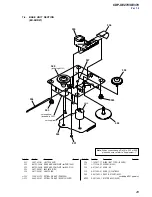
Page 29: ...0555 1 796 033 12 OPTICAL PICK UP PXR 104X 0555 8 848 483 21 OPTICAL PICK UP KSS 213C C2RP 556 1 782 817 11 WIRE FLAT TYPE 16 CORE 557 3 713 786 51 SCREW M2X3 558 4 917 567 01 GEAR M 559 4 917 564 01 GEAR P FLATNESS 560 X 4917 523 3 BASE OUTSERT ASSY including M101 spindle M102 X 4917 504 1 MOTOR ASSY SLED 556 555 557 558 553 559 551 552 553 560 554 M102 not supplied not supplied included in 560 i...

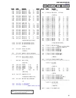
Page 30: ... parts so they may have some difference from the original one RESISTORS All resistors are in ohms METAL Metal film resistor METAL OXIDE Metal oxide film resistor F nonflammable Items marked are not stocked since they are seldom required for routine service Some delay should be anticipated when order ing these items SEMICONDUCTORS In each case u µ for example uA µA uPA µPA uPB µPB uPC µPC uPD µPD C...

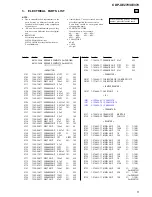
Page 31: ...L501 1 518 745 11 INDICATOR TUBE FLUORESCENT IC IC501 8 752 921 32 IC CXP82324 093Q IC561 8 759 459 86 IC NJL64H400A REMOTE CONTROL RECEIVER TRANSISTOR Q541 8 729 029 66 TRANSISTOR DTC114ESA RESISTOR R501 1 249 427 11 CARBON 6 8K 5 1 4W R511 1 249 427 11 CARBON 6 8K 5 1 4W R521 1 249 427 11 CARBON 6 8K 5 1 4W R522 1 249 415 11 CARBON 680 5 1 4W R523 1 249 417 11 CARBON 1K 5 1 4W R524 1 249 419 11 ...

Page 32: ...IODE 11ES2 NTA2B D604 8 719 024 99 DIODE 11ES2 NTA2B D605 8 719 024 99 DIODE 11ES2 NTA2B D612 8 719 210 21 DIODE 11EQS04 D613 8 719 210 21 DIODE 11EQS04 D614 8 719 947 13 DIODE MTZJ T 72 4 7B D615 8 719 911 19 DIODE 1SS119 25 D616 8 719 911 19 DIODE 1SS119 25 D631 8 719 983 63 DIODE MTZJ T 72 3 3B D641 8 719 983 84 DIODE MTZJ T 72 30D D643 8 719 109 85 DIODE RD5 1ESB2 D681 8 719 911 19 DIODE 1SS11...

Page 33: ... UK SP AUS XE370 58 1 773 041 11 WIRE FLAT TYPE 17 CORE 508 1 452 925 21 MAGNET ASSY 0555 1 796 033 12 OPTICAL PICK UP PXR 104X 0555 8 848 483 21 OPTICAL PICK UP KSS 213C C2RP 556 1 782 817 11 WIRE FLAT TYPE 16 CORE 560 X 4917 523 3 BASE OUTSERT ASSY including M101 spindle M102 X 4917 504 1 MOTOR ASSY SLED M151 A 4604 363 A MOTOR L ASSY LOADING 0T601 1 437 257 11 TRANSFORMER POWER US CND 0T601 1 4...

Page 34: ...34 CDP XE270 XE370 MEMO ...

Page 35: ...PICK UP PXR 104XtKSS 213C and Change of BD board Suffix 12 according to it CDP XE270 AEP UK Australian Singapore models CDP XE370 AEP UK models only 8 848 483 21 OPTICAL PICK UP KSS 213C C2RP Part No A 4725 568 B Printed of Silk 1 681 001 12 R135 1 216 833 11 METAL CHIP 10K 5 1 10W R136 1 216 833 11 METAL CHIP 10K 5 1 10W R139 1 216 848 11 METAL CHIP 180K 5 1 10W R141 1 216 838 11 METAL CHIP 27K 5...

Page 36: ... path J CD PLAY ANALOG OUT c CD PLAY DIGITAL OUT Note on Printed Wiring Board X parts extracted from the component side Y parts extracted from the conductor side Pattern from the side which enables seeing The other layers patterns are not indicated Caution Pattern face side Parts on the pattern face side seen from Conductor Side the pattern face are indicated Parts face side Parts on the parts fac...

Page 37: ...R102 C130 C137 E E M101 SPINDLE M102 SLED S101 LIMIT IC150 CN101 C136 C184 RB101 C124 RB102 IC131 CN102 R135 C145 R141 R172 R183 R182 C139 C174 C173 R171 R144 IC101 R191 R155 R145 R173 C183 R181 R127 R123 C123 C125 C120 R120 R122 C126 C122 R125 R129 R126 R121 C121 R153 R139 TP DGND 1 681 001 12 12 BD BOARD COMPONENT SIDE TP VC TP TE1 TP FE1 TP RFAC 1 681 001 12 12 M BD BOARD CONDUCTOR SIDE A MAIN ...

Page 38: ...70 TP RFDC Refer to page 17 on service manual R135 136 10k FOR KSS 213C 22k FOR PXR 104X 120k FOR PXR 104X 180k FOR KSS 213C R145 5 6k FOR PXR 104X 7 5k FOR KSS 213C R141 27k FOR KSS 213C 39k FOR PXR 104X 2 2 SCHEMATIC DIAGRAM BD Board ...

Page 39: ...126 205 11 ELECT CHIP 47uF 20 6 3V 3 ELECTRICAL PARTS LIST NOTE Due to standardization replacements in the parts list may be different from the parts specified in the diagrams or the components used on the set XX and X mean standardized parts so they may have some difference from the original one RESISTORS All resistors are in ohms METAL Metal film resistor METAL OXIDE Metal oxide film resistor F ...

Page 40: ...5K 5 1 10W for KSS 213C R146 1 216 845 11 METAL CHIP 100K 5 1 10W R149 1 216 821 11 METAL CHIP 1K 5 1 10W R151 1 216 845 11 METAL CHIP 100K 5 1 10W R152 1 216 833 11 METAL CHIP 10K 5 1 10W R153 1 216 864 11 SHORT CHIP 0 R155 1 216 837 11 METAL CHIP 22K 5 1 10W R171 1 218 720 11 METAL CHIP 15K 0 5 1 10W R172 1 218 720 11 METAL CHIP 15K 0 5 1 10W R173 1 218 720 11 METAL CHIP 15K 0 5 1 10W R174 1 216...

Page 41: ...7 CDP XE270 XE370 MEMO ...

Page 42: ...e next revised page Ver Date Description of Revision 1 0 2001 03 New 1 1 2001 07 Addition of Electrical Checks 1 2 2002 04 Addition of Silver type CDP XE370 AEP model ENG 02006 1 3 2006 02 Addition of Silver Hair line Finish type AEP UK models SPM 06013 1 4 2006 07 Change of OPTICAL PICK UP PXR 104XtKSS 213C and Change of BD board Suffix 12 according to it Supplement 1 ECN ECB51248 ...

Reviews: