


CDP-XB630
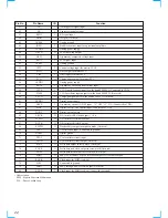
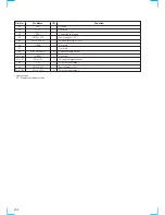
13
13
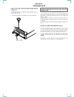
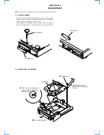
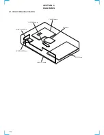
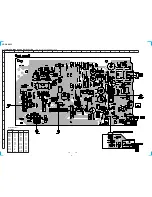
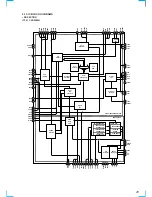
6-3. PRINTED WIRING BOARD LOADING MOTOR SECTION
• See page 12 for Circuit Board Location.
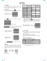
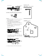
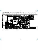
6-2. SCHEMATIC DIAGRAM LOADING MOTOR SECTION
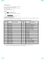
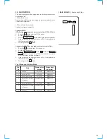
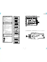
THIS NOTE IS COMMON FOR PRINTED WIRING
BOARDS AND SCHEMATIC DIAGRAMS.
(In addition to this, the necessary note is printed
in each block.)
For schematic diagrams.
Note:
• All capacitors are in µF unless otherwise noted. pF: µµF
50 WV or less are not indicated except for electrolytics
and tantalums.
• All resistors are in
Ω
and
1
/
4
W or less unless otherwise
specified.
•
¢
: internal component.
•
C
: panel designation.
•
U
: B+ Line.
•
V
: B– Line.
• Voltages and waveforms are dc with respect to ground
under no-signal (detuned) conditions.
no mark : STOP
(
) : PLAY
• Voltages are taken with a VOM (Input impedance 10 M
Ω
).
Voltage variations may be noted due to normal produc-
tion tolerances.
• Waveforms are taken with a oscilloscope.
Voltage variations may be noted due to normal produc-
tion tolerances.
• Circled numbers refer to waveforms.
• Signal path.
J
: CD
c
: digital out
For printed wiring boards.
Note:
•
X
: parts extracted from the component side.
•
Y
: parts extracted from the conductor side.
•
p
: parts mounted on the conductor side.
•
®
: Through hole.
•
b
: Pattern from the side which enables seeing.
(The other layers' patterns are not indicated.)
• Waveforms
Caution:
Pattern face side: Parts on the pattern face side seen from the
(Side B)
pattern face are indicated.
Parts face side:
Parts on the parts face side seen from the
(Side A)
parts face are indicated.
• Indication of transistor
C
These are omitted
E
B
Q
C
These are omitted
E
B
Note: The components identified by mark
!
or dotted line
with mark
!
are critical for safety.
Replace only with part number specified.
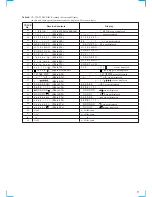
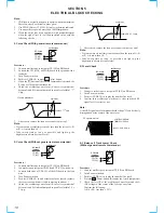
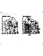
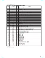
3.9Vp-p
16.93MHz
1.2Vp-p
(PLAY)
2.5V
APPROX 500mVp-p (PLAY)
2.5V
APPROX 200m Vp-p (PLAY)
7.5
µ
sec
2.4Vp-p
4.9Vp-p
16.93MHz
5Vp-p
2.1MHz
4.5Vp-p
33.8MHz
3.7Vp-p
8MHz
1
IC101
&¡
XTAI
2
IC101
%º
RF AC
3
IC101
$¡
TE
4
IC101
#ª
FE
5
IC101
@∞
MDP
6
IC661
6
384FS
7
IC661
0
BCK
8
IC661
@¡
XOUT
9
IC501
#ª
EXTAL
(Page 17)
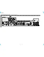
11
(21)
S152
LOAD
IN
S151
LOAD
OUT
CN151
1
5
M151
LOADING
MOTOR
M
LOADING BOARD
1 - 6 4 5 - 7 2 1 -
(Page 16)


