Skylab M&C Technology Co., Ltd.
WG203-User Manual
WG203-UM-001,A/1
4
12
GND
G
Ground
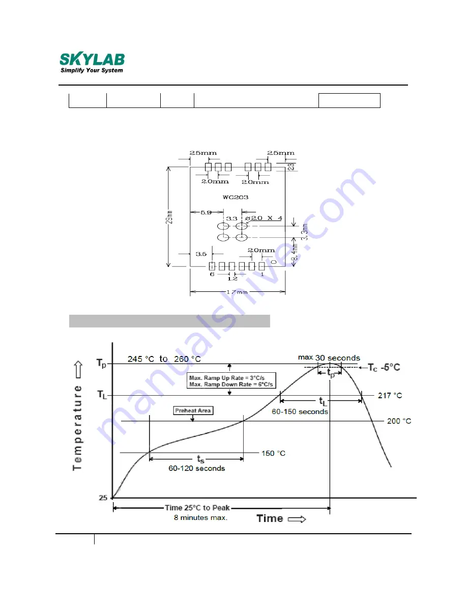
PCB Footprint and Dimensions
Figure 4: WG203 Footprint
Manufacturing Process Recommendations
Page 1: ...upporting 130Mbps for 20MHz and 300Mbps for 40MHz channel and IEEE 802 11b g data rates It supports two transmit traffic stream and two receive traffic stream using two Tx chain and two receive chain...
Page 2: ...Windows 7 32 64bit Linux Android MIMO power save Data rates of up to 54 Mbps for 802 11g and 144 4 for 802 11n HT20 300 Mbps for HT40 RoHS compliance meets environment friendly requirement 29 L x 17 W...
Page 3: ...age Pin Description Pin No Pin name I O Description Remark 1 1 5V P Module Power Supply 2 GND G Ground 3 3 3V P Module Power Supply 4 USB_D I O USB Interface DM 5 USB_D I O USB Interface DP 6 GND G Gr...
Page 4: ...Skylab M C Technology Co Ltd WG203 User Manual WG203 UM 001 A 1 4 12 GND G Ground PCB Footprint and Dimensions Figure 4 WG203 Footprint Manufacturing Process Recommendations...
Page 5: ...perties of the baseboard etc Exceeding the maximum soldering temperature in the recommended soldering profile may permanently damage the module Packaging Specification Figure 6 WG203 Packaging WARNING...
Page 6: ...iver is connected This device complies with part 15 of the FCC rules Operation is subject to the following two conditions 1 this device may not cause harmful interference and 2 this device must accept...
Page 7: ...at may cause undesired operation 2 Changes or modifications not expressly approved by the party responsible for compliance could void the user s authority to operate the equipment The devices must be...