Skylab M&C Technology Co., Ltd.
SKW17- User Manual
5
SKW17-
U
M
-
001
,A/0
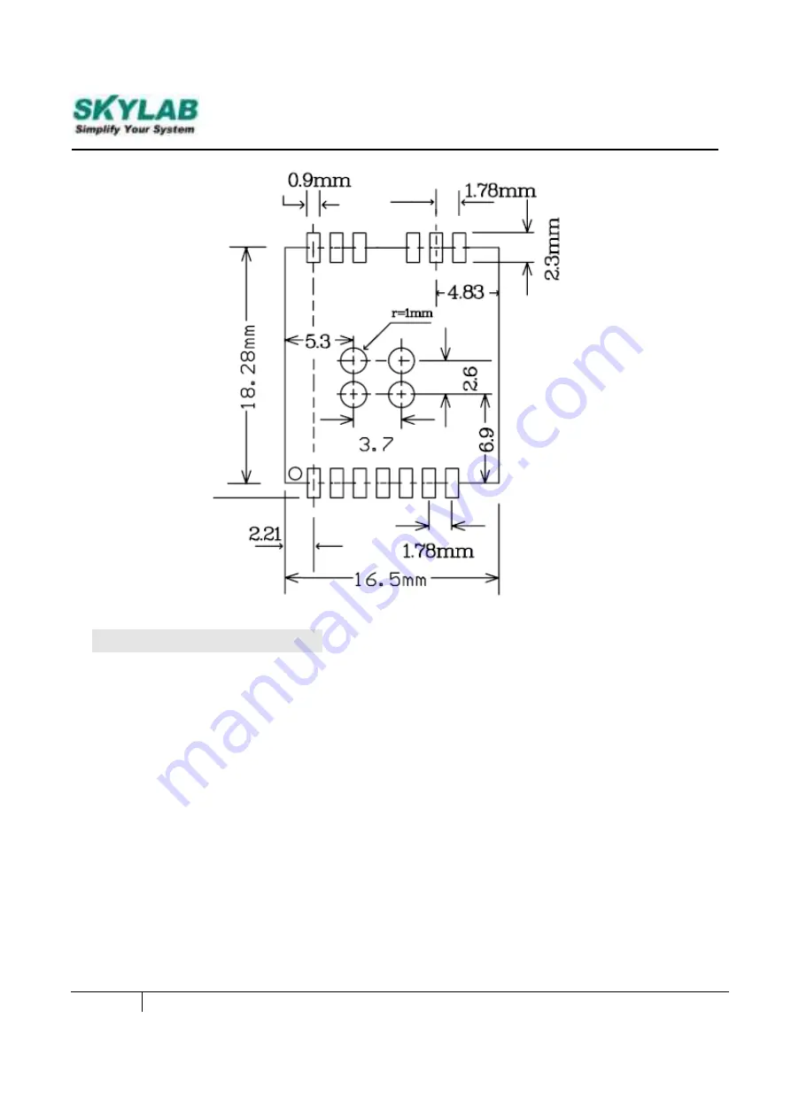
Figure 4: SKW17 Footprint
Reference design schematic
Page 1: ...run more of the WiFi function on chip The integrated CPU offloads the wireless processing overhead from the host appliance and enables consumer electronic devices to support WiFi functions seamlessly...
Page 2: ...ets environment friendly requirement 18 5 L x 16 6 W x 2 75 H mm small dimension Applications Block Diagram Figure 1 SKW17 Block Diagram Ordering Information Module NO RF Connector Type Antenna Option...
Page 3: ...gy Co Ltd SKW17 User Manual 3 SKW17 UM 001 A 0 Module Pinout Figure 2 SKW17 Pin Package Pin Description Pin No Pin name I O Description Remark 1 LED O Light Emitting Diode Driver up to 24mA 2 USB_D I...
Page 4: ...Ground 5 VDD_3V3 P Module Power Supply 6 GND G Ground 7 WPS I Wi Fi Protected Setup 250 K PU 8 GND G Ground 9 GND G Ground 10 GND G Ground 11 GND G Ground 12 RF RF port Antenna For SKW17A IPEX RF RF...
Page 5: ...Skylab M C Technology Co Ltd SKW17 User Manual 5 SKW17 UM 001 A 0 Figure 4 SKW17 Footprint Reference design schematic...
Page 6: ...Skylab M C Technology Co Ltd SKW17 User Manual 6 SKW17 UM 001 A 0 Figure 5 SKW17 Typical Reference design schematic...
Page 7: ...ication Figure 6 SKW17 Packaging Skylab M C Technology Co Ltd Address 9th Floor Zhongguang Building Yayuan Road Bantian Shenzhen Phone 86 755 8340 8210 Sales Support Phone 86 755 8340 8510 Technical S...
Page 8: ...rference and 2 this device must accept any interference received including interference that may cause undesired operation RF Exposure Compliance This equipment complies with FCC radiation exposure li...
Page 9: ...e used in all EU member states Use the WIFI Module in the environment with the temperature between 0 and 70 Operation Frequency 2412MHz 2472MHz 802 11b 802 11g 802 11n HT20 Max output power 0 0813W Ma...
Page 10: ...9 SKW17 UM 001 A 0 Skylab M C Technology Co Ltd SKW17 User Manual...