background image


SiRFatlasV 

Hardware Design Guide 


January, 2010 

SiRF Design Guide 

– Proprietary and Confidential 

               10


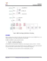
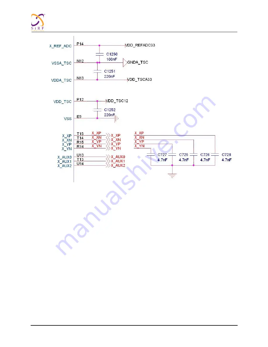
Figure 4: ADC Power Supply and Reference Decoupling 

SD/MMC 

Add  an  external  pull-up  resistor  to  all  data  and  command  signals  when  using  an  SD/MMC  card  or  an 
iNAND/moviNAND card. 

Use SD0 but not SD2 as the boot media. 

For MMC/ moviNAND, the pull-up resistor should be: 


50 kOhm ~ 100 kOhm for the DATA net 


4.7 kOhm ~ 100 kOhm for the CMD net 

For SD/iNAND, the pull-up resistors to all data and command signals should be 10 kOhm ~ 100 kOhm. 

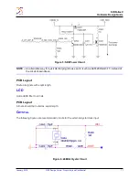
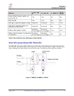
Add a quick discharging circuit by pulling the SD0's power low to GND with a 1 kOhm resistor when SD0 
is in power-down state (see R307 to Q303 in Figure 5

.) The reason for doing this is: 


The iNAND may not reboot normally if it did not discharge after power-off.  


Summary of Contents for SiRFatlasV

Page 1: ...er CS 129512 UG Issue 3 INTRODUCTION This document serves as a hardware design guide for the SiRFatlasV SoC based Evaluation Board EVB including boot configuration power supply and peripheral interfaces such as RAM ROM USB and more For details about theschematics contact SiRF field application engineers FAE ...

Page 2: ...play Graphics and Multimedia 1 Peripherals and Interfaces 1 Power Integration 1 Audio Integration 1 NAND Flash Storage 2 SD MMC MMC Controller 2 USB Connectivity 2 Packaging 2 Temperature Range 2 SiRFatlasV System Block Diagram 3 Boot Configuration 4 Power Supply 5 Power Pins 5 Decoupling CAP and Placement on the PCB Board 6 Power Consumption 6 Power On Sequence 6 On Chip PMU 6 Modac 7 UART 7 I2 C...

Page 3: ...nd Confidential ii USB 8 PCB Layout 8 TSC ADC 9 Add ESD devices to the Touch Screen Interface TSI for ESD protection 9 PCB Layout 9 SD MMC 10 PCB Layout 11 LCD 11 PCB Layout 11 Crystal 11 PCB Layout 12 GPIO 12 Reset Button Connection 12 Avoid I O Leakage During SoC Power Off 14 ...

Page 4: ...Behavior when Working as a Reset Button 14 List of Figures Figure 1 SiRFatlasV System Block Diagram 3 Figure 2 USB DP DN Route 8 Figure 3 USB Layout Rule 9 Figure 4 ADC Power Supply and Reference Decoupling 10 Figure 5 SD0 Power Circuit 11 Figure 6 24MHz Crystal Circuit 11 Figure 7 32 768KHz Crystal Circuit 12 Figure 8 P MOS and N MOS in I OPad 14 Figure 9 Random RTC Reset or On Key 15s Issue 15 F...

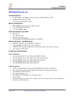
Page 5: ... I F TFT LCD panel Hardware VPP Video post processor for de interlace scalar color space conversion Two hardware overlay layers Peripherals and Interfaces Power Integration Two switching DC DC for core 700mA and DRAM 500mA One high PSRR and low noise 150mA LDO for I O and peripheral One high PSRR and low noise 100mA LDO for analog power One high PSRR and low noise 10mA LDO for PLL One high PSRR an...

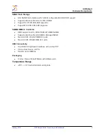
Page 6: ... pagesize Support MLC 2KB 4KB 8KB page size SD MMC MMC Controller SDIO support for WiFi DVB T DVB H T DMB S DMB Supports direct boot from SD MMC Managed NAND Two 8 bit SD1 01 SD 2 1 MMC4 3 ports Two 4 bit SD1 01 SD2 1 MMC4 3 ports USB Connectivity One USB 2 0 High Speed interfaces with on chipPHY Can be Host Device or OTG Transfer up to 480Mbps Packaging 10mm x 13mm 285 ball TFBGA with 0 65mm pitc...

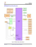
Page 7: ...SiRFatlasV Hardware Design Guide January 2010 SiRF Design Guide Proprietary and Confidential 3 SiRFatlasV SYSTEM BLOCK DIAGRAM Figure 1 SiRFatlasV System Block Diagram ...

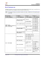
Page 8: ...2 B00 Normal 2 B01 Normal With ARM JTAG 2 B10 Function ATE 2 B00 Embedded ROM NAND Boot SLC 1 b0 SLC 1 b0 2KB page 1 b1 4KB page 1 b1 LBA Nand 1 bx 2KB page 2 B01 NAND Boot SLC 1 bx Don t Care 1 b0 512B page 1 b1 2KB page 2 B10 Embedded ROM NAND Boot MLC 1 b0 ECC 12bit per 1KB 1 b0 2KB page 1 b1 4KB page 1 b1 ECC 24bit per 1KB 1 b0 4KB page 1 b1 8KB page 2 B11 Embedded ROM SD MMC Boot 2 B11 TEST M...

Page 9: ...ust be used as the debug port for the MLC SD boot mode POWER SUPPLY Power Pins Pin Name Typical Voltage V Description VDDIO_L 3 3 3 0 2 8 1 8 LCD related I O pads power VDDIO_N 3 3 3 0 2 8 1 8 NAND flash related I O pads power VDDIO 3 3 3 0 2 8 I O pads power VDDIO_MEM 1 8 2 5 The pad power of the memory interface VDD_CORE 1 2 Main core digital power GND Main digital GND VDDIO_RTC 3 3 RTC pad powe...

Page 10: ... for the sample PCB layout Power Consumption For power andcurrent budget refer to CS 130805 DS SiRFatlasV Datasheet Power On Sequence The SiRFatlasV system power on sequence should follow the sequence in the CS 130805 DS SiRFatlasV Datasheet The power on reset has two important valid reset time values RTC power on reset X_RTC_RST_B should keep the logic low after the 32KHz crystal is stable SOC lo...

Page 11: ...LDO5 3 3V VDDIO_RTC Table 3 On Chip PMU Specificationsand Applications MODAC Refer to CS 130255 UG SiRFatlasV Audio Hardware Design Guide for the Modac design UART There are two UARTs on the SiRFatlasV chip but only UART0 has the DMA function Use UART0 to transmit large amounts of data at high speed UART0 has a hardware flow control function UART1 must be used as the debug port I2 C Add pull up re...

Page 12: ...istor in series with the pin x_usb_vbus to prevent overvoltage PCB Layout The USB 2 0 specification requires that the USB DP DN traces maintain a 90 Ohm differential impedance see paragraph 7 1 1 3 in USB specification Rev 2 0 for more details A continuous ground plane is required directly beneath the DP DN traces and extending at least 5 times the spacing width to either side of the DP DN lines M...

Page 13: ...ording to the following rules Keep all analog net routing as small as possible Shield all critical analog nets using the Analog Ground AGND especially single ended nets Pay attention to the routing of the input lines Any noisecoupling will be treated as an input signal thereby reducing the dynamic range of the ADC Keep all analog reference and power supply lines as wide as possible Respect the max...

Page 14: ... SD2 as the boot media For MMC moviNAND the pull up resistor should be 50 kOhm 100 kOhm for the DATA net 4 7 kOhm 100 kOhm for the CMD net For SD iNAND the pull up resistors to all data and commandsignals should be 10 kOhm 100 kOhm Add a quick discharging circuit by pulling the SD0 s power low to GND with a 1 kOhm resistor when SD0 is in power down state see R307to Q303 in Figure 5 The reason for ...

Page 15: ...r quick discharging is to use an IC such as AAT4280IGU 3 T1 instead of the circuit shown above PCB Layout Route all signals with equal length LCD Add anEMI filter to all nets PCB Layout All nets should be routed as equal length CRYSTAL The following figures are recommendedcircuits for the external crystal clock input Figure 6 24MHz Crystal Circuit ...

Page 16: ...uring running mode for better powerconsumption management RESET BUTTON CONNECTION SiRFatlasV has several reset function pins X_RTC_RST_B This is a reset signal used to reset all RTC domain logic and power on off control logic After the VDDIO_RTC first powers on X_RTC_RST_B should be active to guarantee that the RTC logic is reset and the power on off control logic enters the RTC_COLDBOOT state Whe...

Page 17: ...es No SYSRTC Yes Yes No No RISC Core Power off Power off Yes Yes RISC Interface Power off Power off Yes Yes Interrupt Controller Power off Power off Yes Yes CLKC Power off Power off Yes Yes Timer Power off Power off Yes Yes Reset controller Power off Power off Yes No GPIO Power off Power off Yes Yes System Arbiter Power off Power off Yes Yes RISC CP14 Registers Power off Power off Yes No Other SoC...

Page 18: ...whensystem is running No press On_key again No press On_key again Yes Yes Reboot when thesystem is in deep sleep or hibernation No press On_key again No press On_key again No No Table 5 Reset Behavior when Working asa Reset Button AVOID I O LEAKAGE DURING SOC POWER OFF The SiRFatlasV SoC has an ESD protection circuit between the I O pad s power and the I O pad when the I O pad is not powered there...

Page 19: ...e RF chip keeps driving signals to to the SoC s I O pad through the GPS BB signal pads and the pad s internal ESD circuit leakage will go to the I O VDD Although the I O LDO is disabled this leakage causes the I O VDD to have a 1 xV 2 xV floating voltage therefore the RF LDO s enable signal and LCD backlight boost s enable signal will also have a 1 xV 2 xV level signal The voltage may be above the...

Page 20: ...n disable status at the default reset stage NOTE RC delay of X_RESET_B is about 20ms and RC delay of X_RTC_RST_B is about 880ms System is in deep sleep or hibernation mode with peripheral power on and drive signal to SoC When the system goes into deep sleep or hibernation mode x_system_en is pulled low and most of the SoC s power is disabled However there is still a chance that some external modul...

Page 21: ...17 Insert aswitch on the signal path between the powered external module and theSoC I O pads Use the SoC s I O to control the switch or control the external module s power supply to makesure that when system goes into deep sleep or hibernationmode the external module is powered off at same time ...

Page 22: ... from the use of integrated circuits based on this document including but not limited to claims or damages based on infringement of paten ts copyrights or other intellectual property rights SiRF makes no warranties either express or implied with respect to the information and specifications contained in this document Performance characteristics listed in this data sheet do not constitute a warrant...

Reviews: