background image


                                                                                                                                          Smart Machine Smart Decision


SIM2000S_Hardware_Design_V1.00

                                            52                       

                          2014-02-27


II.


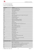
Terms and Abbreviations 

Table 51: Terms and abbreviations 

Abbreviation  

Description 

CDMA 

Code Division Multiple Access   

RUIM 

Removable User Identity Module 

ADC  

Analog-to-Digital Converter 

CS  

Coding Scheme 

CSD  

Circuit Switched Data 

CTS  

Clear to Send 

DTE  

Data Terminal Equipment (typically computer, terminal, printer) 

DTR  

Data Terminal Ready 

DTX  

Discontinuous Transmission 

ESD  

Electrostatic Discharge 

ETS  

European Telecommunication Standard 

IMEI  

International Mobile Equipment Identity 

Li-ion 

Lithium-Ion 

MO  

Mobile Originated 

MS  

Mobile Station (CDMA engine), also referred to as TE 

MT  

Mobile Terminated 

PAP  

Password Authentication Protocol 

PBCCH  

Packet Broadcast Control Channel 

PCB  

Printed Circuit Board 

PDU  

Protocol Data Unit 

PPP  

Point-to-point protocol 

RF  

Radio Frequency 

RMS  

Root Mean Square (value) 

RX  

Receive Direction 

SMS  

Short Message Service 

TE  

Terminal Equipment, also referred to as DTE 

TX  

Transmit Direction 

UART 

Universal Asynchronous Receiver & Transmitter 

BC0 

The 800 MHz cellular band 

BC1 

The PCS band 

Phonebook abbreviations 

FD 

RUIM fix dialing phonebook 

LD  

RUIM last dialing phonebook (list of numbers most recently dialed) 

MC  

Mobile Equipment list of unanswered MT calls (missed calls) 

ON 

RUIM (or ME) own numbers (MSISDNs) list 

RC  

Mobile Equipment list of received calls 

SM  

RUIM phonebook 

Summary of Contents for SIMCom SIM2000S

Page 1: ...SIM2000S_Hardware_Design_V1 00 ...

Page 2: ... the customer s possession Furthermore system validation of this product designed by SIMCom within a larger electronic system remains the responsibility of the customer or the customer s system integrator All specifications supplied herein are subject to change Copyright This document contains proprietary technical information which is the property of SIMCom Limited copying of this document and gi...

Page 3: ...et Function 22 4 3 Power Saving Mode 23 4 3 1 Minimum Functionality Mode 23 4 3 2 Sleep Mode AT CSCLK 1 24 4 3 3 Wake Up SIM2000S from Sleep Mode AT CSCLK 1 24 4 4 Serial Port and Debug Interface 24 4 4 1 Function of Serial Port 25 4 4 2 Serial Interfaces 25 4 4 3 USB Interface 27 4 4 4 Software Upgrade and Debug 28 4 4 5 Multiplexing function of serial port and SD interface 28 4 5 RI behaviors 28...

Page 4: ...ntenna Interface 42 5 PCB Layout 44 5 1 Pin Assignment 44 5 2 Principle of PCB layout 45 5 2 1 Antenna Interface 45 5 2 2 Power Supply 45 5 2 3 RUIM Card Interface 45 5 2 4 Audio Interface 45 5 2 5 Others 45 6 Electrical Reliability and Radio Characteristics 46 6 1 Absolute Maximum Ratings 46 6 2 Recommended Operating Conditions 46 6 3 Digital Interface Characteristics 46 6 4 RUIM_VDD Characterist...

Page 5: ...DEFINITION 34 TABLE 20 PCM SPECIFICATION 35 TABLE 21 PCM MULTIPLEXING FUNCTION 35 TABLE 22 TIMING PARAMETERS 36 TABLE 23 TIMING PARAMETERS 37 TABLE 24 PIN DEFINITION OF THE KEYPAD INTERFACE 38 TABLE 25 KEYPAD MULTIPLEXING FUNCTION 39 TABLE 26 PIN DEFINITION OF THE I2 C 39 TABLE 27 I2C MULTIPLEXING FUNCTION 39 TABLE 28 PIN DEFINITION OF THE GPIO 40 TABLE 29 PIN DEFINITION OF THE ADC 40 TABLE 30 ADC...

Page 6: ...2014 02 27 TABLE 46 OPERATING FREQUENCIES 48 TABLE 47 CONDUCTED RECEIVE SENSITIVITY 48 TABLE 48 MOISTURE SENSITIVITY LEVELAND FLOOR LIFE 50 TABLE 49 BAKING REQUIREMENTS 50 TABLE 50 RELATED DOCUMENTS 51 TABLE 51 TERMS AND ABBREVIATIONS 52 TABLE 52 SAFETY CAUTION 53 ...

Page 7: ... 27 FIGURE 18 RI BEHAVIOUR OF VOICE CALLING AS A RECEIVER 29 FIGURE 19 RI BEHAVIOUR OF DATA CALLING AS A RECEIVER 29 FIGURE 20 RI BEHAVIOUR OF URC OR RECEIVE SMS 29 FIGURE 21 RI BEHAVIOUR AS A CALLER 30 FIGURE 22 SPEAKER REFERENCE CIRCUIT 30 FIGURE 23 MICROPHONE REFERENCE CIRCUIT 31 FIGURE 24 REFERENCE CIRCUIT OF THE 8 PIN RUIM CARD HOLDER 32 FIGURE 25 REFERENCE CIRCUIT OF THE 6 PIN RUIM CARD HOLD...

Page 8: ...Smart Machine Smart Decision SIM2000S_Hardware_Design_V1 00 8 2014 02 27 Version History Date Version Description of change Author 2014 02 27 1 00 draft Yanwu Wang Haibing Ye ...

Page 9: ...between the module and customers boards z One full modem serial port z One USB the USB interface can be used debug download software z One debug interface z Two ADC interface z Audio channel which includes a microphone input and a receiver output z Programmable general purpose input and output z A RUIM card interface z Support one PWM z I2C interface z The keypad interface 5 5 z PCM interface SIM2...

Page 10: ...eaks Debug port z Debug_TXD z Debug_RXD z USB_VBUS z USB_DM USB interface z USB_DP CDMA Protocol z IS95 A B Protocol Between MS BTS z IS 96A Voice Signal Coding z IS 98A Base MS Function z IS 126 Voice Loop Back z IS 637 Short Message Service z IS 707 Data Service z IS 657 Packet Data Phone book management Support phonebook types SM DC FD LD MC ME RC EN RUIM interface Support identity card 1 8V 3V...

Page 11: ...gs Normal operation CDMA 1X There is CDMA 1X data transfer in progress In this case power consumption is related with network settings uplink downlink data rates and CDMA 1X configuration Power down Normal power down by sending AT command AT CPOWD 1 or using the PWRKEY The power management unit shuts down the power supply for the baseband part of the module Software is not active The serial port i...

Page 12: ...Smart Machine Smart Decision Figure 1 SIM2000S functional diagram SIM2000S_Hardware_Design_V1 00 12 2014 02 27 ...

Page 13: ... Package Information 3 1 Pin out Diagram Figure 2 SIM2000S pin out diagram Top view 3 2 Pin Description Table 3 Pin description Pin name Pin number I O Power domain V Description Comment SIM2000S_Hardware_Design_V1 00 13 2014 02 27 ...

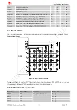
Page 14: ...sed keep open Status STATUS 66 O 2 85 Power on status NETLIGHT 52 O 1 8 Network status If these pins are unused keep open PCM interface PCMCLK 11 O PCMIN 12 I PCMOUT 13 O PCMSYNC 14 O 1 8 PCM interface If these pins are unused keep open USB interface VBUS 6 I 4 4 5 5 USB_DP 23 I O USB_DM 24 I O Debug and download If these pins are unused keep open I2 C interface SDA 37 I O I2C serial bus data SCL ...

Page 15: ... RUIM card Support 1 8V or 3V RUIM card RUIM_DATA 31 I O RUIM data input output RUIM_CLK 32 O RUIM clock RUIM_RST 33 O 1 8 3 RUIM reset All signals of RUIM interface should be protected against ESD with a TVS diode array RUIM_PRESENCE 34 I 1 8 RUIM card detection If it is unused keep open ADC ADC1 25 I Input voltage range 0V 2 5V ADC2 36 I Input voltage range 0V 2 5V If it is unused keep open Exte...

Page 16: ...Smart Machine Smart Decision 3 3 Package Dimensions Figure 3 Dimensions of SIM2000S Unit mm SIM2000S_Hardware_Design_V1 00 16 2014 02 27 ...

Page 17: ...Smart Machine Smart Decision SIM2000S_Hardware_Design_V1 00 17 2014 02 27 Figure 4 Recommended PCB footprint outline Unit mm ...

Page 18: ... These capacitors and Zener diode should be placed as close as possible to SIM2000S VBAT pins Figure 5 Reference circuit of the VBAT input Table 4 Recommended Zener diode Vendor Part number Power watts Packages 1 On semi MMSZ5231BT1G 500mW SOD123 2 Prisemi PZ3D4V2H 500mW SOD323 3 Prisemi PZ5D4V2H 500mW SOD523 4 Vishay MMSZ4689 V 500mW SOD123 5 Crownpo CDZ55C5V1SM 500mW 0805 The following figure is...

Page 19: ...100nF 4 1 1 Power supply pin Pin 55 56 and Pin 57 are VBAT input Pins 53 54 63 64 65 are GND of power supply When designing the power supply in user s application pay special attention to power losses Ensure that the input voltage never drops below 3 4V even when current consumption rises to maximum If the power voltage drops below 3 4V the module may be shut down automatically The PCB traces from...

Page 20: ...gure 9 Powered on down module using button The power on timing is illustrated as in the following figure Figure 10 Timing of power on module When power on procedure is completed SIM2000S will send following URC to indicate that the module is ready to operate at fixed baud rate RDY SIM2000S_Hardware_Design_V1 00 20 2014 02 27 ...

Page 21: ...a secure state to save data before completely shut down Before the completion of the power down procedure the module will send URC NORMAL POWER DOWN At this moment AT commands can not be executed any more The status light will be powered off at this time 4 2 2 2 Power down SIM2000S by AT Command SIM2000S can be powered down by AT command AT CPOWD 1 This procedure makes the module log off from the ...

Page 22: ...mperature 85 the following URC will be reported and the module will be automatically powered down CMTE 2 If the temperature 40 the following URC will be reported and the module will be automatically powered down CMTE 2 At this moment AT commands can not be executed any more The status light will be powered off at this time Note The default temperature detect is disabled AT command AT CMTE could be...

Page 23: ...3 Reset timing sequence 4 3 Power Saving Mode SIM2000S has two power saving modes Minimum functionality mode and sleep mode AT command AT CSCLK 1 can be used to set SIM2000S into sleep mode AT command AT CFUN fun can be used to set SIM2000S into minimum functionality When SIM2000S is in sleep mode and minimum functionality mode the current of the module is lowest 4 3 1 Minimum Functionality Mode T...

Page 24: ...d AT CFUN fun please refer to document 1 4 3 2 Sleep Mode AT CSCLK 1 User can control SIM2000S module to enter or exit the sleep mode AT CSCLK 1 by DTR signal When DTR is in high level and without interrupt on air and hardware such as GPIO interrupt or data in serial port SIM2000S will enter sleep mode automatically In this mode SIM2000S can still receive paging or SMS from network but the serial ...

Page 25: ...trol For more details please refer to document 1 Table 8 Serial port characteristics Symbol Min Max Unit VIL 0 3 V VIH 2 5 V VOL 0 1 V VOH 2 7 2 8 V 4 4 1 Function of Serial Port Serial port z Full mode device z Contains data lines TXD and RXD hardware flow control lines RTS and CTS status lines DTR DCD and RI z Serial port can be used for AT communication z Serial port supports the following baud...

Page 26: ...of the serial interfaces The following figure shows the connection of the inner module Figure 15 Connection of the inner module If the voltage of UART is 3 3V the following reference circuits are recommended SIM2000S_Hardware_Design_V1 00 26 2014 02 27 ...

Page 27: ...he prompts a USB port could be recognized by PC customer could achieve the software Debug with USB port SIMCom recommendeds the following connection figure SIM2000S_Hardware_Design_V1 00 27 2014 02 27 Figure 17 USB reference circuit The TVS on USB data line should be less than 5pf and traced by differential forms Note please reserve the USB interface or test point for further debugging 22R USB_DM ...

Page 28: ...modem is not necessary it could be multiplexed with GPIO port the details could be found in the following table Table 10 Multiplexing function of serial port Pin name Pin number Mode 0 default Mode 1 DTR 3 DTR GPIO1 RI 4 RI GPIO2 DCD 5 DCD GPIO3 CTS 7 CTS GPIO4 RTS 8 RTS GPIO5 TXD 9 TXD GPIO6 RXD 10 RXD GPIO7 Note Multiplexing function need different software supply If user wants this function the...

Page 29: ... low and kept low for 120ms when a SMS is received Then it is changed to high URC The pin is changed to low and kept low for 120ms when some URCs are reported Then it is changed to high For more details please refer to document 10 The behavior of the RI pin is shown in the following figure when the module is used as a receiver HIGH LOW Idle Ring Hang up the call Establish the call RI Figure 18 RI ...

Page 30: ... input negative SPKP 21 Audio output positive SPKN 22 Audio output negative AT command AT CMIC is used to adjust the input gain level of microphone AT command AT SIDET is used to set the side tone level In addition AT command AT CLVL is used to adjust the output gain level For more details please refer to document 1 In order to improve audio performance the following reference circuits are recomme...

Page 31: ...1 25 1 40 V RL 32Ω THD 4 38 5 48 8 61 3 mW 4 7 RUIM Card Interface It should meet the protocol and electrical requirements as specified in ISO IEC 7816 3 Both 1 8V and 3V RUIM cards are supported The RUIM interface is powered from an internal regulator in the module 4 7 1 RUIM Card Application Table 16 RUIM pin definition Pin name Pin number Function RUIM_VDD 30 Voltage supply for RUIM card Suppor...

Page 32: ...not used user can keep the RUIM_PRESENCE pin open The reference circuit of 6 pin RUIM card holder is illustrated in the following figure Figure 25 Reference circuit of the 6 pin RUIM card holder 4 7 2 RUIM Card Design Guide RUIM card circuit is susceptible to interference which will cause the RUIM card failure or some other abnormal situations It is strongly recommended that user will follow the g...

Page 33: ...for more information about the holder Figure 26 Molex 91228 RUIM card holder Table 17 Pin description Amphenol RUIM card holder Pin name Signal Description C1 RUIM_VDD RUIM card power supply C2 RUIM_RST RUIM card reset C3 RUIM_CLK RUIM card clock C4 GND Connect to GND C5 GND Connect to GND C6 VPP Not connect C7 RUIM_DATA RUIM card data I O C8 RUIM_PRESENCE Detect RUIM card presence For 6 pin RUIM ...

Page 34: ...1 RUIM_VDD RUIM card power supply C2 RUIM_RST RUIM card reset C3 RUIM_CLK RUIM card clock C5 GND Connect to GND C6 VPP Not connect C7 RUIM_DATA RUIM card data I O 4 8 PCM Interface SIM2000S provides a hardware PCM interface Table 19 PCM Pin definition Pin name Pin number Description PCMCLK 11 PCM clock PCMIN 12 PCM data input PCMOUT 13 PCM data output PCMSYNC 14 PCM synchrony SIM2000S_Hardware_Des...

Page 35: ...0 default Mode 1 PCMCLK 11 PCMCLK GPIO8 PCMIN 12 PCMIN GPIO9 PCMOUT 13 PCMOUT GPIO10 PCMSYNC 14 PCMSYNC GPIO11 Note Multiplexing function needs different software supply 4 8 2 PCM Interface Refer to the following figure for PCM design Figure 28 PCM reference circuit 4 8 3 Auxiliary PCM 128 KHz PCM clock u law coding is supported by the auxiliary PCM The auxiliary codec port operates with standard ...

Page 36: ...auxsyncl PCMSYNC low time 62 4 62 5 μs T auxclk PCMCLK cycle time 7 8 μs T auxclkh PCMCLK high time 3 8 3 9 μs T auxclkl PCMCLK low time 3 8 3 9 μs T suauxsync PCMSYNC setup time high before falling edge of PCMCLK 1 95 μs T hauxsync PCMSYNC hold time after rising edge of PCMCLK 1 95 μs T suauxdin PCMDIN setup time before falling edge of PCMCLK 70 ns T hauxdin PCMDIN hold time after falling edge of...

Page 37: ...ser can use AT command to take the mode you want as discussed above Figure 32 Synchrony timing Figure 33 EXT CODEC to MODULE timing Figure 34 MODULE to EXT CODEC timing Table 23 Timing parameters Parameter Description Min Typ Max Unit T sync PCMSYNC cycle time 125 μs T synca PCMSYNC high time 400 500 ns T syncd PCMSYNC low time 124 5 μs SIM2000S_Hardware_Design_V1 00 37 2014 02 27 ...

Page 38: ...t Delay from PCMCLK falling to PCMDOUT HIGH Z 160 ns 4 9 Keypad Interface The keypad interface consists of 5 keypad column outputs and 5 keypad row inputs which can support 25 keys Connections as below Figure 35 Keys reference circuit Note According to the traditional 5 5 to design buttons when there is spare COL or ROW user can execute AT command to define as GPIO for details please refer to the ...

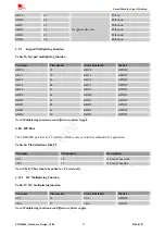
Page 39: ...3 KBR3 41 KBR3 GPIO24 KBR4 40 KBR4 GPIO25 Note Multiplexing function needs different software supply 4 10 I2C Bus The SIM2000S provides an I2 C interface which is only used in the embedded AT application Table 26 Pin definition of the I2 C Pin name Pin number Description SCL 38 I2C serial bus clock SDA 37 I2C serial bus data Note The I2C bus should be pulled to 1 8V externally 4 10 1 I2C Multiplex...

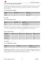
Page 40: ...rovides two auxiliary ADC which can be used to measure the voltage User can use AT command AT CADC to read the voltage value For details of this AT command please refer to document 1 Table 30 ADC specification Parameter Min Typ Max Unit Voltage range 0 2 5 V ADC Resolution 12 bits Sampling rate 2 4 MHz ADC precision 20 30 mV 4 13 PWM Table 31 Pin definition of the PWM Pin name Pin number Descripti...

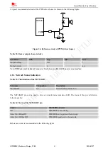
Page 41: ... low power level when module is in the power on procedure 4 14 Network Status Indication Table 33 Pin definition of the NETLIGHT Pin name Pin number Description NETLIGHT 52 Network Status Indication The NETLIGHT pin can be used to drive a network status indication LED The status of this pin is listed in following table Table 34 Status of the NETLIGHT pin Status SIM2000S behavior Off SIM2000S is no...

Page 42: ...he pin output is high when module is powered on and output is low when module is powered off Table 36 Pin definition of the STATUS Pin name Pin number Description STATUS 66 operating Status Indication 4 16 1 STATUS Multiplexing Function Table 37 STATUS multiplexing function Pin name Pin number Mode 0 default Mode 1 STATUS 66 STATUS GPIO32 Note Multiplexing function needs different software supply ...

Page 43: ...cuit 59 MODULE SIM2000S_Hardware_Design_V1 00 43 2014 02 27 R2 C1 60 RF_ANT GND C2 61 GND R1 Antenna feed pad Matching circuit RF test connector J1 J2 Figure 38 Antenna matching circuit In this figure the components R1 C1 C2 and R2 are used for antenna matching the value of components can only be got after the antenna tuning usually they are provided by antenna vendor By default the R1 R2 are 0 oh...

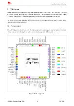
Page 44: ...t at beginning will save development schedule and cost as well This section will give some guidelines on PCB layout in order to eliminate interfere or noise by greatest degree and save product development period 5 1 Pin Assignment Before PCB layout we should learn well about pin assignment in order to get reasonable layout with so many external components Following figure is the overview of pin as...

Page 45: ... source to VBAT pin should go though Zener diode then huge capacitor Pin 53 Pin 54 Pin 63 Pin64 and Pin65 are GND signals and shortest layout to GND of power source should be designed 5 2 3 RUIM Card Interface RUIM card holder will take large space on board and there is no anti EMI component inside Thus RUIM card interface maybe interfered please pay more attention on this interface during layout ...

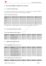
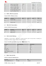
Page 46: ... as keypad GPIO I2C UART LCD and PCM 6 2 Recommended Operating Conditions Table 39 Recommended operating conditions Symbol Parameter Min Typ Max Unit VBAT Power supply voltage 3 4 3 8 4 4 V TOPER Operating temperature 40 25 85 TSTG Storage temperature 45 90 6 3 Digital Interface Characteristics Table 40 Digital interface characteristics 1 8V Symbol Parameter Min Typ Max Unit VIH High level input v...

Page 47: ...6 5 VDD_EXT Characteristics Table 43 VDD_EXT characteristics Symbol Parameter Min Typ Max Unit VO Output voltage 2 70 2 85 2 90 V IO Output current 5 mA 6 6 Electro Static Discharge SIM2000S is an ESD sensitive component so attention should be paid to the procedure of handling and packaging The ESD test results are shown in the following table Table 44 The ESD characteristics Temperature 25 Humidi...

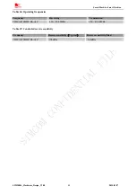
Page 48: ...0 48 2014 02 27 Table 46 Operating frequencies Frequency Receiving Transmission CDMA 450MHZ Block C 460 464 8MHz 450 454 8MHz Table 47 Conducted receive sensitivity Frequency Receive sensitivity Typical Receive sensitivity Max CDMA 450MHZ Block C 108dBm 106dBm ...

Page 49: ...Decision 7 Manufacturing 7 1 Top and Bottom View of SIM2000S Figure 40 Top and bottom view of SIM2000S 7 2 Typical Solder Reflow Profile Figure 41 Typical solder reflow profile SIM2000S_Hardware_Design_V1 00 49 2014 02 27 ...

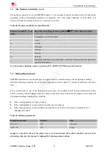
Page 50: ...ed 7 4 Baking Requirements SIM2000S modules are vacuum packaged and guaranteed for 6 months storage without opening or leakage under the following conditions the environment temperature is lower than 40 and the air humidity is less than 90 If the condition meets one of the following shown below the modules should be baked sufficiently before re flow soldering and the baking condition is shown in t...

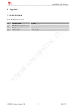
Page 51: ...ne Smart Decision SIM2000S_Hardware_Design_V1 00 51 2014 02 27 8 Appendix I Related Documents Table 50 Related documents SN Document name Remark 1 SIM2000S Series AT Command Manual 2 AN Serial Port AN Serial Port ...

Page 52: ...ile Originated MS Mobile Station CDMA engine also referred to as TE MT Mobile Terminated PAP Password Authentication Protocol PBCCH Packet Broadcast Control Channel PCB Printed Circuit Board PDU Protocol Data Unit PPP Point to point protocol RF Radio Frequency RMS Root Mean Square value RX Receive Direction SMS Short Message Service TE Terminal Equipment also referred to as DTE TX Transmit Directi...

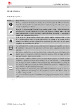
Page 53: ...nal or mobile receives and transmits radio frequency energy while switched on RF interference can occur if it is used close to TV sets radios computers or other electric equipment Road safety comes first Do not use a hand held cellular terminal or mobile when driving a vehicle unless it is securely mounted in a holder for hands free operation Before making a call with a hand held terminal or mobil...

Page 54: ..._Hardware_Design_V1 00 54 2014 02 27 Contact us Shanghai SIMCom Wireless Solutions Co Ltd Address Building A SIM Technology Building No 633 Jinzhong Road Shanghai P R China 200335 Tel 86 21 3252 3300 Fax 86 21 3252 3020 URL www sim com wm ...

Reviews: