


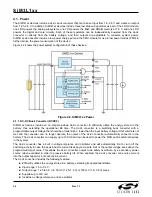


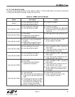


S i M 3 L 1 x x
Rev 1.1
31
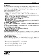
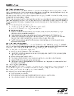
3.3. Absolute Maximum Ratings
Table
3.18.
Absolute Maximum Ratings
Parameter
Symbol
Test Condition
Min
Max
Unit
Ambient Temperature Under Bias
T
BIAS
–55
125
°C
Storage Temperature
T
STG
–65
150
°C
Voltage on VBAT/VBATDC
V
BAT
V
SS
–0.3
4.2
V
Voltage on VDC
V
DC
V
SSDC
–0.3
4.2
V
Voltage on VDRV
V
DRV
V
SS
–0.3
4.2
V
Voltage on VIO
V
IO
V
SS
–0.3
4.2
V
Voltage on VIORF
V
IORF
V
SS
–0.3
4.2
V
Voltage on VLCD
V
LCD
V
SS
–0.3
4.2
V
Voltage on I/O (PB0, PB1, PB3, PB4) or
RESET
V
IN
V
IO
> 3.3
V
V
SS
–0.3
5.8
V
V
IO
< 3.3
V
V
SS
–0.3
V
IO
+2.5
V
Voltage on PB2 I/O Pins
V
IN
V
IORF
> 3.3
V
V
SS
–0.3
5.8
V
V
IORF
< 3.3
V
V
SS
–0.3
V
IORF
+2.5
V
Total Current Sunk into Supply Pins
I
SUPP
VBAT/VBATDC, VIO,
VIORF, VDRV, VDC,
VLCD
—
400
mA
Total Current Sourced out of
Ground Pins
I
VSS
V
SS,
V
SSDC
400
—
mA
Current Sourced or Sunk by any I/O Pin
I
PIO
All I/O and RESET
–100
100
mA
Power Dissipation at T
A
=
85
°C
P
D
TQFP-80 Packages
—
500
mW
QFN-64 Packages
—
800
mW
TQFP-64 Packages
—
650
mW
QFN-40 Packages
—
650
mW
Notes:
1.
Exceeding the minimum V
IO
voltage may cause current to flow through adjacent device pins.
2.
VSS and VSSDC provide separate return current paths for device supplies, but are not isolated. They must always be
connected to the same potential on board.
Stresses above those listed under Table
3.18 may cause permanent damage to the device. This is a stress rating
only and functional operation of the devices at those or any other conditions above those indicated in the operation
listings of this specification is not implied. Exposure to maximum rating conditions for extended periods may affect
device reliability.
Summary of Contents for SiM3L1xx
Page 2: ...2 Rev 1 1 ...
Page 62: ...SiM3L1xx 62 Rev 1 1 6 2 SiM3L1x6 Pin Definitions Figure 6 2 SiM3L1x6 GQ Pinout ...
Page 63: ...SiM3L1xx Rev 1 1 63 Figure 6 3 SiM3L1x6 GM Pinout ...
Page 69: ...SiM3L1xx Rev 1 1 69 6 3 SiM3L1x4 Pin Definitions Figure 6 4 SiM3L1x4 GM Pinout ...
Page 74: ...SiM3L1xx 74 Rev 1 1 6 4 TQFP 80 Package Specifications Figure 6 5 TQFP 80 Package Drawing ...
Page 81: ...SiM3L1xx Rev 1 1 81 6 6 TQFP 64 Package Specifications Figure 6 9 TQFP 64 Package Drawing ...
Page 89: ...SiM3L1xx Rev 1 1 89 Figure 7 3 SiM3L1x4 GM Revision Information ...