Silicon Laboratories RF-to-USB-RD2 User Manual Download Page 10

R F - t o - U S B - R D 2

10

Rev. 0.2

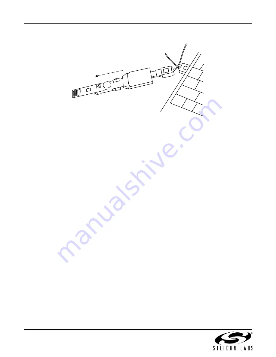
8. Remove the Node board from the ToolStick Debug Adapter as shown in Figure 17.

Figure 17. Remove Node Board from Toolstick Adapter

9. Repeat for the second Node board.

Summary of Contents for RF-to-USB-RD2

Page 1: ...nt example uses two node boards to communicate to each other A simple code example is provided as a jump start for custom projects Peripheral or low power functionality can be added to this example by referencing an available library of code examples This system is intended to be a simple starting point For more advanced radio or peripheral evaluation a full Si1000DK development kit is recommended...

Page 2: ...o exe 4 Click Connect to establish communication with the dongle as shown in Figure 2 Figure 2 Click Connect Note If an old firmware warning is received click yes to update as shown in Figure 3 Figure 3 Old Firmware Warning 5 Insert the battery into one of the node boards as shown in Figure 4 Figure 4 RF USB Node Battery In AAA ...

Page 3: ...ssociate the board with the dongle and PC application and press the button as shown in Figure 6 a Press the button Figure 6 RF USB Node Button Press b Note that the first board is assigned as Node 1 Figure 7 Figure 7 First Node Assigned as Node 1 BATT OFF TS 3 3V S2 D1 G D2 R S1 BATT OFF TS 3 3V S2 D1 G D2 R S1 ...

Page 4: ...tentiometer 4 Touch the Si1014 package to warm the internal temperature sensor as shown in Figure 9 Figure 9 RF USB Node Temperature Changes Note The node board transmits periodically for a fixed time then goes to sleep Press the button again to restart BATT OFF TS 3 3V S2 D1 G D2 R S1 BATT OFF TS 3 3V S2 D1 G D2 R S1 ...

Page 5: ...llow 4 1 PC Application Features Figure 10 RF to USB Network Demo 1 USB Dongle ID Each dongle has a unique identifier In the case of two or more dongles connected to the PC this window lets you select which one you would like to connect to 2 Connect Disconnect This button establishes or removes a connection between the PC application and a specific dongle 3 Identify In the case of two or more dong...

Page 6: ...the node boards then reassociating each by pressing its button 5 Temperature Window This displays the node s temperature as measured by the Si1014 s on chip temp sensor The node will transmit temperature data periodically then enter a low power sleep mode after several seconds Press the node s button to wake and send again 6 Potentiometer Window This displays a normalized ADC reading from the node...

Page 7: ...d and installed This software example is a simple two way link Pressing the button on one node increments a counter and sends that value to the other node which displays it on two LEDs The software example is based on the PreProcessor PHY ppPhy a free software library from Silicon Labs which manages much of the radio configuration and interface More information on the ppPhy is available in AN474 S...

Page 8: ... 11 Power Switch to TS 3 3 V 3 Plug the node board in to the ToolStick Programming Adapter and connect the adapter to your PC s USB port as shown in Figure 12 Figure 12 Connect Adapter to PC USB Port 4 Connect the IDE to the programming adapter and Node Board as shown in Figure 13 Figure 13 Connect IDE to Programming Adapter and Node Board 5 Build and download the project as shown in Figure 14 Fig...

Page 9: ...RF to USB RD2 Rev 0 2 9 6 Verify successful build and download as shown in Figure 15 Figure 15 Verify Successful Build and Download 7 Disconnect the IDE as shown in Figure 16 Figure 16 Disconnect IDE ...

Page 10: ...RF to USB RD2 10 Rev 0 2 8 Remove the Node board from the ToolStick Debug Adapter as shown in Figure 17 Figure 17 Remove Node Board from Toolstick Adapter 9 Repeat for the second Node board ...

Page 11: ...tery in Node Board 2 Slide the power switch to BATT Figure 19 Slide Power Switch to BATT 3 Press the button and observe the LEDs change on the other node board with each press Figure 20 LEDs on Other Node Board Change with Press AAA BATT OFF TS 3 3V S2 D1 G D2 R S1 BATT OFF TS 3 3V S2 D1 G D2 R S1 BATT OFF TS 3 3V S2 D1 G D2 R S1 ...

Page 12: ...t PortInit SPI1_Init Then the radio is initialized by the ppPhy status ppPhyInit status ppPhyInitRadio These functions are included in ppPhy c Refer to AN474 Si1000 Code Examples and AN440 Si4430 31 32 Register Descriptions for additional detail Next enable the interrupts and turn on the radio to receive any incoming packets EA 1 status ppPhyRxOn Once initialized the firmware loops checking for ei...

Page 13: ..._GRN EXTINGUISH LED_RED EXTINGUISH break if RX while 1 The firmware sits in this loop indefinitely and waits for a transmit request keypress or an incoming packet This is a very simple code example You may extend this example to suit your application by Adding power management See code examples in C SiLabs MCU Examples Si101x SleepMode to place the MCU core in low power waking up on keypress or a ...

Page 14: ...d in PADS Gerber and PDF formats are available from the Silicon Laboratories website The RF to USB dongle is intended more as a fixed demonstration tool Silicon Laboratories will gladly provide PCB source files in Eagle and Gerbers but the dongle is not intended for development work since it does not have a convenient debugging interface Note also that there is a solar powered energy harvesting ve...

Page 15: ...inals The switch should be left in this position for any low power application since this represents the case of a battery connected directly to the MCU dc dc converter input 8 ToolStick Adapter Interface Interface includes 3 3 V regulated power derived from USB 5 V supply C2 programming debugging interface UART interface via ToolStick Terminal 9 Test Prototype Points DC DC converter input voltage...

Page 16: ...RF to USB RD2 16 Rev 0 2 6 PCB Schematics and Layouts Figure 22 Node Schematic ...

Page 17: ...RF to USB RD2 Rev 0 2 17 Figure 23 Dongle Schematic ...

Page 18: ...RF to USB RD2 18 Rev 0 2 Figure 24 Node PCB Layout L1 Top Figure 25 Node PCB Layout L2 Gnd Figure 26 Node PCB Layout L3 Gnd ...

Page 19: ...RF to USB RD2 Rev 0 2 19 Figure 27 Node PCB Layout L4 Bottom ...

Page 20: ...RF to USB RD2 20 Rev 0 2 Figure 28 Dongle PCB Layout L1 Top Figure 29 Dongle PCB Layout L2 ...

Page 21: ...RF to USB RD2 Rev 0 2 21 Figure 30 Dongle PCB Layout L3 Figure 31 Dongle PCB Layout L4 Bottom ...

Page 22: ...RF to USB RD2 22 Rev 0 2 Figure 32 Dongle PCB Layout Top Assembly Figure 33 Dongle PCB Layout L4 Bottom Test Points ...

Page 23: ...ata rate is 128 kbps using GFSK modulation Both demo applications use EZMAC PRO channel 19 The output power is 13 dB for both the USB Dongle and Sensor Node The PCB antennas on both Sensor Node and USB Dongle are designed for lowest possible cost not maximum range For firmware source code or additional information contact MCU support http www silabs com support ...

Page 24: ...RF to USB RD2 24 Rev 0 2 DOCUMENT CHANGE LIST Revision 0 1 to Revision 0 2 Content completely revised ...

Page 25: ...RF to USB RD2 Rev 0 2 25 NOTES ...

Page 26: ...ein Additionally Silicon Laboratories assumes no responsibility for the functioning of undescribed features or parameters Silicon Laboratories reserves the right to make changes without further notice Silicon Laboratories makes no warranty rep resentation or guarantee regarding the suitability of its products for any particular purpose nor does Silicon Laboratories assume any liability arising out...

Reviews: