


C 8 0 5 1 T 6 2 0 / 2 - D K
Rev. 0.4
15
7.4. USB Debug Adapter (DEBUG/P5)
A Universal Serial Bus (USB) connector (P5) provides the onboard debug and programming interface. The debug/
programming MCU and associated circuitry are powered through the USB connector, which can also supply the
rest of the motherboard by routing the USB Debug Adapter's power through J6. The USB Debug Adapter also
provides a data communications interface that can be used when the debug adapter is not debugging or
programming a C8051T62x/32x device.
7.5. UART to USB Communications Interfaces (COMM/P4)
The C8051T62x Motherboard provides UART to USB communications interfaces through both the CP2103 USB-
to-UART bridge device and the communications interface of the USB Debug Adapter.
The CP2103 bridge device connects to a PC through the USB connector labeled “COMM” (P4). This USB
connector supplies power to the CP2103 and can supply power to the rest of the motherboard by configuring J6
and J7 as shown in Figure 12. To use the CP2103 as a communications interface, the CP2103 Virtual COM Port
drivers must be installed on a PC.
The USB Debug Adapter's communications interface connects to a PC through P5. Access to the USB Debug
Adapter's communications interface is provided by the Windows program called “ToolStick Terminal”, which is
available for download for free from the Silicon Laboratories website. See the ToolStick Terminal help file for
information on how to use ToolStick Terminal.
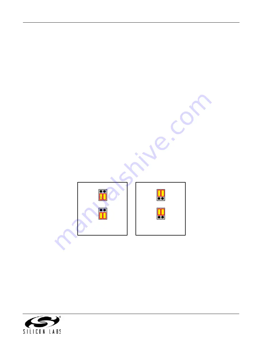
7.6. Communications Interface Selector Headers (J8 and J11)
The C8051T62x Motherboard routes the C8051T62x/32x's P0.4 (UART TX) and P0.5 (UART RX) to J11 where
those signals can be connected to either the CP2103 USB-To-UART bridge or the USB Debug Adapter. The
motherboard also allows the C8051T62x/32x's P1.1 and P1.2 to be used as the UART control signals, CTS and
RTS. These two signals are routed to J8, where they can be connected to either the CP2103 or the USB Debug
Adapter.
The jumper options for using either the CP2103 or the Debug Adapter circuit for UART communications can be
found in Figure 13.
Figure 13. Shorting Block Configuration for UART Communication Options
7.7. PORT I/O Connectors (J2, J3, J4, and J5)
Each of the C8051T62x/32x's I/O pins, as well as +3VD and GND, are routed to headers J2 through J5. J2
connects to the microcontroller's Port 0 pins; J3 connects to Port 1; J4 connects to Port 2, and J5 connects to
Port 3.
CTS_DEBUG
P1.1
P1.2
RTS_COMM
CTS_COMM
RTS_DEBUG
J8
CTS_DEBUG
P0.4
P0.5
RX_COMM
CTS_COMM
RX_DEBUG
J11
CP2103 Bridge
(USB Connection at P4)
RTS_DEBUG
P1.1
P1.2
RTS_COMM
CTS_COMM
RTS_DEBUG
J8
TX_DEBUG
P0.4
P0.5
RX_COMM
TX_COMM
RX_DEBUG
J11
Debug Adapter Comms
(USB Connection at P5)
Summary of Contents for C8051T620-DK
Page 18: ...C8051T620 2 DK 18 Rev 0 4 8 Schematics Figure 14 C8051T62x Motherboard Schematic 1 of 2 ...
Page 19: ...C8051T620 2 DK Rev 0 4 19 Figure 15 C8051T62x Motherboard Schematic 2 of 2 ...
Page 20: ...C8051T620 2 DK 20 Rev 0 4 Figure 16 C8051T62x Emulation Daughter Board Schematic ...
Page 21: ...C8051T620 2 DK Rev 0 4 21 Figure 17 C8051T620 QFN 32 Daughter Board Schematic ...
Page 22: ...C8051T620 2 DK 22 Rev 0 4 Figure 18 C8051T622 QFN 24 Daughter Board Schematic ...
Page 23: ...C8051T620 2 DK Rev 0 4 23 Figure 19 C8051T320 QFP 32 Daughter Board Schematic ...
Page 24: ...C8051T620 2 DK 24 Rev 0 4 Figure 20 C8051T321 QFN 28 Daughter Board Schematic ...
Page 25: ...C8051T620 2 DK Rev 0 4 25 Figure 21 C8051T326 QFN 28 Daughter Board Schematic ...
Page 26: ...C8051T620 2 DK 26 Rev 0 4 Figure 22 C8051T327 QFN 28 Daughter Board Schematic ...


