


C 8 0 5 1 F 0 0 x / 0 1 x - D K
Rev. 0.6
5
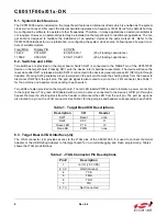
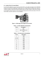
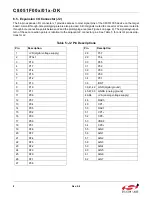
6. Target Board
The C8051F00x/01x Development Kit includes a target board with a C8051F005 device pre-installed for evaluation
and preliminary software development. Numerous input/output (I/O) connections are provided to facilitate prototyp-
ing using the target board. Refer to Figure 2 for the locations of the various I/O connectors.
P1
Power connector (accepts input from 7 to 15 VDC unregulated power adapter)
J1
Connects SW2 to port pin P1.7
J2
64-pin I/O connector providing access to all I/O signals
J3
Connects LED D3 to port pin P1.6
J4
JTAG connector for Debug Adapter interface
J6
Analog I/O configuration connector
X1
Analog I/O terminal block
Figure 2. C8051F005 Target Board
J3
J1
P1
Pr
o
to
A
re
a
Pr
o
to
Ar
e
a
J
2
Pin 1
Prototyping Area I/O Connection Points
J
6
Pin 2
P1.7
RESET
PW
R
P1.6
Pin 1
JT
A
G
C8051F005
Pin 1
Pin 2
X1


