background image


41110461XXX 

Rev 0.1 

January 16, 2017 

17 

Hardware Integration Guide 

Introduction 

1.5. 

Electrical Specifications 

This section provides details of the key electrical specifications of the AirPrime AR758x Series. 

1.5.1. 

Absolute Maximum Ratings 

This section defines the Absolute Maximum Ratings of the AirPrime AR758x Series. 

Warning:  

If operating outside of the defined specifications, even momentarily, damage may occur to the 
device. 

Table 16. 

AirPrime AR758x Series Absolute Maximum Ratings 

Parameter 

Min 

Max 

Units 

VBATT 

Power Supply Input 

4.5 

VIN 

Voltage on any digital input or output pin 

Vxx + 20%* 

IIN 

Latch-up current 

-100 

100 

mA 

ESD Ratings 

ESD

1


Primary, Secondary and GNSS antenna pads 

– 

Contact 

± 8 

kV 

All other signal pads 

– Contact 

± 1.5 

kV 

1 The ESD Simulator configured with 150pF, 330

Ω. 

Caution: 

 Vxx is the supply voltage associated with the input or output pin to which the test voltage is applied. 

1.5.2. 

Digital IO Characteristics 

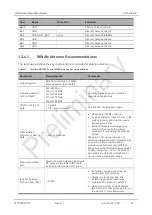
The Digital IO characteristics are defined in the table below. These apply to GPIOs, UART, LED, SPI, 
I2C, PCM/I2S, GNSS_LNA, WAKE_N, 2G_SYNC, AT_PORT_SW, SERVICE and RESET. 

Table 17. 

Digital IO Characteristics for HSIC VDD=1.2V Nominal 

Parameter 

Comments 

Min 

Typ 

Max  

Units 

V

IH


High level input voltage  

CMOS/Schmitt 

0.78 

– 

1.44 

V

IL


Low level input voltage 

CMOS/Schmitt  

-0.3 

– 

0.42 

I

IH


Input high leakage current 

No pull-down 

– 

– 

µA  

I

IL


Input low leakage current 

No pull-up 

-2 

– 

– 

µA 

V

OH


High-level output voltage 

CMOS, at rated drive 
strength 

0.9 

– 

1.25 

V

OL


Low level output current 

CMOS, at rated drive 
strength 

– 

0.3 

I

Z


Tri-state leakage current 

No pull, no keeper 

-2 

– 

µA 

C

IN


Input capacitance 


– 

– 

pF 


Summary of Contents for AirPrime AR7582-1

Page 1: ...4111xxxx 0 1 Nov 17 2017 AirPrime AR7582 1 Hardware Integration Guide...

Page 2: ...erfere with various onboard systems Note Some airlines may permit the use of cellular phones while the aircraft is on the ground and the door is open Sierra Wireless modems may be used at this time Th...

Page 3: ...logos are registered trademarks of Sierra Wireless Inc or one of its subsidiaries Watcher is a registered trademark of Netgear Inc used under license Windows and Windows Vista are registered trademar...

Page 4: ...41110461XXX Rev 0 1 January 16 2017 4 Hardware Integration Guide Document History Version Date Updates 0 1 November 16 2017 Creation...

Page 5: ...2 GNSS Antenna Interface 16 1 4 2 1 GNSS Antenna Recommendations 16 1 5 Electrical Specifications 17 1 5 1 Absolute Maximum Ratings 17 1 5 2 Digital IO Characteristics 17 2 AUDIO SPECIFICATION 20 2 1...

Page 6: ...41110461XXX Rev 0 1 January 16 2017 6 Hardware Integration Guide 7 ABBREVIATIONS 30...

Page 7: ...Figure 1 AppCAD Screenshot for Microstrip Design Power Mode Diagram 21 Figure 2 RF Routing Examples 22 Figure 3 Coplanar Clearance Example 22 Figure 4 Antenna Microstrip Routing Example 23 Figure 5 Ai...

Page 8: ...LTE Bands 12 Table 11 Conducted RX Sensitivity 3GPP BW 10MHz LTE Bands1 4 13 Table 12 Conducted RX Sensitivity SISO BW 10MHz LTE Bands1 13 Table 13 WWAN Antenna Interface Pads 13 Table 14 AirPrime AR...

Page 9: ...GE 850 1900 North America Canada US Mexico 1 Other regions or operators which use the same frequency bands may also be supported subject to review and confirmation by Sierra Wireless Optional band 1 2...

Page 10: ...B 30 2 5dB GSM 850 27 3dB 27 4dB 27 2 5dB 27 3 5dB 8PSK mode connectorized Class E2 0 5 W 27 dBm EGSM 900 27 3dB 27 4dB 27 2 5dB 27 3 5dB GSM 1800 26 3dB 26 4dB 26 2 5dB 26 3 5dB 8PSK mode connectoriz...

Page 11: ...3 5 2 2 2 7dB B6 24 1 7 3 7dB 23 5 2 2 2 7dB 23 5 2 2 2 7dB 1 Connectorized Class 3 2 Per 3GPP TS 34 121 1 Specification 3 Test at Class A extreme condition 1 3 2 2 WCDMA RX Sensitivity The WCDMA Rece...

Page 12: ...1 The test configurations for all of the entries in the table above are per 3GPP specification Connectorized Class 3 Note 2 Per 3GPP TS 36 521 1 6 2 2 UE Maximum Output Power No MPR and for B13 Per V...

Page 13: ...tivity values scale with bandwidth x_MHz_Sensitivity 10 MHz_Sensitivity 10 log 10 MHz x_MHz 10 MHz BW and 50 RB DownLink and Up Link as 3GPP TS 36 521 1 Table 7 3 5 2 All values are preliminary pendin...

Page 14: ...nd edges Total radiated efficiency of Ant1 or Ant2 50 on all bands Measured at the RF connector Includes mismatch losses losses in the matching circuit and antenna losses excluding cable loss Sierra W...

Page 15: ...ts as the complex match between the module and antenna can cause unwanted levels of emissions Tuning may include antenna pattern changes phase delay adjustment passive component matching Examples of t...

Page 16: ...Pre SAW and LNA for conducted test setup at Room temperature it is used to simulate the active antenna as customer s application 5 1Hz Navigation used for all tracking navigation tests 6 GNSS constel...

Page 17: ...other signal pads Contact 1 5 kV 1 The ESD Simulator configured with 150pF 330 Caution Vxx is the supply voltage associated with the input or output pin to which the test voltage is applied 1 5 2 Digi...

Page 18: ...output current VOH 1 35 V 6 mA IOL Low Level output current VOL 0 45 V 6 mA IOH PM High level output current GPIO_PMxx only 0 60 mA IIHPD Input high leakage current Logic High with pull down 5 33 A II...

Page 19: ...S Schmitt 0 7 UICC_VCC UICC_VCC 0 3 V VIL Low level input voltage CMOS Schmitt 0 3 0 2 UICC_VCC V IIH Input high leakage current No pull down 10 A IIL Input low leakage current No pull up 10 A VOH Hig...

Page 20: ...I2 S I2S_WS I2 S Word Select DC2 PCM PCM_DOUT Output PCM Data Out Leave Open I2 S I2S_DOUT I2 S Data Out DD2 PCM PCM_DIN Input PCM Data In Leave Open I2 S I2S_DIN I2 S Data In DD3 PCM2 PCM_CLK Output...

Page 21: ...f the material used trace width W trace thickness T and height H between the trace and the reference ground plane In order to respect this constraint Sierra Wireless recommends that a MicroStrip struc...

Page 22: ...corners A smooth radius is recommended E g Use of 45 angles instead of 90 The ground reference plane should be a solid continuous plane under the trace The coplanar clearance G below from the trace to...

Page 23: ...adjacent signals SuperSpeed USB adds two differential pairs SSRX SSRX and SSTX SSTX These pairs should be routed with the following considerations constraints 90 Ohm differential 15 trace impedance D...

Page 24: ...e voltage translation This allows a host processor operating at a different voltage to communicate with the AirPrime AR758x Series using the appropriate voltage levels The figure below is a reference...

Page 25: ...CDMA air interface protocols GNSS engine IMS protocol stack AT Command Processor New AT commands will be added by Sierra Wireless See document 8 for the complete list of AT Commands for AR758x AR8582...

Page 26: ...with this equipment In an aircraft the AirPrime AR7582 1 device MUST BE POWERED OFF Otherwise the AirPrime AR7582 1 device can transmit signals that could interfere with various onboard systems and ma...

Page 27: ...4 5 824 849 3 12 699 716 3 13 777 787 3 17 704 716 3 UMTS 2 1850 1910 5 4 1710 1755 4 5 824 849 3 GPRS 2 1850 1910 5 5 824 849 3 EDGE 2 1850 1910 5 5 824 849 3 Collocated transmitters WLAN 2400 2500...

Page 28: ...5 4 1 Radiation Exposure Statement This equipment complies with Canada radiation exposure limits set forth for an uncontrolled environment This equipment should be installed and operated with minimum...

Page 29: ...enters Forum 6 Universal Serial Bus Class Definitions for Communication Devices V1 1 USB Implementers Forum 7 AirPrime AR7 Series Customer Process Guidelines Sierra Wireless 8 AirPrime AR75xx AT Comma...

Page 30: ...mmunications HSPA High Speed Packet Access I2S Inter IC Sound LTE Long Term Evolution PCIe Peripheral Component Interconnect Express PCM Pulse Coded Modulation PMIC Power Management Integrated Circuit...

Reviews: