background image

2-25

SIMATIC PC RI25/45, Technical Description
C79000-G7076-C808-01

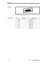
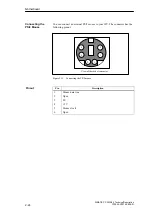
The MPI/DP socket connector has the following pinout:

1

5

6

9

Figure 2-12

MPI/DP socket connector

Pin No.

Abbreviation

Description

Input/

Output

1

NC

Pin 1 is unassigned

2

NC

Pin 2 is unassigned

3

LTG_B

Data line B

Input/
Output

4

RTSAS

RTSAS control signal for receive
data current. Signal ’1’ is active
when the directly linked
programmable controller transmits
data.

Input

5

M5EXT

M5EXT Ground (GND) of 5 V
supply. The current load of an
external consumer connected
between P5EXT and M5EXT must
not exceed a maximum of 90 mA.

Output

6

P5 EXT

P5EXT supply (+5 V) of 5V
supply. The current load of an
external consumer connected
between P5EXT and M5EXT must
not exceed a maximum of 90 mA.

7

NC

Pin 7 is unassigned

8

LTG_A

Data line A

Input/
Output

9

RTS_PG

RTS output signal. The signal is ’1’
when your IPC starts transmitting.

Output

Shield

On connector shell

MPI/DP Port

Pinout

Motherboard

Summary of Contents for SIMATIC PC RI25/45

Page 1: ...nit 1 Motherboard 2 Bus Board 3 Monitoring Module 4 Hard Disk Drive 5 Floppy Disk Drive 6 CD ROM Drive 7 Back Up Battery 8 220 V Power Supply 9 Index C79000 G7076 C808 01 SIMATIC PC RI25 45 SIMATIC Technical Description ...

Page 2: ...description and only in connection with devices or components from other manufacturers which have been approved or recommended by Siemens This product can only function correctly and safely if it is transported stored set up and installed correctly and operated and maintained as recommended SIMATICR SIMATIC NETR and SINECR are registered trademarks of SIEMENS AG Third parties using for their own p...

Page 3: ...he Display Board 1 13 1 3 9 Removing and Installing Module Retainers only RI45 RI45PCS 1 14 1 3 10 Removing and Installing Expansion Modules 1 15 1 3 11 Removing and Installing the Bus Board 1 15 1 3 12 Removing and Installing the CPU Board 1 16 1 3 13 Connecting the Multipoint Interface MPI DP 1 17 1 4 Error Diagnostics 1 18 2 Motherboard 2 1 2 1 Components 2 2 2 2 Processor 2 3 2 3 Cache Modules...

Page 4: ...r SafeCard 3 8 4 Monitoring Module 4 1 4 1 Overview 4 2 4 2 Status and Diagnostic Displays 4 5 4 3 Temperature Monitoring Display and Fan Control 4 6 4 4 Watchdog WD 4 7 4 5 Relay Output 4 9 4 6 Battery Backed RAM optional 4 10 4 7 Software Interfaces 4 11 4 8 Hardware Ports 4 14 5 Hard Disk Drive 5 1 5 1 Technical Specifications 5 2 6 Floppy Disk Drive 6 1 6 1 Technical Specifications 6 2 7 CD RO...

Page 5: ... and Installing Fans 1 9 1 3 5 Removing and Installing the 3 5 Floppy Disk Drive 1 10 1 3 6 Removing and Installing the Drive Block Front 1 11 1 3 7 Removing and Installing Hard Disk Drives Back 1 12 1 3 8 Removing and Installing the Display Board 1 13 1 3 9 Removing and Installing Module Retainers only RI45 RI45PCS 1 14 1 3 10 Removing and Installing Expansion Modules 1 15 1 3 11 Removing and Ins...

Page 6: ...imensions indicated If the given height is exceeded this may cause contacting problems functional disorders or difficulties with installation The figures below illustrate two cards with full AT PCI overall length Individual slots may require different card dimensions 340 7 106 7 A31 A1 All dimensions in mm Figure 1 1 XT module 340 7 121 92 A31 A1 All dimensions in mm C18 C1 Figure 1 2 AT module In...

Page 7: ... 68 8 19 All dimensions in mm Figure 1 4 Large PCI module 5 V Large PCI modules have to be equipped with a so called extender usually included with large PCI modules which serves to guide them along the rails of the ventilator case The extender guides large PCI modules along the rails of ISA modules Information on Large PCI Modules System Unit ...

Page 8: ...Motherboard 5 1 A 0 01 A 0 1 A 0 02 A SafeCard monitoring module 0 35 A 0 03A Front fan 0 5 A 3 5 floppy disk drive Hard disk see Section 5 1 Due to thermal stress the maximum capacity of the power supply is restricted to Power supply Restriction Standard power supply 220 V maximum load 160 W Basic System Restrictions on Power Supply System Unit ...

Page 9: ...rranty on the device is not affected Authorized Siemens maintenance and repair centers offer you a specialist maintenance service The User s Guide contains the addresses Caution The electronic components of the printed boards are extremely sensitive to electrostatic discharge When handling the boards you must follow the guidelines for electrostatically sensitive components ESD guidelines at the en...

Page 10: ...Discharge any electrostatic charge from tools that you are using Wear a grounding wrist strap if you are handling components Leave components and modules in their packing until you are ready to install them Disconnect the PC from its power supply before plugging in or removing any modules or components Touch components and modules only on their edges Above all do not touch the connecting pins and ...

Page 11: ...he protective grid protects you from injuring yourself on the sharp edges of the fan and prevents the filter pad from being sucked into the fan Caution When the fans are operating particles can be drawn into the system unit The protective grid may only be removed with the PC switched off 1 3 2 Removing the Protective Sliding Cover Please note the following if the protective cover has to be removed...

Page 12: ...ve and hard disk drive power supply fan cage with two fans Two fans 3 5 floppy disk drive Rear support for hard disk drives only with RI45 Bus board Fan cage Safe Card Front drive block Represented without crossbeam with retainers Motherboard Power supply Figure 1 6 SIMATIC PC RI First remove the screws at the top Hold the cover at its front left and right edges lift it up and off by sliding it ba...

Page 13: ...he two clamps of the fan cage see Figure 1 7 then push the top of the two side sections outward and lift the fan cage up First the connecting cables have to be carefully removed from the bottom of the cut out then remove the two fans If expansion modules are installed you can take out the fans from the fan cage even without previously removing the expansion modules first unplug the connecting cabl...

Page 14: ...place the floppy disk drive Disconnect all the cables and write down their prevoius connections Release the two screws at the top of the drive support see arrows in Figure 1 8 and pull out the drive from the back Mounting screws Figure 1 8 Removing the floppy disk drive Proceed in reverse order to install a floppy disk drive Procedure System Unit ...

Page 15: ...ive block two centimeters 0 8 inches to the rear see direction of arrow in Figure 1 9 then pull the front block out of the housing To replace the drive or to install a second drive for example a CD ROM drive release the two upper and the two lower screws Then remove the 3 5 support which lodges the hard disk drive and release the four screws which connect hard disk drive and support 5 25 drives or...

Page 16: ...rt is mounted with three screws see Figure 1 10 Two of them are directly accessible at the back of the system unit The third screw can only be reached inside the unit from the top The hard disk drives must be fixed with screws at the upper and lower end of the support Then connect the installed hard disk drives CPU board and power supply by plugging in the corresponding connecting cables Mounting ...

Page 17: ...oard First disconnect the cables and write down the previous connections Then pry the display board out of the catches see Figure 1 11 Catches Figure 1 11 Removing the display board After unscrewing two hexagonal socket screws the right handle and the front plate the panel covering can be taken off System Unit ...

Page 18: ... retainers and crossbeam Proceed in reverse order to install the retainers Adjusting retainers Insert the sliding element at the top and push it down until it covers the module Then guide the module into the notch Caution Do not exert pressure on the module This means that you should not push down or force the retainers in any way Cut off the part of the sliding element that sticks out as describe...

Page 19: ...e the module without bending it To install the new module proceed in reverse order 1 3 11 Removing and Installing the Bus Board First remove all expansion modules Disconnect all connectiong cables or connectors and write down their previous connections Release 5 screws 2 at the front with the spacer between the CPU board and 3 screws at the back Lift the bus board out of the connector to the CPU b...

Page 20: ...wn their previous connections Release the 2 screws at the back of the system unit see arrows in Figure 1 13 then push forward the CPU board and its baseplate until it comes to a stop and lift it out You can now remove the bus board if necessary Mounting screws Figure 1 13 Removing the CPU board To install the board follow the instructions in reverse order The bus board and supporting plate are not...

Page 21: ...g in the connecting cables you must discharge the electrostatic charge of the cables and of your body by briefly touching a grounded object ESD guidelines You can network up to 32 devices PC programming device programmable logic controller or DP components via the MPI DP interface in one seg ment The interconnection to the PROFIBUS DP segments is established via an optically isolated RS 458 port w...

Page 22: ...nd no characters appear Keyboard buffer overflow CTRL PAUSE Not ready message when trying to write to a diskette No diskette has been inserted Diskette has not been formatted Insertdiskette Formatdiskette Write protect error when trying to write to a diskette Diskettewrite protectactivated Write protect hole open on 3 5 diskette Cancel write protection EPROM TSR interface disabled check Power Mana...

Page 23: ...odule 2 5 2 5 Memory 2 8 2 6 Changing the Backup Battery 2 11 2 7 Block Diagram of the Motherboard 2 12 2 8 Hardware Ports 2 13 2 9 Hardware Addresses 2 26 2 10 Interrupt and DMA Assignments 2 30 2 11 Setup 2 31 2 11 1 Main Menu 2 35 2 11 2 Advanced Menu 2 44 2 11 3 Security Menu 2 46 2 11 4 Power Menu 2 47 2 11 5 Exit Menu 2 49 2 12 Diagnostic Messages Port 80 2 51 Chapter Overview 2 ...

Page 24: ...2 4MB module 16 MB 2 8MB module 32 MB 2 16MB module 64 MB 2 32MB module 128 MB 4 32MB module Pairs can be combined EPROM 128kB flash CMOS 114 Byte CMOS RAM with battery backup Chipset Intel Triton Chipset NSC Super I O PC87306 Graphicscard SVGA LCD controller Cirrus GD7543 with Windows accelerator on PCI bus 1MB RAM with LCD up to 800x600 64 colors with CRT up to 1024x768 72Hz 256 colorspossible I...

Page 25: ...ve the exact position 4 as indicated on the slot A Caution The marks on top of the processor may be covered by the cooling unit In this case use the marks inbetween the pin rows on the outside of the processor 5 Swing the lever upwards until it clicks into position 5 6 Fix the cooling unit using the lifting lever 7 If necessary change the settings for processor frequency switch S1 S2 jumper X34 Ca...

Page 26: ...approved by your system engineering company The RI45 is supplied with a 256 KB synchronous burst cache Plug the optional cache module into connector 23 which is protected against polarity reversal and located on the motherboard see Section 2 8 Position of connectors and switches Enable the cache module in the SETUP of the system s BIOS External Cache Enabled Recommended Cache Modules Installing Ca...

Page 27: ...K 40x25 8x8 320x200 text 31 5 70 00 01 16 256K 40x25 8x14 320x350 text 31 5 70 00 01 16 256K 40x25 9x16 360x400 text 31 5 70 02 03 16 256K 80x25 8x8 640x200 text 31 5 70 02 03 16 256K 80x25 8x14 640x350 text 31 5 70 02 03 16 256K 80x25 9x16 720x400 text 31 5 70 04 05 4 256K 40x25 8x8 320x200 graphics 31 5 70 6 2 256K 80x25 8x8 640x200 graphics 31 5 70 07 mono 80x25 9x14 720x350 text 31 5 70 07 mon...

Page 28: ...C 103 256 256K 100x37 8x16 800x600 36 35 2 56 5C 103 256 256K 100x37 8x16 800x600 40 37 9 60 5C 103 256 256K 100x37 8x16 800x600 50 48 1 72 5C 103 256 256K 100x37 8x16 800x600 50 46 875 75 5D 104 16 256K 128x48 8x16 1024x768 44 9 45 5 43 5D 104 16 256K 128x48 8x16 1024x768 65 48 3 60 5D 104 16 256K 128x48 8x16 1024x768 75 56 70 5D 104 16 256K 128x48 8x16 1024x768 77 58 72 5D 104 16 256K 128x48 8x1...

Page 29: ...160x64 8x16 1280x1024 75 48 43 6D 256 256K 160x64 8x16 1280x1024 75 48 43 71 112 16M 80x30 8x16 640x480 25 31 5 60 74 64K 1024x768 44 9 35 5 43 Note Some monitors do not support all modes Your monitor automatically uses the highest vertical scan frequency signifies interlaced mode 43 5 Hz or 87 Hz interlaced signifies 32K direct or packed pixel mode Sierra The two graphics modes 11 and 12 are base...

Page 30: ...mming devices Your dealer will tell you which cards you can use Recommended memory expansion cards 8 MB 2 4MB card 16 MB 2 8MB card 32 MB 2 16MB card 64 MB 2 32MB card 128 MB 4 32MB card Pairs can be combined Only plug memory cards of the same type and make into an expansion slot Memory configuration Memory cards in expansion slot 1 2 Memory cards in expansion slot 3 4 8 MB empty 2 4 MB 16 MB empt...

Page 31: ...rews which are accessible from their top using a Torx screwdriver then lift the module and pull it out of its motherboard socket 5 Plug or unplug the SIMM cards as described below Plug in from the right to the left slot unplug in reverse order 6 Make sure that the cards are correctly plugged in as shown in Figure 2 2 7 Reassemble the unit in reverse order Correctly installed SIMM card Incorrectly ...

Page 32: ...with the centering pivot of the carrying device 2 Press the card lightly down until it locks into place 2 2 1 Figure 2 2 Installing the memory card Proceed as follows to remove a memory card 1 Press the holding clips on the left and right side carefully outwards 1 2 Tilt the memory card forward 2 and pull it diagonally out of the slot 3 2 1 1 3 Figure 2 3 Removing the memory card Installing the Me...

Page 33: ...y The battery is located underneath the bus board To change the battery please proceed as follows 1 Switch off your PC and unplug all connecting cables 2 Open the unit as described in Section 1 4 3 Remove the drive support 4 Now replace the backup battery which is attached to the motherboard by a short length of a cable 5 Reassemble the drive support and close the unit Caution You may only replace...

Page 34: ...V 5V HD8 15 24 31 40 47 56 63 MD0 7 16 23 32 39 48 55 MD8 15 24 31 40 47 56 63 PLINK8 15 PLINK0 7 D4 D5 3 3V 5V Cache 160pol Con X23 HA3 31 HD 0 63 HA3 31 control lines FrameBuffer 256x16 dRAM D12 256x16 dRAM D11 5V 5V 514171 514171 Legend 5V 3 3V VMA0 9 Taktgenerator 3 3V ICD2254 D2 14 3181MHz 25 30 33MHz Pentium Socket 7 split 3 3V 321SPGAZiff 50 60 66MHz X12 VG 469 PCMCIA CTRL VCC VPP Mem Card ...

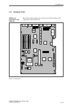
Page 35: ...ing figure illustrates the connector and switch positions of the components on the motherboard X12 X4 X3 X402 X11 X10 X800 X9 X7 1 2 3 4 5 6 S2 S1 X18 X17 Batt X24 X22 X21 X20 X19 X1 X23 X80 X90 X6 1 2 3 4 5 6 X15 CPU X34 X801 Figure 2 5 Motherboard Position of Connectors and Switches Motherboard ...

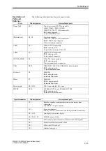
Page 36: ... socket 7 X15 Display module Port for display module cable X17 Socket Socket for TTY sender module X18 Socket Socket for TTY receiver module X19 RAM bank 1 2 low Socket for RAM X20 RAM bank 1 2 high Socket for RAM X21 RAM bank 3 4 low Socket for RAM X22 RAM bank 3 4 high Socket for RAM X23 Second level cache Socket for cache X24 Battery Connector for lithium battery X26 Fan Fan port 12V X30 Fan Fa...

Page 37: ...onnector VGA X402 3B0h 3BFh 3C0h 3CFh 3D0h 3DFh disconnectable IRQ9 edge triggered 15 pin standard connector Keyboard X6 060h 064h IRQ1 edge triggered 6 pin mini Din socket Mouse X7 060h 064h IRQ12 edge triggered 6 pin mini Din socket Power supply X80 X90 2 PS 2 connector P8 P9 6 pin MPI DP X800 0CC000h 0CC7FFn or 0DC000h 0DC7FFh IRQ5 edge triggered 9 pin sub D socket connector Specialconnector Pi...

Page 38: ... 800x600 TFT standard setting S2 1 S2 2 Function on on active TTY port standardsetting off x TTY transmission loop separate from current source passive setting x off TTYE receiving loop separate from current source passivesetting Not used on the RI25 45 S2 3 S2 4 Function off on Hardware in normal operation standard setting on x Boot EPROM disabled Boot module necessary x off Disable Boot block RO...

Page 39: ...k ratio CPU BUS CORE 1 2 or 2 5 x off x Clock ratio CPU BUS CORE 2 3 or 1 3 x x on Clock ratio ISA PCI 1 4 x x off Clock ratio ISA PCI 1 3 The effect of the switch setting S1 5 depends on jumper X34 S2 5 S2 6 Function on off 66MHz CPU bus clock standard setting off on 60MHz CPU bus clock on on 50MHz CPU bus clock off off Reserved test mode setting Jumper for Setting the CPU Type S1 Display Type an...

Page 40: ... internal on off on on 8 25MHz 33MHz 66MHz 133MHz 166MHz off on on on 7 50MHz 30MHz 60MHz 120MHz 150MHz on on on off 8 33MHz 25MHz 50MHz 100MHz on off off on 8 25MHz 33MHz 66MHz 100 233MHz 200MHz off on off on 7 50MHz 30MHz 60MHz 90MHz 180MHz on on off off 8 33MHz 25MHz 50MHz 75MHz 150MHz Preferable settings are printed in bold letters Caution Operating a processor at a higher frequency than the m...

Page 41: ...SR M1 Input 7 Functional ground GND E2 8 Data carrier detect DCD M5 Input 9 TTY Receive data RxD Input 10 TTY Receive data RxD Input 11 unassigned 12 unassigned 13 unassigned 14 unassigned 15 unassigned 16 unassigned 17 unassigned 18 TTY Transfer data TxD Output 19 Current source isolated 20 Data terminal ready DTR S1 Output 21 TTY Transfer data TxD Output 22 Incoming call RI M3 Input 23 unassigne...

Page 42: ...COM 2 serial interface Pin Abbreviations Signal Designation 1 DCD DataCarrierDetect 2 RxD ReceiveData 3 TxD TransferData 4 DTR Data TerminalReady 5 Signal Ground 6 DSR Data Set Ready 7 RTS Request to Send 8 CTS Clear to Send 9 Ri Ring Indicator COM2 Port Signal Names Motherboard ...

Page 43: ... SCSI or to an IDE port Each mode has an individual pinout 1 13 14 25 Figure 2 8 LPT1 parallel port Pin No Description Input Output 1 Strobe Output open collector 2 Data Bit 0 Output TTL level 3 Data Bit 1 Output TTL level 4 Data Bit 2 Output TTL level 5 Data Bit 3 Output TTL level 6 Data Bit 4 Output TTL level 7 Data Bit 5 Output TTL level 8 Data Bit 6 Output TTL level 9 Data Bit 7 Output TTL lev...

Page 44: ...VGA socket connector Pin Description Pin Description 1 Video signal red 9 Code no pin 2 Video signal green 10 Ground synchronization 3 Video signal blue 11 Display ID bit 0 4 Display ID Bit 2 12 Display ID bit 1 5 Ground 13 Horizontal synch 6 Ground red 14 Vertical synch 7 Ground green 15 Display ID bit 3 8 Ground blue VGA Pinout Motherboard ...

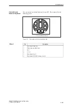
Page 45: ... your IPC The connector has the following pinout View of socket connector 1 2 3 4 5 6 Figure 2 10 Connecting cable for external keyboard Pin Description 1 Keyboard data line 2 Open mouse data line 3 0 V 4 5 V 5 Keyboard clock 6 Keyboard ON OFF mouse clock Connecting an External Keyboard Pinout Motherboard ...

Page 46: ...nnect an external PS 2 mouse to your IPC The connector has the following pinout View of the socket conenctor 1 2 3 4 5 6 Figure 2 11 Connecting the PS 2 mouse Pin Description 1 Mouse data line 2 Open 3 0 V 4 5 V 5 Mouse clock 6 Open Connecting the PS 2 Mouse Pinout Motherboard ...

Page 47: ... the directly linked programmable controller transmits data Input 5 M5EXT M5EXT Ground GND of 5 V supply The current load of an external consumer connected between P5EXT and M5EXT must not exceed a maximum of 90 mA Output 6 P5 EXT P5EXT supply 5 V of 5V supply The current load of an external consumer connected between P5EXT and M5EXT must not exceed a maximum of 90 mA 7 NC Pin 7 is unassigned 8 LT...

Page 48: ...te and the 16 Mbyte ISA address areas If the CPU references address areas which are occupied by the main memory ISA bus control signals do not occur that is ISA bus modules within this memory area are not referenced In the reverse case an ISA bus master cannot reach addresses higher than 16 Mbytes In order to gain a larger address area than the memory address area with a maximum range of 640kByte ...

Page 49: ... NMI enable RTC Index 0071 0071 1 RTC date 0080 008F 16 PiiX DMA Page Register 00A0 00A1 2 PiiX PIC2 Interrupt controller 00B2 00B3 2 PiiX Power management control status 00C0 00DE 31 PiiX DMA 2 00F0 00F0 1 Reset numeric error 0100 010F 16 Industrial Ethernet expansion card usuallyfree 0170 0177 8 Secondary IDE channel 01F0 01F7 8 Primary IDE channel 0200 020F 16 Game I O expansion card usuallyfre...

Page 50: ...A control register 03E0 03E1 2 PCMCIAcontroller can be switched off in Setup then free 03E8 03EF 2 COM 3 unassigned 03F0 03F5 6 Primary Floppy on board 03F6 03F6 1 Primary IDE command 03F7 03F7 1 Primary IDE status Floppy Chg 03F8 03FF 8 COM 1 TTY 0400 0400 LPT 8 ECP LPT 04D0 04D1 8 PiiX PIC 1 2 Interrupt controller edge level control 0CF8 0CFB 4 PCI config index TSC 0CF9h PiiX CPU system reset 0C...

Page 51: ...ry 000C C000 000C C7FF 2k MPI when enabled standard setting via EMM High Dos Memory 000C C900 000C FFFF 14k ISA memory usually BIOS expansion via EMM High Dos Memory 000D 0000 000D FFFF 64k PCMCIA when enabled usually BIOS expansion via EMM High Dos Memory 000E 0000 000E BFFF 48k System BIOS via EMM High Dos Memory 000E C000 000E CFFF 4k System BIOS BootMessageLogo via EMM High Dos Memory 000E D00...

Page 52: ...1 EPP ECP can be enabled via Setup IRQ 8 Battery backed real time clock IRQ 9 VGA controller usually unassigned IRQ 10 unassigned IRQ 11 unassigned IRQ 12 PS 2 Mouse keyboard trackball can be enabled via Setup if no need for mouse or trackball function IRQ 13 Arithmet coprocessor error IRQ 14 Primary IDE interface can be enabled via Setup IRQ 15 Secondary IDE interface only necessary for special c...

Page 53: ...nabled Disabled Cache system BIOS area Enabled Disabled Cache video BIOS area Enabled Disabled Memory shadow System shadow Enabled Video shadow Enabled Disabled Boot sequence Boot sequence A then C C only C then A SETUP prompt Enabled Disabled POST errors Enabled Disabled Floppy check Enabled Disabled Summaryscreen Enabled Disabled Numlock Numlock Off ON Key click Disabled Enabled Keyboard auto re...

Page 54: ...on data No Yes Diskettecontroller Enabled Disabled Local bus IDE adapter Primary Secondary Disabled Primary Large disk access mode DOS Other VGA interupt Disabled Enabled Memory gap at 15th Mbyte Disabled Enabled Security Supervisor password is Disabled Enabled User password is Disabled Enabled Set supervisor password PressEnter Input Set user password Only after supervisor password Password on bo...

Page 55: ...Setup After saving the current settings and exiting the BIOS Setup your alterations become valid Once you have started up BIOS Setup the main Setup menu appears on your screen PhoenixBIOS Setup Copyright 1985 95 Phoenix Technologies Ltd Item Specific Help System Time F1 ESC Help Exit Tab System Date 15 55 32 Select Item Select Menu Enter Select Change Values Sub Menu F9 F10 Setup Defaults Previous...

Page 56: ...s or submenus The right side offers short help texts referring to the currently selected menu command The lower part indicates operating keys You can jump from one menu to another using the left or right arrow keys or Menu Description Main Setsystemcharacteristics Advanced Define expanded system configuration Security Define access rights for example password Power Define power management function...

Page 57: ...mory Extended Memory Main Security Power Exit Selectable menu options Advanced IDE Adapter 1 Master None IDE Adapter 1 Slave None 11 17 1995 640 KB 15 MB Figure 2 14 Main SETUP menu RI45 example Use the arrow keys and to select one of the following menu options in the main menu Menu option Description System Time Sets or displays the current time System Date Sets or displays the current date Diske...

Page 58: ...year Use the tabulator key to jump from one setting to another for example from hours to minutes etc within the menu option Time or Date This menu option helps you to set the installed type of floppy disk drive The following settings are possible notinstalled If no disk drive has been installed Standard setting floppy disk drive B 360 KB 5 1 4 1 2 MB 5 1 4 720 KB 3 1 2 1 44 MB 3 1 2 Standard setti...

Page 59: ...rive and entered in the screen form after you have selected the option Autotype Hard Disk CD ROM drives with IDE interface ATAPI are not entered in this option If the option Autotype Hard Disk has been selected for a non existent hard disk the procedure is canceled after max 5 minutes because of timeout The current settings remain unchanged It is therefore useful only to execute an Autotype for ex...

Page 60: ...uld only be set using the Autotype function Define the access mode for the drive under menu option 32 bit I O Disabled 16 bit access Enabled 32 bit access Set the transfer speed to the IDE drive with the menu option Transfer Mode This value depends on the drive and should only be set using the Autotype function We recommend you use the Autotype function Only use the manual setting option to set ol...

Page 61: ...selected then both internal and external Cache are disabled If set to Enabled then internal Cache and optionaly external Cache are enabled System and Video BIOS Cache settings have no effect if this item is set to Disabled Enabled Figure 2 16 Submenu Memory Cache The cache memory is a fast intermediate memory located between the CPU and the main memory dRAM If the feature has been enabled repeated...

Page 62: ...y Shadow Enabled Video BIOS may be copied to shadow RAM for increased per formance Figure 2 17 Submenu Memory Shadow Some parts of the EPROM for example those which contain PowerOnSelfTests and the BasicInOutputSystem are copied into the dRAM memory shadow memory providing faster access System shadow is always enabled because the system BIOS is always copied into the faster RAM Video shadow enable...

Page 63: ...d Summary screen Enabled Figure 2 18 Submenu Boot Options Boot sequence Sets the boot sequence A then C first boot Floppy A then Drive C C then A first boot Drive C then Floppy A C only only boot Drive C SETUP prompt A SETUP prompt appears at the bottom of the screen during system startup POST Errors If an error is detected during the system startup period startup is canceled Floppy check The flop...

Page 64: ...lts Previous Values Sub Menu Numlock Key Click Disabled Main Security Power Exit Advanced Keyboard Features Off Selects Power on state for Num lock Keyboard auto repeat rate 30 sec Keyboard auto repeat delay 1 2 sec Figure 2 19 Submenu Keyboard Features Numlock Numlock is switched on off after PowerOn Key Click Pressing a key can be perceived by a click Keyboardauto repeatrate Increase of the auto...

Page 65: ...ssign parameters to the ports located on the motherboard Configure MPI Addr Range Address area of the MPI which is referenced 0CC00H 0DC00H are memory addresses MPI covers an address area of 2 Kbytes Disabled releasestheaddressarea Internal COM1 Enables the COM1 TTY port Internal COM2 Enables or disables the COM2 port Internal LPT1 Enables or disables the printer port LPT Mode If LPT1 port has bee...

Page 66: ...cognized and installed if they support Plug Play features No BIOS provides all Plug Play features Yes The operating system provides a part of the Plug Play features Reset Configuration Data Yes Signifies that any previous installation of Plug Play is canceled The configuration is reinitiated after the next system startup The entry is then reset to No System components that do not support Plug Play...

Page 67: ...1 PCI Devices Latency Timer 0040 Enable selected device as a PCI bus master Enable Master Enabled Default Latency Timer Yes PCI Device Slot 2 Latency Timer 0040 PCI IRQ line 1 AutoSelect PCI IRQ line 2 AutoSelect PCI IRQ line 3 AutoSelect PCI IRQ line 4 AutoSelect Figure 2 22 Submenu PCI Devices PCI Device Slot 1 Slot 2 EnableMaster Enable PCI master mode is not permissible for this slot Disable M...

Page 68: ...er user PhoenixBIOS Setup Copyright 1992 93 Phoenix Technologies Ltd Item Specific Help F1 ESC Help Exit Select Item Select Menu Enter Select Change Values F9 F10 Setup Defaults Previous Values Sub Menu Supervisor Password is Disabled User Password is Disabled Set Supervisor Password Set User Password Press Enter Press Enter Password on boot Disabled Diskette access Supervisor Fixed disk boot sect...

Page 69: ...led CRT Standby Mode OFF in Standby Main Security Power Exit Advanced APM Enabled Figure 2 24 Submenu Power The power management menu of your green PC offers you a range of power saving modes APM Enabled The operating system can be switched off any superfluous system resource Disabled Disables the APM Advanced Power Management access of the operating system Power Savings Disabled No power savingpa...

Page 70: ...activated and can only be restarted by an interrupt for example keyboard mouse COM1 2 hard disk Standby CPU Speed CPU speed in standby mode Low 1 16 CPU Clock Medium 1 8 CPU Clock High 1 4 CPU Clock Max 1 1 CPU Clock Fixed Disk Timeout 1min 2min 3min 4min 5min 10min 16min Minutes causing the hard disk drive to switch off if there are do disk read write operations If any access to the hard disk is ...

Page 71: ...es Exit Exit Without Saving Changes Get Default Values Load Previous Values Save Changes Main Security Power Exit Advanced Figure 2 25 Submenu Exit Save Changes Exit All modifications are saved and a restart with the currentparametersisperformed Exit Without Savings Changes All modifications are abandoned and a restart with the preset parameters is performed Get Default Values All modifications ar...

Page 72: ... 3 5 in 1 44 MB Diskette B Not installed Hard Disk 1 Submenu Autotype Fixed Disk user xxx MB Hard Disk 2 Not installed Memory Cache Submenu Enabled Cache Enabled Memory Shadow Submenu Enabled System Enabled Video Enabled Boot Sequence A then C Numlock On RI Hardware Options MPI Address Internal COM1 Internal COM2 Internal LPT1 LPT Mode CRT resolution CRT 640 x 480 CRT 800 x 600 CRT 1024 x 768 Inte...

Page 73: ...mine the CPU type 06 TP_HW_INIT Initialize the main hardware DMA IRQ 18 TP_TIMER_INIT Initializethetimer 08 TP_CS_INIT Initialize the chip set 0C TP_CACHE_INIT Initializethecache 16 TP_CHECKSUM EPROM checksum test 28 TP_SIZE_RAM Determine RAM size 3A TP_CACHE_AUTO Determinecachesize 2A TP_ZERO_BASE Set 512k base RAM to 0 2C TP_ADDR_TEST Test the base RAM address cables 2E TP_BASERAML Check the 1 6...

Page 74: ...TUP settings 5C TP_MEMORY_TEST Test system memory 60 TP_EXT_MEMORY Test extended system memory 62 TP_EXT_ADDR Test A20 address line 66 TP_CACHE_ADVNCD Determine and enable cache size 68 TP_CACHE_CONFIG Configure and test cache 6A TP_DISP_CACHE Display cache configuration 6C TP_DISP_SHADOWS Display configuration and size of the shadow RAM 72 TP_TEST_CONFIG Check SETUP irregularities 74 TP_RTC_TEST ...

Page 75: ...TP_SCAN_FOR_F2 Checl whether to activate setup or not AC TP_SETUP_CHECK Output any F1 F2 message AE TP_CLEAR_BOOT Cancelself testflag B0 TP_ERROR_CHECK Check for any possible errors B2 TP_POST DONE End of self test B6 TP_PASSWORD Password query option BC TP_PARITY Cancel parity memory bit BA TP_DMI BD TP_BOOT_MENU Display boot menu option BE TP_CLEAR_SCREEN Clear the screen C0 TP_INIT19 Boot via i...

Page 76: ...2 54 SIMATIC PC RI25 45 TechnicalDescription C79000 G7076 C808 01 Motherboard ...

Page 77: ...ption Page 3 1 Technical Specifications 3 2 3 2 Installation and Functional Specifications 3 2 3 2 1 Power Supply Connection 3 3 3 2 2 Power Good Signal 3 5 3 2 3 Fan Connector P405 P407 3 6 3 2 4 IDSEL Setting for PCI Slots 3 6 3 3 Operator Panel 3 7 3 4 Operator Panel for SafeCard 3 8 Chapter Overview 3 ...

Page 78: ... the motherboard and the expansion board with a sandwich structure It is mounted on top of the motherboard by five screws The connection to the motherboard is established by a 198 pin connector ÉÉÉ ÉÉÉ ÉÉ ÉÉ ÉÉ ÉÉ ÉÉ ÉÉ ÉÉ ÉÉ ÉÉ ÉÉ ÉÉ ÉÉ ÉÉ ÉÉ ÉÉ ÉÉ ÉÉ ÉÉ ÉÉ ÉÉ ÉÉ ÉÉ ÉÉ ÉÉ P400A P400B P401 P402A P402B POWER OUT POWER IN PCI Slot 1 PCI Slot 2 ISA Slot 1 ISA Slot 2 ISA Slot 3 ISA Slot 4 ISA Slot 5 I...

Page 79: ...5 V GND The output consists of two 6 pin power supply connectors with standard pinout and AT power supply coding to connect a CPU module Input and output connectors are individual that is with the exception of the Power Good Signals all power lines are interconnected Plug Connector P402B Power supply input Pin Description 1 GND 2 GND 3 5V 4 5V 5 5V 6 5V Plug Connector P400B Output towards CPU boar...

Page 80: ...echnicalDescription C79000 G7076 C808 01 Plug Connector P402A Power Supply Input Pin Description 1 PWRGD IN 2 5V 3 12V 4 12 V 5 GND 6 GND Plug Connector P400A Output towards CPU Board Pin Description 1 PWRGD OUT 2 5V 3 12V 4 12V 5 GND 6 GND Bus Board ...

Page 81: ...nctor J400 see below A supplementary device for example a monitoring module can be logged in 1 2 Plug connector J401 open inserted no module connected standard setting Plug connector J400 1 2 Pin 1 Power Good from power supply Pin 1 of PS input PWRGD IN Pin 2 Power Good towards CPU Pin 2 from PS output PWRGD OUT The Power Good Signal is generated on the bus board by the reset generator if jumper J...

Page 82: ...CI Slots Two individual address or bus lines of the local PCI bus can be selected via the plug connectors J300 and J302 to serve as select signals for both PCI slots Plug connector J300 2 3 1 Settings Bridge 1 2 IDSEL PCI slot 1 AD 28 standard setting Bridge 2 3 IDSEL PCI slot 1 AD 27 Plug connector J301 2 3 1 Settings Bridge 1 2 IDSEL PCI slot 2 AD 30 standard setting Bridge 2 3 IDSEL PCI slot 2 ...

Page 83: ...5 mm rectangular Reset switch 1 pin push button connections on P1 connector operator panel interface Speaker Miniature speaker designed for mounting on a printed circuit board connections on P1 connector operator panel interface Pin Assignment 1 Reset 2 Speaker 3 Coding 4 5V 5 GND 6 7 8 9 HD LED 10 HD LED Pin Assignment Operator Panel Bus Board ...

Page 84: ...m rectangular Reset switch 1 pin push button connections on P1 connector operator panel interface Reset lock 1 pin bridge serving to switch off reset push button mounted on the back of the board Speaker Miniature speaker designed for mounting on a printed circuit board connections on P1 connector operator panel interface Diagnostic display Two green 7 segment displays with a character size of appr...

Page 85: ... NC 7 NC 27 NC 8 Lock 28 NC 9 HD LED 29 NC 10 HD LED green 30 LED Temp red 11 Display 2 segment 0 31 LED Temp green 12 Display 1 segment 0 32 LED Run red 13 Display 2 segment 1 33 LED Run green 14 Display 1 segment 1 34 NC 15 Display 2 segment 2 35 LED FDD green 16 Display 1 segment 2 36 NC 17 Display 2 segment 3 37 NC 18 Display 1 segment 3 38 NC 19 Display 2 segment 4 39 NC 20 Display 1 segment ...

Page 86: ...3 10 SIMATIC PC RI25 45 TechnicalDescription C79000 G7076 C808 01 Bus Board ...

Page 87: ...Section Description Page 4 1 Overview 4 2 4 2 Status and Diagnostic Displays 4 5 4 3 Temperature Monitoring Display and Fan Control 4 6 4 4 Watchdog WD 4 7 4 5 Relay Output 4 9 4 6 Battery Backed RAM Optional 4 10 4 7 Software Interfaces 4 11 4 8 Hardware Ports 4 14 Chapter Overview 4 ...

Page 88: ...racteristics and controls the fans SafeCards fulfill the following individual functions Display status Monitor temperature and indicate excess or insufficient temperature Control fans Watchdog Serve as relay interface Battery back the optional RAM 64kB SafeCard messages can be transferred to applications by means of the SafeCard driver For installing the SafeCard driver under various operating sys...

Page 89: ...ence RESET logic Fan power supply PWR_GOOD generator 64 KB SRAM opt Battery optional X14 IOW IOR AEN MEMW MEMR BALE RESETDRV CLK IRQ Logic Address decoder Conf register CS_RAM ISA address bus 0 23 IRQ5 10 11 12 15 LS_BUS 0 6 LS_BUS 0 16 LS_BUS 0 7 ISA Interface Connector X2 towards LEDs and 7 Seg Connector X4 towards motherboard 4 x 2 pin connector X6 7 8 9 Relay connector X13 Reset push button vi...

Page 90: ...s the position of connectors and switches on the monito ring module X2 X3 X4 X5 X6 X7 X8 X10 X11 X12 X13 X14 1 1 1 1 1 1 1 1 1 1 1 1 Cut out for lithium battery 300x120mm 3 2 1 Figure 4 2 Position of connectors and switches on the SafeCard Connector and Switch Positions Monitoring Module ...

Page 91: ...isplay Any write access to I O port 80 is latched and its value indicated on the two digit 7 segment display Every cold restart of the system switch ON OFF causes a detailed Power On Self Test POST The POST controlling steps are displayed as so called POST codes on the 7 segment display of the PC The POST code descriptions are listed in Section 2 12 Diagnostic Messages in the description of the mo...

Page 92: ...ions Reaction Option TempLED changes from GREEN to RED always Canceling of TempBit in I O cell base address 0Eh always Relay output falls in quiet state always InitiateIRQ can be set Note The NTC is a separate component and only connected to the monitoring module via a plug connector The NTC is equipped with cable and connector and is part of the list of components In order to guarantee correct te...

Page 93: ...n be checked in bit 1 of the I O cell base address 0Eh If the watchdog is not triggered within a preset time interval the following reactions occur Reaction Option RUN LED changes from GREEN to RED always Canceling WD bit in cell base address 0Eh always Relay output falls in quiet state always Initiating of PC reset to be set Transmitting IRQ to PC to be set If an executed watchdog is retriggered ...

Page 94: ...atchdog execution the watchdog is retriggered In order to secure the recognition of a fail state from an interrupt evaluating unit which is connected to the relay interface the SafeCard guarantees an error hold time of at least 500 ms This also applies if the PC is reset for example after the watchdog has been executed Marginal Conditions Monitoring Module ...

Page 95: ... occurs that is temperature error or watchdog executed The following table shows you the operating status occuring and the corresponding switch position State Switch position Normal operation Working condition Watchdog executed De energized position User cancels bit 1 in register base address 0Dh De energized position User sets bit 1 in register base address 0Eh Working condition Temperatureerror ...

Page 96: ...low applies to the programmer The motherboard mirrors the address areas FFF8 0000h to FFFF FFFFh on to the 16th Mbyte of the AT bus that is on the addresses 00F8 0000h to 00FF FFFFh The base address is set via address switch S1 on switch closed Addressswitch S1 RAM address area on 000D 0000 to 000D FFFF standard setting off 00FD 0000 to 00FD FFFF A lithium battery provides the RAM backup power Bat...

Page 97: ... S3 on switch closed Address switch S3 Address switch S2 Base addresses Notes on on 220h on off 2A0h off on 320h Standard setting off off 3A0h The monitoring features WD and Temp are provided by the register base address 0Eh Contents of I O cell base address 0Eh on display RD base address 0Eh HSB LSB TEMP 0 Temperatureerror LED red 1 OK LED green WD 0 WD not triggered in TWD LED red 1 WD triggered...

Page 98: ... 0 Open circuit normal state 1 Break circuit fail state Reset 0 No HW reset 1 Trigger HW reset SW LED 0 SW LED green 1 SW LED red HSB LSB The first write access to this register enables the watchdog WD LED also called RUN LED is set to green The watchdog is retriggered by additional write access At the end of the watchdog execution time the watchdog is retriggered by another write access Writing t...

Page 99: ...0 0 IRQ 5 0 1 0 IRQ 15 0 1 1 IRQ 12 1 0 0 IRQ 11 1 0 1 IRQ 10 0 0 TWD 1 s 0 1 TWD 2 s 1 0 TWD 8 s 1 1 TWD 16 s 0 No IRQ with executed WD 1 IRQ with executed WD 0 Executed WD does not trigger reset 1 Executed WD triggers reset 0 No IRQ with temperature error 1 IRQ with temperature error HSB LSB Note If you modify the watchdog time after the watchdog has been activated that is during watchdog execut...

Page 100: ... 0 A 13 Display2 Segment 1 A 14 Display1 Segment 1 A 15 Display2 Segment 2 A 16 Display1 Segment 2 A 17 Display2 Segment 3 A 18 Display1 Segment 3 A 19 Display2 Segment 4 A 20 Display1 Segment 4 A 21 Display2 Segment 5 A 22 Display1 Segment 5 A 23 Display2 Segment 6 A 24 Display1 Segment 6 A 25 NC 26 NC 27 NC 28 NC 29 NC 30 LED Temp red A 31 LED Temp green A 32 LED Temp red A 33 LED Run green A 34...

Page 101: ...d NC Standard design 2 row 10 pin plug connector Pin Signal Type 1 RESET PWR_GD_OUT A 2 SPK_DATA E 3 NC 4 5V V 5 GND V 6 NC 7 NC 8 KEYLOCK A 9 P5V330 E 10 HD OC E Standard design 2 pin plug connector type JST B2B XH A Pin Signal Type 1 PWR_GD from PS E 2 PWR_GD_OUT A Signal Input for Diagnostic LEDs from CPU Board X3 Signal Assignments Connector for RESET and HD ACTIVE from CPU Board X4 Signal Ass...

Page 102: ...9 pin sub D socket connector Pin Signal 1 NC 2 Normally open contact 3 NC 4 Middle position 5 Normally closed contact 6 GND 7 5V fused 8 NC 9 NC Standard design 2 pin cable connector type JST B2B XH A Only optionally equipped for battery backed RAM versions Pin Signal 1 Batteryvoltage 2 GND Connector for External HD LED e g from SCSI Controller X10 11 Signal Assignments Fan connector X6 7 8 Signal...

Page 103: ...5 1 SIMATIC PC RI25 45 TechnicalDescription C79000 G7076 C808 01 Hard Disk Drive Section Description Page 5 1 Technical Specifications 5 2 Chapter Overview 5 ...

Page 104: ...s Heads 1654 63 16 Bridges Jumper Single Master Slave J8 1 0 J8 3 0 J8 5 0 J8 1 0 J8 3 0 J8 5 1 J8 1 0 J8 3 1 J8 5 0 Fast IDE Highspeed yes Capacity 1624 MB Spare part order number see Logbook Manufacturer WESTERN DIGITAL Manufacturer s ID AC21600 Powerrequirements representativevalue startup 5V representativevalue startup 12V 0 41 A 0 3 A 0 21 A 1 3 A Parameters Cylinders Sectors Heads 3148 63 16...

Page 105: ...irements representativevalue startup 5V representativevalue startup 12V 0 5 A 0 6 A 0 36 A 1 3 A Parameters Cylinders Sectors Heads 4470 63 15 Bridges Jumper Single Master Slave The settings for the corresponding disk drive settings can be found printed on the disk drive Fast IDE Highspeed yes Capacity 5250 MB Spare part order number C79451 Z1423 K9 Manufacturer Fujitsu Manufacturer s ID MPB 3052 ...

Page 106: ...5 4 SIMATIC PC RI25 45 TechnicalDescription C79000 G7076 C808 01 Hard Disk Drive ...

Page 107: ...6 1 SIMATIC PC RI25 45 TechnicalDescription C79000 G7076 C808 01 Floppy Disk Drive Section Description Page 6 1 Technical Specifications 6 2 Chapter Overview 6 ...

Page 108: ...gbook see Logbook Manufacturer TEAC TEAC Manufacturer s ID FD 235HF 5165 U FD 235HF 7165 Powerrequirements representative value startup 5V representative value startup 12V 0 27 A 0 64 A 0 40 A 0 70 A Parameters Cylinders Sectors Heads 80 18 2 80 18 2 Jumper Single DS1 1 None 1 Jumper inserted 0 Jumper not inserted Standard settings Floppy Disk Drive ...

Page 109: ...7 1 SIMATIC PC RI25 45 TechnicalDescription C79000 G7076 C808 01 CD ROM Drive Section Description Page 7 1 CD ROM Drive 7 2 Chapter Overview 7 ...

Page 110: ... the back of the unit This indicator lights while data is being read This drawer prevents dust from getting inside the CD ROM reader and should not be left open If your programming device is not switched on you can manually push the tray and close the door of your CD ROM drive Use a clip or any other device to remove the cartridge from the CD ROM reader if the electrical eject is disabled by softw...

Page 111: ...his output to transfer Digital Audio data to appropriate audio devices Connect a cable to this output to transfer analog Audio data This block of jumper locations sets the configuration for the CD ROM drive See figure Jumper Settings for details Jumper Block A 1 Single 2 Factory use only 3 Factory use only Jumper Block B 1 CSEL for further extensions 2 Slave 3 Master 1 2 3 1 2 3 A B Figure 7 1 Con...

Page 112: ... ejected by about 10 mm Pull it all the way open by hand and lift the disc out carefully At least 55 mm in length By pushing the Open Close button the CD tray is smoothly opened Place the CD with the labeled side upward into the tray Do not use the built in clips The tray is closed automatically after a short push or after having pushed the Open Close button Vorsicht Risk of data loss and damage t...

Page 113: ...8 1 SIMATIC PC RI25 45 TechnicalDescription C79000 G7076 C808 01 Back Up Battery Section Description Page 8 1 Back Up Battery 8 2 Chapter Overview 8 ...

Page 114: ... explosion if the battery is not handled properly Incorrect disposal of used batteries can cause the release of harmful substances Do not throw a new or discharged lithium battery into an open fire do not solder onto the cell container Do not recharge the battery do not open the battery by force The correct lithium battery is available from Siemens Order No W79084 E1003 B1 Return used batteries to...

Page 115: ...9 1 SIMATIC PC RI25 45 TechnicalDescription C79000 G7076 C808 01 220 V Power Supply Section Description Page 9 1 Technical Specifications 9 2 Chapter Overview 9 ...

Page 116: ... 320 Watt Jumpering on power failure min 16 6 ms with full load Output power 220 VDC to TU 32C 180 VDC to TU 45 C Degree of protection IP20 Protectionclass VDE 0106 Certification EN 60950 IEC 950 UL T1 T2 T3 Power Good Signal Input voltage POWER GOOD T1 preset time 100 500 ms T2 hold up time 16 6 ms minimum T3 save time 1 ms minimum Secondary voltage Figure 9 1 Time characteristics of the Power Go...

Page 117: ...technical specifications 3 2 bus clock 2 16 C cache 2 2 cache module compatible 2 4 install 2 4 CD ROM drive 1 11 change air filter 1 7 chapter overview bus board 3 1 floppy disk drive 6 1 hard disk drive 5 1 monitoring module 4 1 motherboard 2 1 power supply 7 1 8 1 9 1 system unit 1 1 chip set 2 2 CMOS 2 2 components installing 1 5 power requirements 1 4 removing 1 5 components motherboard 2 14 ...
Page 118: ...pter overview 5 1 installing 1 12 removing 1 12 technical specifications 5 2 HW addresses memory decoding 2 26 HW ports battery cable connector 4 16 connectors 2 13 4 15 4 16 CPU board 4 15 diagnostic LED 4 15 display panel 4 14 fan connector 4 16 relay output 4 16 slot sheet 4 16 switches 2 13 temperature sensor 4 16 I I O address area 2 26 I O addresses assigning 2 27 IDE 2 2 IDSEL setting PCI s...

Page 119: ...odule large 1 3 small 1 3 PCI slots IDSEL setting 3 6 port parallel 2 19 2 21 serial 2 19 ports description 2 15 power requirements components 1 4 power supply chapter overview 7 1 8 1 9 1 Power Good Signal 3 5 restrictions 1 4 technical specifications 7 2 9 2 power supply connection output input 3 3 Power Good Signal 3 5 prerequisites installing components 1 5 removing components 1 5 processor 2 ...

Page 120: ... 2 36 hardware options 2 43 memory cache 2 39 memory shadow 2 40 power menu 2 47 security menu 2 46 settings 2 31 2 49 SETUP program 2 11 standard mode resolution 2 5 SW interfaces base addresses 4 11 overview 4 11 reading register 4 11 writing register 4 12 4 13 switches 2 13 description 2 15 system configuration 2 50 system unit chapter overview 1 1 open 1 8 T temperature display 4 6 temperature...

Page 121: ...tical r Plastic r Pulp and Paper r Textiles r Transportation r Other _ _ _ _ _ _ _ _ _ _ _ From Your Name _ _ _ _ _ _ _ _ _ _ _ _ _ _ _ _ _ _ _ _ _ _ _ _ _ _ _ _ _ Your Title _ _ _ _ _ _ _ _ _ _ _ _ _ _ _ _ _ _ _ _ _ _ _ _ _ _ _ _ _ Company Name _ _ _ _ _ _ _ _ _ _ _ _ _ _ _ _ _ _ _ _ _ _ _ _ _ _ Street _ _ _ _ _ _ _ _ _ _ _ _ _ _ _ _ _ _ _ _ _ _ _ _ _ _ City Zip Code_ _ _ _ _ _ _ _ _ _ _ _ _ _ _ ...

Page 122: ..._ _ _ _ _ _ _ _ _ _ _ _ _ _ _ _ _ _ _ _ _ _ _ _ _ _ _ _ _ _ _ _ _ _ _ _ _ _ _ _ _ _ _ _ _ _ _ _ _ _ _ _ _ _ _ _ _ _ _ _ _ _ _ _ _ _ _ _ _ _ _ _ _ _ _ _ _ _ _ _ _ _ _ _ _ _ _ _ _ _ _ _ _ _ _ _ _ _ _ _ _ _ _ _ _ _ _ _ _ _ _ _ _ _ _ _ _ _ _ _ _ _ _ _ _ _ _ _ _ _ _ _ _ _ _ _ _ _ _ _ _ _ _ _ Remarks Form Your comments and recommendations will help us to improve the quality and usefulness of our publica...

Reviews: