Semiconductor Group
6-28
1999-04-01
On-Chip Peripheral Components
C541U
6.3.6.2
Slave Mode Operation
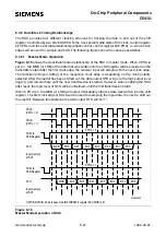
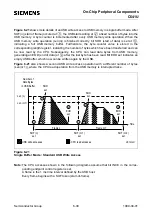
Figure 6-17 shows the clock/data/control relationship of the SSC in slave mode. When SLS is
active (low) and CPHA is 1, the MSB (or LSB) of the data that was written into the shift register will
be provided on the transmitter output after the first clock edge (if the transmitter was enabled by
setting the TEN bit to 1), the receiver input will sample the input data with the next clock edge. The
direction (rising or falling) of the respective clock edge is depending on the clock polarity selected.
In this case (CPHA = 1) the SLS input may stay active during the transmission of consecutive bytes.
When CPHA = 0 and the transmitter is enabled, the MSB (or LSB) of the shift register is provided
immediately after the SLS input is pulled to active state (low). The receiver will sample the input with
the first clock edge, and the transmitter will shift out the next bit with the following clock edge. If the
transmitter is disabled the output will remain in the high impedance state. In this case (CPHA=0),
correct operation requires that the SLS input to go inactive between consecutive bytes.
When SLS is inactive the internal shift clock is disabled and the content of the shift register will not
be modified. This also means that SLS must stay active until the transmission is completed.
If during a transmission SLS goes inactive before all eight bits are received, the reception process
will be aborted and the internal frame counter will be reset. TC will not be set in this case. With the
next activation of SLS a new reception process will be started.
Figure 6-17
Slave Mode Operation of SSC
MSB
MSB
Input Sample
SLS
Input Sample
at SRI
STO
at SRI
(CPOL = 1)
(CPOL = 0)
STO
SCLK
CPHA = 1
CPHA = 0
MCS02441
SCLK
Bit 6
Bit 5
Bit 4
Bit 3
Bit 2
Bit 1
Bit 0
Bit 5
Bit 6
Bit 0
Bit 4
Bit 3
Bit 1
Bit 2
SLS
1) MSB shift first mode is assumed (Bit LSBSM in register SCCMOD is 0)
Summary of Contents for C541U
Page 1: ... 8 LW 026 0LFURFRQWUROOHU 8VHU V 0DQXDO http www siem ens d Sem iconductor ...
Page 7: ......
Page 21: ...Semiconductor Group 2 6 1997 10 01 Fundamental Structure C541U ...
Page 37: ...Semiconductor Group 4 6 1997 10 01 External Bus Interface C541U ...
Page 133: ...Semiconductor Group 6 88 1999 04 01 On Chip Peripheral Components C541U ...
Page 163: ...Semiconductor Group 8 8 1997 10 01 Fail Safe Mechanisms C541U ...
Page 185: ...Semiconductor Group 10 14 1997 10 01 OTP Memory Operation C541U ...

