Semiconductor Group
5-8
1997-10-01
Reset / System Clock
C541U
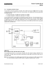
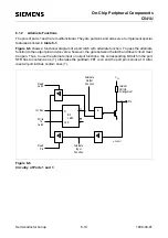
Figure 5-6
On-Chip Oscillator Circuiry
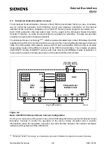
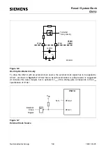
To drive the C541U with an external clock source, the external clock signal has to be applied to
XTAL1, as shown in figure 5-7. XTAL2 has to be left unconnected. A pullup resistor is suggested
(to increase the noise margin), but is optional if
V
OH
of the driving gate corresponds to the
V
IH2
specification of XTAL1.
Figure 5-7
External Clock Source
XTAL2
XTAL1
To Internal
Timing Circuitry
C541U
C
2
C
1
MCD03395
C540U
12 MHz
External
Clock
Signal
V
DD
N.C.
XTAL2
XTAL1
C541U
Summary of Contents for C541U
Page 1: ... 8 LW 026 0LFURFRQWUROOHU 8VHU V 0DQXDO http www siem ens d Sem iconductor ...
Page 7: ......
Page 21: ...Semiconductor Group 2 6 1997 10 01 Fundamental Structure C541U ...
Page 37: ...Semiconductor Group 4 6 1997 10 01 External Bus Interface C541U ...
Page 133: ...Semiconductor Group 6 88 1999 04 01 On Chip Peripheral Components C541U ...
Page 163: ...Semiconductor Group 8 8 1997 10 01 Fail Safe Mechanisms C541U ...
Page 185: ...Semiconductor Group 10 14 1997 10 01 OTP Memory Operation C541U ...

