background image

– 9 –

XL-3500H

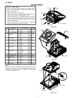
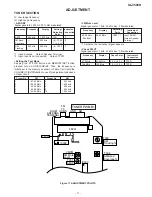
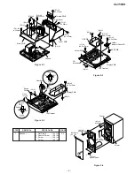
Figure 9-1

Terminal PWB

Rear Panel

Main PWB

Tuner PWB

(G1) x5
ø3 x8mm

(E1) x2
ø3 x10mm

(G2) x2
ø3 x10mm

(G3) x2

(E2) x1

(F2) x1

(D1) x1
ø3 x10mm

(D2) x1

(F1) x1
ø3 x6mm

Chassis

Figure 9-3

Display PWB

CD 
Mechanism

Top Cabinet

Holder PWB

CD PWB

LED PWB

Holder,
Indicator Panel,CD

(J1) x4
ø2.5 x10mm

(H1) x1

(H2) x1

(H2) x1

(H3) x4
ø2.5 x10mm

(K1) x2
ø2.5 x10mm

Display PWB

Gear Box

Switch
PWB

Top Cabinet

(L2) x1

Hook
(L1) x2

Hook
(N1) x3

(M2) x1

(M1) x6
ø2.5 x10mm

Switch
PWB

Switch

Hook
(L1) x2

Pull

Pull

Pull

Pull

,

,

,

Gear Box

Hook
(N1) x3

( A3 ) x2
ø3 x12mm

( A4 ) x4
ø4 x12mm

( A2 ) x2
Special Screw

 Net Frame
( A1 ) x1

( A2 ) x2
Special Screw

Woofer

Tweeter

Figure 9-2

1

Speaker

1. Net Frame ........... (A1) x1

9-4

2. Special Screw ..... (A2) x4
3. Screw .................. (A3) x2
4. Screw .................. (A4) x4

STEP

REMOVAL

PROCEDURE

FIGURE

Figure 9-4

Summary of Contents for XL-3500H

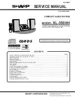
Page 1: ...P W BOARD 32 TROUBLESHOOTING 36 FUNCTION TABLE OF IC 42 LCD SEGMENT 44 PARTS GUIDE EXPLODED VIEW PACKING METHOD FOR U K ONLY SERVICE MANUAL SHARP CORPORATION No S4229XL3500H In the interests of user safety the set should be restored to its original condition and only parts identical to those specified should be used This document has been published to be used for after sales service only The conte...

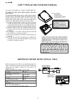
Page 2: ...nit and replacementservicepartshavealreadybeenadjustedprior to shipping 3 No adjustment to the Laser Power should be attempted when replacing or servicing the Pickup 4 Under no circumstances look directly into the Pickup Lens at any time 5 CAUTION Use of controls or adjustments or performance of procedures other than those specified herein may result in hazardous radiation exposure SAFETY PRECAUTI...

Page 3: ... ohms CD digital output optical Input terminals Video Auxiliary audio signal 500 mV 47 kohms Type Compact disc player Signal readout Non contact 3 beam semiconductor laser pickup D A converter 1 bit D A converter Frequency re sponse 20 20 000 Hz Dynamic range 90 dB 1 kHz Frequency range FM 87 5 108 MHz AM 522 1 620 kHz Type 2 way type speaker system 5 cm 2 Tweeter 10 cm 4 Woofer Maximum input powe...

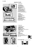
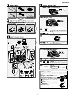
Page 4: ...2 3 4 5 6 7 8 10 12 9 11 1 2 3 4 5 6 7 8 9 10 11 12 Rear panel 1 CD Digital Output Socket 2 Headphone Socket 3 AM Aerial Terminal 4 Aerial Earth Terminal 5 FM 75 Ohms Aerial Socket 6 Cooling Fan 7 Video Auxiliary Audio Signal Input Sockets 8 Speaker Terminals 9 AC Power Input Socket Speaker system 1 Tweeter 2 Woofer 3 Bass Reflex Duct 4 Speaker Terminals Speaker grilles are removable Placing the s...

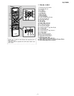
Page 5: ... Reverse Tuning Down Button 20 CD Play Button 21 CD Track Up Button 22 CD Fast Forward Tuning Up Button 23 CD Pause Button 24 CD Stop Button 25 Tuner Preset Down Button 26 Bass Up and Down Buttons 27 Treble Up and Down Buttons 28 RDS Programme Type Traffic Information Search Button 29 RDS ASPM Auto Station Programme Memory Button 30 RDS Display Mode Selector Button Buttons with mark in the illustr...

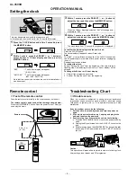
Page 6: ...y to PM 4 Within 1 minute press the PRESET or button to adjust the minutes and then press the MEMORY button The clock starts from 0 second Seconds are not displayed 1 Clear all the programmed contents 2 Perform Setting the clock from the beginning Remote control Test of the remote control Face the remote control directly to the remote sensor on the unit The remote control can be used within the ra...

Page 7: ... indicator FM stereo receiving indicator If trouble occurs When this product is subjected to strong external interference mechanical shock excessive static electricity abnormal supply voltage due to lightning etc or if it is operated incorrectly it may mal function If such a problem occurs do the following 1 Set the unit to the stand by mode and turn the power on again 2 If the unit is not restore...

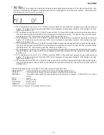
Page 8: ...around the front end of connector remove to protect the optical pickup from electrostatic damage Caution on Disassembly Follow the below mentioned notes when disassembling the unit and reassembling it to keep it safe and ensure excellent performance 1 Take compact disc out of the unit 2 Be sure to remove the power supply plug from the wall outlet before starting to disassemble the unit 3 Take off ...

Page 9: ...CD J1 x4 ø2 5 x10mm H1 x1 H2 x1 H2 x1 H3 x4 ø2 5 x10mm K1 x2 ø2 5 x10mm Display PWB Gear Box Switch PWB Top Cabinet L2 x1 Hook L1 x2 Hook N1 x3 M2 x1 M1 x6 ø2 5 x10mm Switch PWB Switch Hook L1 x2 Pull Pull Pull Pull Gear Box Hook N1 x3 A3 x2 ø3 x12mm A4 x4 ø4 x12mm A2 x2 Special Screw Net Frame A1 x1 A2 x2 Special Screw Woofer Tweeter Figure 9 2 1 Speaker 1 Net Frame A1 x1 9 4 2 Special Screw A2 x...

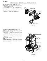
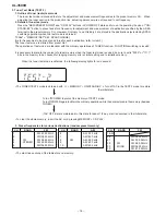
Page 10: ...el CD MECHANISM SECTION See Fig 10 2 Perform steps 1 to 9 of the disassembly method to remove the CD mechanism See page 8 9 1 Remove the mechanism cover paying attention to the pawls A1 x 4 pcs 2 Remove the screws A2 x 2 pcs to remove the shaft A3 x 1 pc 3 Remove the stop washer A4 x 1 pc to remove the gear A5 x 1 pc 4 Remove the pickup unit Note After removing the connector for the optical pickup...

Page 11: ...Hz 5 106 00 MHz 10 1 404 kHz FM Mute Level Signal generator 1 kHz 40 kHz dev FM modulated 1 Adjust so that an output signal appears Check Point Instrument Connection Display Frequency 87 5 MHz 87 5 MHz 2 2 V 0 7 V TP301 108 MHz 108 MHz 7 3 V 1 0 V TP301 Check FM VT Signal generator 1 kHz 40 kHz dev FM modulated 98 00 MHz 98 00 MHz VR351 1 Input SO301 30 dBµV Output Speaker Terminal Instrument Conn...

Page 12: ...e inner periphery Any buttons other than ON STAND BY button are not accepted until the shift of pickup to the inner periphery is completed at this time If PICKUP IN SW ON cannot be detected within 10 seconds the slide motor stops and the following error display appears Press the ON STAND BY button to end the test mode or press the CD STOP button to return to step 1 Any other operations are inhibit...

Page 13: ...s toward the inner periphery while this button is pressed If PICKUP IN is on input is invalid PLAY If focus has been taken shift to step 4 is executed If not acceptance is inhibited STOP Return to step 1 FUNCTION Shift to step 5 If the focus is not received after it has been taken the process returns to step 1 3 Step 3 Mode While the laser keeps lighting CD initialization operation flow proceeds u...

Page 14: ...Press the following buttons in this state to obtain the operations specified below ON STAND BY Test mode and power turned off to shift to the ordinary standby mode FF FWD The pickup slides toward the outer periphery while this button is pressed REW REV The pickup slides toward the inner periphery while this button is pressed If PICKUP IN is on input is invalid PLAY Invalid STOP Return to step 1 FU...

Page 15: ...splayed in hexadecimal numbers The upper two bits which are invalid are displayed as 00 After waiting two seconds operation is shifted to c c Tb is displayed on the left of LCD FTBAST command D482 is transmitted to designate tracking balance adjusting register Then data read by read command SRC2 2 are displayed in hexadecimal numbers After waiting 2 seconds operation is shifted to d d TG is displa...

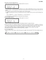
Page 16: ...ching is invalid It is necessary to discard the content of preset memory when the tuner test mode is ended be sure to write 0000 or 1111 bits in the memory to be checked for judging memory error at initial setting and to initialize memory When the tuner test mode is obtained the following display lights for one second The TUNER TEST2 mode is obtained with MEMORY ON STAND BY Turn off AC in the TEST...

Page 17: ...ording to the following procedure to reproduce the timer 1 Set the current time to 1 00 the timer to ON time 1 05 the function to CD and volume to STEP 12 respectively One minute is counted as one second and the timer is reproduced The fade in when playback is started is executed at a rate of one step for 1 sec After completion of fade in the fade out is executed at a rate of one step for 1 sec WA...

Page 18: ... CD OPEN CLOSE The OK NG display of test result is as follows 7 Button input diagnosis Test Mode TEST 6 When the test mode is obtained the following is displayed a POWER ON for function AUX CD lid position is checked CLOSE position Operation proceeds to the next process Position other than CLOSE After the lid moves to CLOSE operation proceeds to the next process b CD lid operation started OPEN ope...

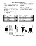
Page 19: ... resistor without any symbol is ohm type resistor Besides the one with Fusible is a fuse type Capacitor To indicate the unit of capacitor a symbol P is used this symbol P means micro micro farad and the unit of the capacitor without such a symbol is microfarad As to electrolyticcapacitor theexpression capacitance withstand voltage is used CH TH RH UJ Temperature compensation ML Mylar type P P Poly...

Page 20: ...C801 40pin STOP PLAY CUE FEI 1 TEI 1 IC801 29pin SBAD 2 TRO 2 IC801 30pin IC801 34pin RFO 3 FMO 3 IC802 22pin IC801 40pin STOP PLAY REVIEW FEI 1 TEI 1 IC801 29pin RFGO 2 TRO 2 IC802 19pin IC801 34pin RFRP 3 FMO 3 IC802 17pin IC801 40pin STOP PLAY TCD 782 TNO 02 PLAYBACK TEI 1 LO 1 IC801 31pin TRO 2 IC801 34pin RO 2 SBAD 3 IC801 30pin 1 2 3 4 6 7 11 15 16 17 IC801 53pin IC801 31pin IC801 31pin IC80...

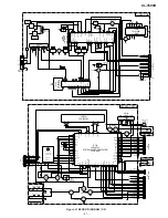
Page 21: ...1 SWITCHING RESET SWITCHING SWITCHING Q701 Q702 Q703 COM0 FAN_DET FAN COM3 SEG0 SEG33 REMOCON P CONT VDD 32 768kHz 8MHz 38 5 4 1 1 100 67 66 65 64 63 62 61 60 59 58 33 57 56 54 53 52 39 48 49 50 32 47 8 4 LCD701 FL DISPLAY TO MAIN PWB REMOTE SENSOR RX701 RESET 23 VSM VLC1 VLC2 VLC3 7 6 5 MMOD VREF VREF VSS 15 24 14 11 SYS_STOP POWER 38 37 13 12 10 55 21 9 X701 X702 OSC1 OSC2 XO XI CLID_SW SW711 71...

Page 22: ...E REG O TRB VG1 VIN1 VO1 VO1 IC803 MM1469PH SPINDLE MOTOR SLED MOTOR PICKUP IN SP SP SL SL PU IN GND FO TR M M CD MOTOR PWB M701 M702 SW702 7 3V 3 3V B1 B6 B2 B4 B5 B6 B5 A C B F E B6 B5 B5 B6 LD MON FOCUS COIL 1 2V 5V TRACKING COIL CD PICKUP UN 23 24 22 21 20 19 18 17 14 26 24 20 19 18 16 35 38 36 37 33 34 31 32 29 28 30 16 15 13 12 11 10 9 8 7 6 5 4 3 2 1 DIGITAL OUT 3 2 1 J801 40 41 FMO DMO 63 ...

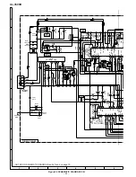
Page 23: ...40203 L CH L CH R CH R CH R CH L CH SPEAKER TERMINAL SO601 HEADPHONES 1 2 3 4 5 9 10 J601 VSS VDD IC401 LC75342M 15 14 13 12 11 10 9 17 18 19 20 21 22 23 24 25 26 27 28 29 16 8 7 6 5 4 3 2 1 CE DI 30 CL LOGIC TUN L CD L TUN R R CH OUT R CH OUT L CH OUT R CH IN L CH IN L CH OUT A_12V NC FUNCTION VOLUME EQUALISER AUX R AUX L CD R MUTE VOLTAGE REGULATOR B6 L IL UP UNIT D_GND MAIN PWB B4 B2 B Q201 Q20...

Page 24: ...M Tracking AM Band Coverage FM Mute Level AM IF AM IF 1 2 3 FM IF FM IF FM IF CH 0 022 1N4148 1N4148 0 022 560P 68K 27P 8P 0 047 0 022 SVC348S 0 001 0 012 0 001 1N4148 1N4148 4 7K 180 0 022 680 0 022 100 16 0 022 82 0 022 2 2µH 68 6 8K 330 2SC380 O 33 680 5 6K 5 6K 8 2K 1mH 10K 33P 3 3 50 0 022 0 022 4 7 25 0 022 0 001 2 7K 456kHz 1 50 0 022 LA1832S 270 0 022 0 022 1K 0 022 10 16 0 022 15P CH 0 00...

Page 25: ...FM SIGNAL 1 2 3 CNP301 P30 5 A TO MAIN PWB A1 FM IF 0 022 0 001 2 7K 456kHz 1 50 56P 1 50 1K 470K 0 027 0 027 6 8K 6 8K KRC104 M 5 6K 5 6K 1 50 1 50 2 2K 1 50 3 3K 2 2 50 0 001 100 10 0 047 270 0 022 0 022 0 022 2 2K 0 01 100µH 5 6K 1K 330P 47K 220P 1 50 10K DZ5 1BSB 100µH 100 10 0 022 390 0 022 390 5 6K KTA1266 GR 5 6K 5 6K 6 8K 47 16 1N4148 10K 4 7K 1 8K 0 022 56K 10K 56K KTC3199 GR 1N4148 0 022...

Page 26: ...308 C B TR TR PO FO GND A E LD VR PD C FFC VIN1 VG1 TRB REG MUTE GND GND GND VG2 VIN2 V02 V02 V03 OPO PO1 PO1 VO3 VIN3 VG3 VCC VCC BIAS VG4 VIN4 V04 V04 VO1 VO1 2 5 7 3 15 13 1 8 9 6 10 11 4 14 12 16 2 5 7 3 15 13 1 8 9 6 10 11 4 14 12 16 SP SP SL SL PU IN GND 5 1 4 3 2 6 4 5 2 6 1 4 3 CD MOTOR PWB C GND PU IN SL SP SP SP PICKUP IN SLED MOTOR SPINDLE MOTOR M 4 6 M 2 M 3 5 1 CD PWB A3 C3A C2A C4A V...

Page 27: ...804 P30 2 B FROM TERMINAL PWB A4 CNP803 P31 8 G TO MAIN PWB A1 CNP808 P31 11 B TO MAIN PWB A1 CNP805 P31 8 G TO MAIN PWB A1 CD SIGNAL 1 1 2 2 3 3 CH CH 100mA 100mA 100mA 33K K 10K 00 10K 22P CH 8 2K 0 1 0 1 100 10 100 10 47 10 0 1 47P 47K 0 015 15K 150K 5 6K 0 0027 0 01 10K 0 033 0 047 470P CH 470P CH 0 033 4 7K 0 047 0 047 TC94A14F 10 16 100 16 10 16 15P 1M 12P 100 10 0 022 0 047 0 047 47 10 0 1 ...

Page 28: ...WB A2 LED PWB A7 LED PWB A6 1 2 1 2 1 2 1 2 CNP701 P30 1 F TO MAIN PWB A1 FL DISPLAY 1 3 2 1 3 2 1 2 3 REMOTE SENSOR 390 390 1N4148 100mA 1N4148 1N4148 100K KRC102 M 3 3 50 1N4148 1K 3 3K 1K 0 01 0 01 KTC3199 GR 1K KTC3199 GR 82 10K DZ3 3BSB 1K 120 10K 100 100 10 560P 10 16 1 5K 1 2K 1 2K 10K 3 9K 4 7K 5 6K 3 9K 47K 10µH 0 1 10K 47K 10K 10K 10K 12K 22P CH 22P CH 1K 47K 47K 1K 1K 1K 1K 1K 1K 1K 1K ...

Page 29: ...SEG22 SEG23 SEG24 SEG25 SEG26 SEG27 SEG28 SEG29 SEG30 SEG31 SEG32 SEG33 REMOCON SYS_STOP POWER CLE SURR P STB P MUTE CD B P CONT DATA ST SD B LIGHT CLID_UP CLID_DW PU IN 38 37 36 35 34 33 32 31 30 29 28 27 26 25 24 23 22 21 20 19 18 17 16 15 14 1 2 1 2 1 2 1 2 3 3 1 2 1 2 FL DISPLAY SWITCH PWB A5 LED PWB A8 CD LID OPEN CLOSE CD LID 1 2 3 1 2 3 P27 12 B TO CD PWB A3 P31 11 F TO MAIN PWB A1 P31 7 8 ...

Page 30: ...AC main voltage CORE TF T1 25A L250V T4A L250V T4A L250V CHASSIS GND CD SIGNAL LINE FILTER 1N5402M 1N5402M 1N5402M 1N5402M 0 1 0 1 0 1 0 1 0 1 0 1 1N4004 1N4004 1N4004 1N4004 10 16 22K 0 022 2SD2012 Y 1N4148 47 820 4700 25 0 0047 KRC107 M KRA102 M KTC3200 GR 100 470 25 DZ8 2BSC 33K 100 25 2SD2012 Y 47 22K 10 16 0 022 KTC3200 GR 2SD2012 Y 47 1N4148 22K 0 022 DZ130A 33K 100 25 470 25 820 100 0 047 0...

Page 31: ...7 2 2 50 0 1 3 9K 0 1 1 50 33 16 100 16 10K 1N4004 1N4004 1N4004 LC75342M 0 1 0 0027 10 16 2 2 50 6 8K 0 0033 0 022 6 8 0 022 0 0033 0 0047 0 0047 0 022 0 022 6 8 10µH 820P 0 01 KRC107 M KTC3199 GR KTA1266 GR KTC3199 GR KTC3199 GR KTC3199 GR KTC3199 GR KTC3200 GR 2SC535 C 3 3K 150 1W 330 1 2W 27K 470K 22K 4 7K 100K 56K 47K 56K 100K 47 50 18K 1N4004 1N4004 1N4004 1N4004 1N4004 1N4148 22K 10K 3 3K 1...

Page 32: ...02 C711 ZD701 R7A7 CNW703 Q701 D721 M702 SW702 CNP703A M701 1 5 10 1 20 25 30 32 33 35 40 45 48 49 50 55 60 64 1 2 3 4 5 6 7 8 9 10 1 5 10 14 15 20 25 28 1 6 7 8 9 10 11 12 13 14 15 16 17 18 19 20 21 22 23 24 25 26 27 28 29 30 31 32 33 34 35 36 37 38 5 1 4 45 50 51 55 60 65 70 75 76 80 85 90 95 100 2 1 1 2 1 1 6 5 1 1 2 2 1 1 3 1 10 2 CD MOTOR PWB C DISPLAY PWB A CD PWB A3 LED PWB A7 SPINDLE MOTOR...

Page 33: ...722 CFW702 C713 Q804 Q806 SW709 SW710 LED704 IC804 R813 Q807 CFW703 RX701 LED703 CFW702A R7A3 CFW703A LED801 D723 CNW701 CNW705 C845 CNP705 CNW706 R845 R783 R759 R751 R737 R786 R789 CNW702 C705 R744 R749 R753 R754 R785 750 CNW707 M801 246 6 SW802 CNP706 1 1 1 16 1 16 3 5 7 9 11 13 15 2 4 6 8 10 12 14 16 5 15 20 24 10 12 13 1 2 3 4 1 5 10 15 16 17 20 25 30 32 33 35 40 45 48 49 50 55 60 64 1 2 3 4 5...

Page 34: ...422 R416 C424 C422 C420 R418 R440 R417 CNP707 R529 R528 CNS301 Q521 X521 C521 L521 Q351 C535 R521 D521 ZD351 C537 C396 C358 C357 R377 C391 R395 R391 R392 R385 R384 L352 C370 C398 CF351 C399 Q360 C352 R382 R386 CF352 D308 CF302 T351 L353 C386 VR351 C385 Q301 X352 R387 L351 CF301 IC302 L342 R336 C393 R343 C394 C380 R380 C348 CFW301 FE301 SO301 D304 D303 L341 D301 D302 T302 C330 R346 VD301 C334 T306 ...

Page 35: ... R101 C417 R105 R202 R218 CNP401 R208 C214 D652 R217 C651 C209 CNP651 IC681 C683 D681 D684 C681 C661 M802 CNP909 CNW909 CFW682 C684 R686 C691 D683 Q683 R886 R885A R885 R883 R884 R881 R880 R882 C880 C881 Q883 D682 D689 R685 CNP701 C665 Q884 Q882 Q881 D881 R887 D688 C688 C689 CNP808 CNP702 CNP881 CNW881 C203 C213 Q203 C215 IC201 R207 C208 D201 C216 R212 Q201 C204 C408 C402 C407 CNP803 C401 C423 C421...

Page 36: ...e used on car CD player or on computer CD ROM drives All rights reserved Unauthorized duplicating broadcasting and renting product is prohibited by law When the CD does not function When the CD section does not operate when the objective lens of the optical pickup is dirty this section may not operate Clean the objective lens and check the playback operation When this section does not operate even...

Page 37: ...he HF output on pin 24 of IC801 in CD TEST MODE STEP 5 Check the procedure HF ERROR Yes No No No No Check the pattern between pin 58 PU_IN of IC701 and CNW704 CNP704 Check the between CNW704 CNP704 and PU IN switch Set ON condition the CD Lid switch Check the procedure in SPINDLE MOTOR CLV SERVO FAILURE No Does the sled motor move No Does the sound heard when the optical pickup move to the selecte...

Page 38: ...t the pin 29 FEI of IC801 when the disc is set Is the waveform shown above input at the pin 30 SBAD of IC801 Yes Yes No No The optical pickup is faulty Check as stated in item FOCUS SERVO SAWTOOTH WAVE FAILURE Yes Check the periphery of IC802 and CNP801 CNW801 Is it normal No Check the pattern between pin 12 of IC802 and pin 30 of IC801 Check the periphery of IC802 and CNP801 CNW801 IC802 is fault...

Page 39: ...etween pins 13 and 16 of CNP801 CNW801 as shown above Yes Check the PWB pattern between CNP801 CNW801 and IC803 No CNP801 CNW801 connection failure or optical pickup failure Yes Spindle motor clv servo failure Is above wave obtained between pins 1 and 2 of IC803 Is following wave output to the pin 41 DMO of IC801 when the CD TEST MODE STEP 3 is changed to STEP 4 No Yes Check the procedure in HF ER...

Page 40: ...50 or 53 of IC801 and the pins 2 or 5 of IC101 No Check the PWB pattern between pin 51 of IC801 and Q808 Yes Is signal of pins 50 and 53 of IC801 output No Check the peripheral parts of IC801 If OK IC801 is faulty Yes The main PWB is faulty Check the periphery of IC802 Check the PWB pattern between pin 11 TEO of IC802 and pins 31 and 32 of IC801 Is it normal Is output obtained at the pins 3 and 8 ...

Page 41: ... the following wave output to the pins 11 TEO of IC802 during track search in normal playback Yes Yes No Check as stated in item SLED MOTOR OPERATION FAILURE No IC801 failure No Check the PWB pattern between pin 34 TRO of IC801 and pin 25 of IC803 Check the PWB pattern between pins 26 and 27 of IC803 and Optical pickup If OK Optical pickup failure Yes Is the above wave output to the pins 31 TEI an...

Page 42: ...L1 Input signal pin 15 NC No CONNECT pin To be open or connected to VSS 16 NC No CONNECT pin To be open or connected to VSS 17 R1 Input signal pin 18 R2 Input signal pin 19 R3 Input signal pin 20 R4 Input signal pin 21 RSEL0 Input selector output pin 22 RIN Volume equalizer input pin 23 RTRE Capacitor connection pin comprising treble band filter 24 RBASS1 Bass band filter comprising capacitor and ...

Page 43: ...14 15 16 17 18 19 20 21 22 23 24 25 26 5 27 28 30 29 1 2 3 4 LVref RVref CCB INTERFACE CONTROL CIRCUIT LOGIC CIRCUIT CONTROL CIRCUIT ROUT RBASS1 RBASS2 RTRE RIN RSEL0 L1 L2 L3 L4 R1 R2 R3 R4 LOUT LBASS2 LBASS1 LTRE LIN LSEL0 VSS CE DI CL VDD NC Vref NC NC TEST Figure 43 BLOCK DIAGRAM OF IC ...

Page 44: ...l4 m4 f4 c5 com4 com4 z2 k1 d1 e1 z3 k2 d2 e2 MHz k3 d3 e3 kHz k4 d4 e4 z4 PinNo 22 23 24 25 26 27 28 29 30 31 32 33 34 35 36 37 38 39 40 41 42 com1 h5 g5 a5 RDS h6 g6 a6 r h7 g7 a7 TP h8 g8 a8 EON com1 com2 j5 n5 p5 b6 j6 n6 p6 b7 j7 n7 p7 b8 j8 n8 p8 PTY com2 com3 l5 m5 f5 c6 l6 m6 f6 c7 l7 m7 f7 c8 l8 m8 f8 TI com3 com4 k5 d5 e5 ST k6 d6 e6 q k7 d7 e7 k8 d8 e8 TA SRS 0 com4 z1 z2 z3 r q z4 1 2 ...

Page 45: ...indrical type without lead wire VC TV Square type without lead wire VC TQ Square type without lead wire VC CY Square type without lead wire VC CZ Square type without lead wire VC J The 13th character represents capacity difference J 5 K 10 M 20 N 30 C 0 25 pF D 0 5 pF Z 80 20 If there are no indications for the electrolytic capacitors error is 20 Resistors VRD Carbon film type VRS Carbon film type...

Page 46: ... 723 VHD1N4148 1 J AA Silicon 1N4148 D801 806 VHD1N4148 1 J AA Silicon 1N4148 D881 VHD1N4004 1 J AB Silicon 1N4004 D891 893 VHD1N4004 1 J AB Silicon 1N4004 LED701 704 VHPLP3052D 1 J AN LED LP3052D LED801 VHPLP99B 1 J AM LED LP99B VD301 VHCSVC348S 1 J AK Variable Capacitance SVC348S ZD351 VHEDZ5R1BSB 1 J AC Zener 5 1V DZ5 1BSB ZD601 VHEDZ130BSA 1 J AC Zener 13V DZ130A ZD602 VHEDZ8R2BSC 1 J AB Zener...

Page 47: ...0 RC GZA106AF1C J AB 10 µF 16V Electrolytic C611 VCKYPA1HB472K J AB 0 0047 µF 50V C651 VCFYFA1HA104J J AC 0 1 µF 50V Thin Film C654 VCFYFA1HA104J J AC 0 1 µF 50V Thin Film 1 C657 660 VCFYFA1HA104J J AC 0 1 µF 50V Thin Film C661 VCKYPA1HB102K J AA 0 001 µF 50V C665 VCFYFA1HA473J J AB 0 047 µF 50V Thin Film C681 VCFYFA1HA473J J AB 0 047 µF 50V Thin Film C683 RC GZV228AF1C J AG 2200 µF 16V Electrolyt...

Page 48: ... 6W R385 VRD ST2CD562J J AA 5 6 kohms 1 6W R386 VRD ST2EE331J J AA 330 ohms 1 4W R387 VRD ST2CD562J J AA 5 6 kohms 1 6W R391 392 VRD ST2EE391J J AA 390 ohms 1 4W R393 VRS CY1JB102J J AA 1 kohm 1 16W R395 VRD ST2CD473J J AA 47 kohms 1 6W R401 402 VRS CY1JB102J J AA 1 kohm 1 16W R405 406 VRS CY1JB273J J AA 27 kohms 1 16W R407 408 VRS CY1JB272J J AA 2 7 kohms 1 16W R415 VRS CY1JB102J J AA 1 kohm 1 16...

Page 49: ...in CNP909 QCNCM998BAFZZ J AC Plug 2Pin CNS301 QCNCW010PAWZZ J AE Socket 14Pin CNW102 QCNWN0447SJZZ J Connector Ass y 2Pin CNW103 QCNWN0446SJZZ J Connector Ass y 2Pin CNW104 QCNWN0447SJZZ J Connector Ass y 2Pin CNW401 QCNWN0395SJZZ J Connector Ass y 3 3Pin CNW701 QCNWN0436SJZZ J Connector Ass y 7 7Pin CNW702 QCNWN0400SJZZ J Connector Ass y 13 13Pin CNW703 QCNWN0437SJZZ J Connector Ass y 3 3Pin CNW7...

Page 50: ...08 XEBSF25P08000 J AA Screw ø2 5 8mm 609 XEBSF30P10000 J AA Screw ø3 10mm 610 XHBSD30P06000 J AA Screw ø3 6mm 611 XHBSF30P06000 J AA Screw ø3 6mm 612 XJBSD30P06000 J AA Screw ø3 6mm 613 XJBSD30P08000 J AA Screw ø3 8mm 614 XJBSD30P10000 J AA Screw ø3 10mm 615 XJBSF30P10000 J AA Screw ø3 10mm 616 XHBSD20P03000 J AA Screw ø2 3mm 617 LX HZ0240AFFD J AB Screw Special 618 LX WZ9004SJSA J Washer 5 5mm 61...

Page 51: ...XL 3500H A B C D E F G H 1 2 3 4 5 6 Figure 6 CD MECHANISM EXPLODED VIEW 6 308 1 703 304 703 303 302 704 301 M701 702x2 306x2 SW702 M702 PWB C 308 3 308 2 308 701 305 307x2 ...

Page 52: ...3x6 220 242 LCD701 221 231 241 217 229 230x2 230x2 220 234 230 216 228 232 236 236 236 236 215 205 237 225 616 240 617x4 619x2 606x2 606 606x6 606x4 610x5 609x4 607x4 606 609x2 608 601x4 615x2 616x2 611 609x4 613x3 614x3 604 601 612 603 611 601x2 239 222 249 247 248 612 223 201 233 244 246 246 2 246 4 246 3 246 1 246 5 246 6 M801 PWB B1 PWB A1 PWB A8 PWB A6 PWB A7 PWB A2 PWB B2 CD MECHANISM PWB A5...

Page 53: ... SP604 R CH SP601 L CH SP602 R CH SP603 L CH SP604 R CH Tweeter Tweeter Capacitor Capacitor 2 2µF 50V SP601 L CH SP602 R CH Woofer Woofer Red Red Black Black 907 901 906 902x2 905 909x4 SP601 SP602 SP603 SP604 908x2 903 3 903 2x2 903 2x2 904 1 904 903 904 3 904 2 910x2 910x2 903 1 ...

Page 54: ...8 Packing Add Right SPAKA0117SJZZ 9 Packing Case SPAKC0211SJZZ 10 Sleeve Carton Speaker SPAKS0007SJZZ 11 Polyethylene Bag Speaker SPAKZ0039SJZZ 13 19 11 6 10 7 8 12 22 1 3 5 4 2 14 20 15 16 17 9 18 12 Pad Accessories SPAKZ0063SJZZ 13 Polyethylene Bag Unit SPAKZ0064SJZZ 14 Polyethylene Bag Accessories SSAKA0009SJZZ 15 Register Card TCADN0003SJZZ 16 Operation Manual TINSE0087SJZZ 17 Quick Guide TINS...

Page 55: ...XL 3500H MEMO ...
Page 56: ...ma 739 0192 Japan Printed in Japan COPYRIGHT 2002 BY SHARP CORPORATION ALL RIGHTS RESERVED No part of this publication may be reproduced stored in a retrieval system or transmitted in any from or by any means electronic mechanical photocopying recording or otherwise without prior written permission of the publisher ...

Reviews: