background image

XE-A302U

DIAGNOSTIC PROGRAM

– 13 –

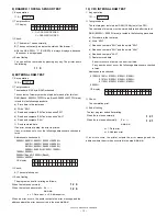
8) DRAWER 1 OPEN & SENSOR TEST

1

Key operation

110 

3


2

Test procedure

3

Check:

A) The drawer 1 opens normally.

B) The sensor correctly indicates the status of the drawer 1.

*

On the XE-A302U, “C” (CLOSED) is always displayed, because
the sensor is not equipped.

4

End of testing

You can exit the test mode by pressing any key. The printer prints
the following.

1 1 0

9) EXTERNAL RAM TEST

1

Key operation

120 

3


2

Test procedure

The standard 512 Kbyte RAM is checked.

The contents of memory must be stored before and after this test.

RAM (Bank0: 08000H~7FFFFH area, Bank2: 28000H~2FFFFH area)
is tested in the following procedure:

a) Store data in the test areas

b) Write  “00H”

c) Read and compare “00H” and then write”55H”

d) Read and compare “55H” and then write “AAH”

e) Read and compare “AAH”

f) Restore stored data

If an error occurs at a step, the error is printed.
If any error does not occur, the following addresses are checked in
turns.

Addresses to be checked:

08000H, 08001H, 08002H, 08004H, 08008H, 

08010H, 08020H, 08040H, 08080H, 
08100H, 08200H, 08400H, 08800H,
09000H, 0A000H, 0C000H, 10000H,

18000H, 20000H,
28000H (Bank0), 28000H (Bank2),
30000H, 40000H

3

Check:

A) The completion print.

4

End of testing

The program ends after printing as follows:

When an error occurs, the printer outputs the error message and the
address where the error has occurred in the area 

*****

.

10) CPU INTERNAL RAM TEST

1

Key operation

121 

3


2

Test procedure

The test program tests internal RAM (10 Kbytes) of the CPU.

The contents of memory must be stored before and after this test.

RAM (00400H ~ 02BFFH area) is tested in the following procedure.

a) Store data in the test area.

b) Write “00H”

c) Read and compare “00H” and then write “55H”

d) Read and compare “55H” and then write “AAH”

e) Read and compare “AAH”

f) Restore stored data

If an error occurs at a step, the error is printed.

If any error does not occur, the following addresses are checked
in turns.

Addresses to be checked:

01000H, 01001H, 01002H, 01004H, 01008H,

01010H, 01020H, 01040H, 01080H,

01100H, 01200H, 01400H, 01800H,

02000H

3

Check:

The completion print.

4

End of testing

If an error occurs, the printer outputs the error message and the

address where the error has occurred in the area 

*****

.

When the test ends normally:

1 2 0

When the test end abnormally: Ex – ~ –

*****

1 2 0

x = 1: Data error, x = 2: Address error

RCPT/PO

D R A W E R

P G M

X

OP display

X : O = DRAWER OPENED

C = DRAWER CLOSED

1

RCPT/PO

R A M

P G M

OP display

1 2 0

The test program ends after printing.

When the test ends normally:

1 2 1

When the test ends abnormally:

Ex – ~ –

1 2 1

*****

x = 1: Data error

x = 2: Address error

RCPT/PO

R A M

C P U

P G M

OP display

1 2 1

Summary of Contents for XE-A302

Page 1: ...lished to be used for after sales service only The contents are subject to change without notice XEA302USME ELECTRONIC CASH REGISTER MODEL XE A302 U and A version CHAPTER 1 SPECIFICATIONS 1 CHAPTER 2 OPTIONS 4 CHAPTER 3 MASTER RESET AND PROGRAM RESET 4 CHAPTER 4 HARDWARE DESCRIPTION 5 CHAPTER 5 DIAGNOSTIC PROGRAM 11 CHAPTER 6 IPL FROM EP ROM 15 CHAPTER 7 CAUTION TO BE USED WHEN CONNECTING THE RS 2...

Page 2: ... E J PRINT 56 45 34 23 12 1 46 35 24 13 2 57 67 47 36 25 14 3 58 68 48 37 26 15 4 59 69 49 38 27 16 5 60 70 50 39 28 17 6 61 71 51 40 29 18 7 62 72 52 41 30 19 8 63 53 42 31 20 9 73 64 54 43 32 21 10 74 65 55 44 33 22 11 75 66 CLK 2 4 6 1 3 5 AUTO ESC 2 DEPT RCPT PO PLU SUB FOR RA TAX CONV TAX1 SHIFT TAX2 SHIFT CH1 CH2 MDSE SBTL CHK TM SBTL 1 2 RFND VOID CA AT 1 2 3 4 5 6 7 8 9 0 00 CL KEY TOP DES...

Page 3: ...t in a safe place Power save mark When the cash register goes into the power save mode the power save mark decimal point lights up Function message display area Item labels of departments and PLU subdepartments and function texts you use such as 1 and CASH are displayed When an amount is to be entered or entered AMOUNT is dis played When an amount is to be entered is displayed at the numeric entry...

Page 4: ...E 6 million lines used to high quality thermal paper Paper end sensor Set up Cutter No Near end sensor No Paper roll dimension 57 5 m 0 5mm in width Max 80mm in diameter Paper quality High quality thermal paper paper thickness 0 06 to 0 08mm 0 167 4 75 4 75 48 288 dots print area max 24 characters units mm 57 5 0 5 Paper dimension Model name of the drawer box SJ423 Size 420 W x 426 D x 114 H mm 16...

Page 5: ...ter reset operation 2 PROGRAM RESETTING INITIALIZATION This resetting resumes the initial program without clearing memory This resetting can be operated at below sequence in PGM mode Note In case power failure occurs when the machine has no battery attached to it the master reset operation is automatically per formed after the power has been restored NO NAME PARTS CODE PRICE RANK DESCRIPTION 1 The...

Page 6: ...Fh 256KB x 2 FLASH ROM CS0 area BANK 0 address 80000h FFFFFh 256KB Moves to Bank 1 when rewritten using EPROM Reserve CS0 area BANK 6 address 80000h FFFFFh 256KB I O CS3 area BANK 0 address 04000h 07FFFh 16KB 00000h 00400h 02C00h 04000h 08000h 28000h 30000h 40000h 60000h 80000h C0000h FFFFFh Bank 0 Bank 1 Bank 2 Bank 3 Bank 4 Bank 5 Bank 6 Bank 7 BR1 0 0 1 1 0 1 1 0 BR2 1 1 1 1 0 0 0 0 BR0 1 1 0 1...

Page 7: ... 5VDC m 5 When paper empty is detected printing is terminated However when paper empty is detected during printing 15 dot lines from detection of paper empty can be printed 3 5 PLATEN OVER When signals are sampled in the frequency of 1ms or less and open state is detected twice continuously it is judged as platen over If the head is conducted under the platen over state the thermal head life may b...

Page 8: ...A2 P73 27 O P73 DRAWER 1 L Out L DRAWER DRIVE SIGNAL P20 72 O A0 A0 Out L P74 26 O P74 ER1 H Out L RS 232 ER1 P21 71 O A1 A1 Out L P75 25 I P75 CD1 In RS 232 CD1 P22 70 O A2 A2 Out L P76 24 I P76 CS1 In RS 232 CS1 P23 69 O A3 A3 Out L P77 23 I P77 DR1 In RS 232 DR1 P24 68 O A4 A4 Out L P80 22 O P80 BUZZER L Out L P25 67 O A5 A5 Out L P81 21 O P81 MOTOR L In Printer winding motor P26 66 O A6 A6 Out...

Page 9: ... Keyboard 04001h 04003h PORT PIN No I O Pin name Function PORT PIN No I O Pin name Function BYTE 8 I BYTE Connected to VDD Vcc 62 Vcc Connected to VDD CNVss 9 I CNVss Connected to VDD Vss 64 Vss connected to GND RESET 12 I RESET AVss 96 AVss Connected to GND Xout 13 O Xout OPEN Vref 98 Vref Connected to VDD Vss 14 Vss Connected to GND AVcc 99 AVcc Connected to VDD Xin 15 I Xin connected to Spectra...

Page 10: ... from COM Data from the PC is written to flash ROM through the COM port Max 38 4 kbps 8 DRAWER The machine has a 1 channel of drawer port No open sensor is provided The driving time for the DRAWER solenoid are as follows 50ms max 45ms min CPU STO ST1 ST2 ST3 ST4 ST5 ST6 ST7 ST8 ST9 MODE P90 SRV PGM Time REG MGR X1 Z1 X2 Z2 KEYBD Others P91 PF HEAD UP PE DRAWER OPEN RS 232 CI1 KEYBD 1 Normal Keyboa...

Page 11: ...ltage The RESET signal is generated under the following conditions 1 When the mode key switch is set from SRV to another position except for OFF position 2 When the power is turned on after 5sec or more from turning off the power and the VCC reaches 5V 3 When the mode key switch is set from OFF position to another posi tion except for SRV position and VCC reaches 5V If the OFF time is within 5sec ...

Page 12: ...DE 1 Key operation 101 3 2 Test procedure 3 Check 4 End of testing You can exit the test mode by turning the mode switch to a position other than the PGM mode The printer prints as follows 1 0 1 Code Description 1 100 Display buzzer test 2 101 Key code 3 102 Printer test 4 104 Keyboard test 5 105 Mode switch test 6 106 Printer sensor test 7 107 Clock display test 8 110 Drawer 1 open sensor test 9 ...

Page 13: ...arted 5 MODE SWITCH TEST 1 Key operation 105 3 2 Test procedure The above X must be read in the correct order If the contact is open 9 will be displayed 3 Check The display during testing and the content of the completion print 4 End of testing 6 PRINTER SENSOR TEST 1 Key operation 106 3 2 Test procedure Check the status of the paper end sensor and head up sensor 3 Check the following 4 End of tes...

Page 14: ...rogram ends after printing as follows When an error occurs the printer outputs the error message and the address where the error has occurred in the area 10 CPU INTERNAL RAM TEST 1 Key operation 121 3 2 Test procedure The test program tests internal RAM 10 Kbytes of the CPU The contents of memory must be stored before and after this test RAM 00400H 02BFFH area is tested in the following procedure ...

Page 15: ...ormally E 1 3 0 ROM Model name Version RCPT PO R O M F L A S H P G M OP display 1 3 0 RCPT PO T M P G M OP display Display 1 6 0 V R F P G M OP display 1 6 0 V P T E S T P G M OP display 1 6 0 End of testing OUTPUT INPUT ER RS DR CI CD CS OFF OFF OFF OFF OFF OFF OFF ON OFF OFF ON ON ON OFF ON ON OFF OFF ON ON ON ON ON ON Completion print RS TEST OK 500 Error print RS TEST NG ERxx 500 xx Contents o...

Page 16: ...ime ECR looks like inactive but ECR waits the ROM data from PC IPL software on PC 7 Copy the following files in PosUtilityTool3 into the hard disk of PC Postool3 exe A302u ROM 8 Boot Postool3 exe 9 Push Add Files in the screen 10 Select the ROM DATA file File name A302u ROM 11 By pushing Send in the screen the ROM data is sent from PC to ECR The address counter is shown on PC and counts up 12 Afte...

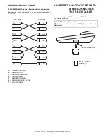
Page 17: ...RTS REQUEST TO SEND DCD DATA CARRIER DETECTOR CTS CLEAR TO SEND CHAPTER 7 CAUTION TO BE USED WHEN CONNECTING THE RS 232 CABLE When connecting the RS 232 cable to the XE A302 be sure to observe the following condiiton SD 3 SD RD CTS RD 2 6 8 3 2 6 8 5 5 SG RTS 7 DCD 1 DTR 4 DSR 7 1 4 CTS SG RTS DCD DTR DSR 9PIN D SUB 9PIN D SUB Use RS 232 cable with core of accessories This is a necessary to suppor...

Page 18: ... 15 16 17 18 19 20 21 22 23 24 25 26 27 28 29 30 79 78 77 76 75 74 73 72 71 70 69 68 67 66 65 64 63 62 61 60 59 58 57 56 55 54 53 52 51 50 49 48 47 46 45 44 43 42 41 40 39 38 37 36 35 34 33 32 31 D7 D8 D6 D5 D4 D3 D2 D1 D0 AN7 AN6 AN5 AN4 AN3 AN2 AN1 AVSS AN0 VREF AVCC SIN4 SOUT4 CLK4 TB4IN TB3IN SOUT3 SIN3 CLK3 BYTE CNVSS XCIN XCOUT RESET XOUT VSS XIN VCC NMI INT2 INT1 INT0 TA4IN U TA4OUT U TB3IN...

Page 19: ...RAM HY628400ALLT 1 2 3 4 5 6 7 8 9 10 11 12 13 14 15 16 32 31 30 29 28 27 26 25 24 23 22 21 20 19 18 17 A18 A16 A14 A12 A7 A6 A5 A4 A3 A2 A1 A0 D0 D1 D2 GND VCC A15 A17 WR A13 A8 A9 A11 RD A10 CS D7 D6 D5 D4 D3 R87 0 C57 10uF 50V C54 0 1uF R89 10K S1 IPL SW SSS312 2 1 3 R86 0 IC10 PAL16V8H 1 2 3 4 5 6 7 8 9 10 11 12 13 14 15 16 17 18 19 20 CLK I0 I1 I2 I3 I4 I5 I6 I7 I8 GND OE I9 I O0 I O1 I O2 I ...

Page 20: ... Q4 LE C83 0 1uF Q3 KRC111S B E C R94 10K CN4 R LCD CN 1 2 3 4 5 6 IC14 74HC273 3 4 7 8 13 14 17 18 11 1 2 5 6 9 12 15 16 19 D1 D2 D3 D4 D5 D6 D7 D8 CLK CLR Q1 Q2 Q3 Q4 Q5 Q6 Q7 Q8 FB3 JUMPER C134 10uF 16V C66 0 1uF C67 0 1uF CN6 DR CN 2Pin 5046 03A 1 2 3 IC17 BA00ASFP 2 1 4 5 6 3 R99 12K D21 1SS355 A K Q2 2SD2212 B E C C82 0 1uF R96 5 6K R100 10K IC21 74HC245 1 2 3 4 5 6 7 9 10 8 20 19 18 17 15 1...

Page 21: ...5 A K R167 0 R116 4 7K C87 10u F 50V R19 1K Q6 2SK2731 G D S CN12 PRINTER CN 1 2 3 4 5 6 7 8 9 10 11 12 13 14 15 16 17 18 19 20 21 22 23 24 25 26 R111 20K R114 10K Q8 KRC111S B E C C86 0 1uF Q7 2SK2731 G D S C91 10u F 50V C88 47uF 50V C85 0 1uF R112 10K D6 1SS355 A K CN7 MO TOR CN 1 2 D18 1SS355 A K R115 30KF C133 22u F 16V FB5 0 EFCB322513TS R109 47K Q4 2SD2212 B E C IC22 LB1838M 1 2 13 6 9 7 14 ...

Page 22: ...P2 VBAT2 1 R133 100 CN9 Mn B AT CN 1 2 D7 FMB G24H A K R141 10K PS CN 1 2 R143 560 IC25A BA10393F 3 2 1 8 4 R119 18 0KF Q12 KRC106S B E C ZD4 UDZ5 1B A K D13 RB551 30 A K R134 1KF R127 3KF Q11 KRA106 S B E C R136 3 9K CN8 PS CN 1 2 TP1 VO 1 R132 220 R122 5 6K L2 180uH Ch ock POWER TRANS3 100V 50 Hz 60Hz F5 T2 0A 250V R142 6 2KF D12 1SR159 200 A K R118 10 FUSE R R120 3 3KF R139 56K ZD3 UDZ5 1B A K ...

Page 23: ...TK A 1 2 3 4 5 6 7 8 9 10 11 12 13 14 15 16 17 18 19 20 21 22 23 24 25 26 CN31 JST 27FMN B YK A 1 2 3 4 5 6 7 8 9 10 11 12 13 14 15 16 17 18 19 20 21 22 23 24 25 26 27 A B C D 8 7 6 5 4 3 2 1 1 2 3 4 5 6 7 8 D C B A A B C D 8 7 6 5 4 3 2 1 1 2 3 4 5 6 7 8 D C B A A B C D 8 7 6 5 4 3 2 1 1 2 3 4 5 6 7 8 D C B A A B C D 8 7 6 5 4 3 2 1 1 2 3 4 5 6 7 8 D C B A 6 7 M T53II Printer I F ...

Page 24: ...0 0 1uF IC27 HIN211 12 14 15 16 7 6 20 21 8 5 26 22 19 24 13 17 2 3 1 28 9 4 27 23 18 25 11 10 C1 C1 C2 C2 T1IN T2IN T3IN T4IN R1OUT R2OUT R3OUT R4OUT R5OUT EN V V T1OUT T2OUT T3OUT T4OUT R1IN R2IN R3IN R4IN R5IN SHDN VCC 10 R155 10K R156 10K R157 10K FB9 R158 10K F7 T500mA 250 V R151 C119 1000pF R160 10K FB10 FB7 FB11 FB8 C115 0 1uF R150 FB12 C113 10u F 50V SP1 1 3 2 R152 R153 C120 1000pF FB13 D1...

Page 25: ...XE A302U CIRCUIT DIAGRAM AND PWB LAYOUT 24 PWB LAYOUT MAIN PWB LAYOUT A side ...

Page 26: ...XE A302U CIRCUIT DIAGRAM AND PWB LAYOUT 25 B side ...

Page 27: ...03 August Printed in Japan t COPYRIGHT 2003 BY SHARP CORPORATION All rights reserved Printed in Japan No part of this publication may be reproduced stored in a retrieval system or transmitted In any form or by any means electronic mechanical photocopying recording or otherwise without prior written permission of the publisher ...

Reviews: