background image

TM200

1ADJUSTMENTS, PERFORMANCE CHECK, AND FIRMWARE UPGRADE

2 – 34

CONFIDENTIAL

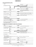
8. MP3 CANNOT BE PLAYED.

9. VIDEO/VOICE RECORDER PLAYBACK IS IMPOSSIBLE.

Speaker

Not defective.

Is Ringer Volume set to “Silent”?

ancel “S

C

ilent”. Is sound produced?

Go to the section “Video/Voice Recorder playback is impossi-
ble.” 

Is output of the video and voice recorder normal?

Are keypad tones and ring tones normal?

Go to the section “Speaker does not work.” 

Insert an SD card with MP3 files recorded on a normal unit. 
Do they play?

Not defective.

Is the SD card recognized?

Go to the section “SD (Memory) card is not recognized.” 

Is the signal sent to IC103 pin 60?

Parts between IC103 pin 60 and IC105 pins 14 & 13 are 
defective or soldered improperly.

IC103 is defective.

Hands free kit (headset)

(The following procedure applies to both monaural and stereo headsets.)

Is sound normally produced from Speaker?

Go to the section regarding Speaker.

Replace the hands free kit. Is sound produced?

Hands free kit is defective.

Go to “Hands free kit (monaural headset)” in the section “No 
voice is heard from the earpiece.” 

YES

YES

NO

NO

NO

YES

YES

NO

YES

NO

NO

YES

YES

NO

NO

YES

YES

NO

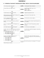
Speaker

Are keypad tones and ring tones normal?

Go to the section “Speaker does not work.” 

In Playback window, does playback start normally and the 
capacity bar change?

IC101 or IC106 is defective.

Not defective.

Is Ringer Volume set to "Silent"?

Cancel “Silent”. Is sound produced?

Is the signal sent to IC103 pin 60?

Parts between IC103 pin 60 and IC105 pins 14 & 13 are 
defective or soldered improperly.

IC103 is defective.

Hands free kit (headset)

* If R-ch is the only channel of stereo headset that does not send signals, see “Hands free kit (stereo headset)” in the section 
   “No voice is heard from the earpiece.”
Replace the hands free kit.
Is the signal sent?

Hands free kit is defective.

In Playback window, does playback start normally and the 
capacity bar change?

IC101 or IC106 is defective.

Not defective.

Is Ringer Volume set to "Silent"?

Cancel "Silent". Is sound produced?

Go to “Hands free kit (monaural headset)” in the section “No voice is heard from the earpiece.”

NO

YES

NO

YES

YES

YES

NO

NO

YES

NO

YES

NO

NO

YES

YES

YES

NO

NO

Summary of Contents for TM200

Page 1: ...l to those specified should be used Caution Risk of explosion if battery is replaced by an incorrect type dispose of used batteries according to the instruction SERVICING CONCERNS CHAPTER 1 GENERAL DESCRIPTION 1 Specifications 1 1 2 Names of parts 1 2 3 Operation manual 1 2 CHAPTER 2 ADJUSTMENTS PERFORMANCE CHECK AND FIRMWARE UPGRADE 1 SHARP Program Support Tool SPST 2 1 2 Test points 2 25 3 Troub...

Page 2: ...inals on the electric board microphone vibrator earpiece and speaker When handling these parts wear fingerstalls Should you touch these parts clean them with a soft dry cloth Always wear fingerstalls when handling a shield case on the electric board Otherwise oxidation may occur causing handset performance deterioration 7 The FPC is a precision device Handle it carefully to prevent any damages 8 D...

Page 3: ...epth 262k 1 colours Resolution QVGA 240 x 320 dots External display Type 1 06 inch Semi Transmissive system LCDs Colour depth 65k colours Resolution 96 x 64 dots Connections Bluetooth TM SD memory card slot 2 Earphone MIC USB Ver 1 1 RF connector Sound Chords 40 chord polyphonic ringtones Format AAC MP3 SMAF MIDI i melody WAVE AMR Contacts list Phonebook 500 entries Messaging SMS Text message MMS ...

Page 4: ...262 4 785 450 4 811 420 Licensed under U S Patent 4 558 302 and foreign counterparts CP8 PATENT SD logo is a trademark T9 Text Input is licensed under one or more of the following U S Pat Nos 5 818 437 5 953 541 5 187 480 5 945 928 and 6 011 554 Australian Pat No 727539 Canadian Pat No 1 331 057 United Kingdom Pat No 2238414B Hong Kong Sandard Pat No HK0940329 Republic of Singapore Pat No 51383 Eu...

Page 5: ...xplorer to execute the setup exe file on the CD ROM 2 The SPST TM200 setup wizard appears Follow the installation instructions 3 After the installation is complete shortcuts to SPST are created on the desktop and under the Start Programs TM200 menu Start SPST from the shortcuts 2 3 STARTING UP Connect TM200 to an operable serial port of the PC with the supplied data cable Make sure that the batter...

Page 6: ... calibration check RF Test Refer to 4 6 RF test tool User Password Reset Refer to 4 7 Password reset Performance check adjustment Refer to 4 8 Performance check and adjustment mode release Refer to 4 9 mode release Exit End SPST Parts Temperature adjustment Camera Temperature adjustment Battery Main display flicker adjustment White defect correction TH101 u F u u TH701 F u u u Main display unit u ...

Page 7: ...ngs 4 Communication starts 5 The following appears when you select Yes in step 3 and MEPLOCK data exists Click Yes to restore the data 6 After the handset is turned on the initialization is complete 4 2 USER DATA BACK UP SPST saves all the data stored on the handset 1 Set the COM port on the SPST initial screen and click User Data Back up 2 Specify the file name in the following dialog box and cli...

Page 8: ...he software and how to connect handset to a PC 1 Installing uninstalling the software Installing the software Note Downloader is installing uninnstalling simultaneously with SPTP 1 Double click the setup exe icon in TM200 Install E folder 2 The Setup Wizard is activated Click the Next button 3 A location to install the software appears To install in the default location click the Next button To ch...

Page 9: ...system While installing the upgrading tool in Windows 98 98 SE or ME a message may appear prompting to restart the operating system In this case restart your operating system follwoing the instruction Even if the message does not appear restart your operating system after the installation On Windows 98 if you start the upgrading tool without restarting the operation system the following message ma...

Page 10: ...C 2 Connect the cable to handset 3 The photo below shows handset connected to a PC B Using Communication Box 1 Connect a PC to Communication Box via a serial cable 2 Connect the AC charger to Communication Box and then plug it into the outlet All SET POWER SW on Communication Box must be turned off 3 Connect the conversion connector to Communication Box Cables Connect the conversion connector in t...

Page 11: ...ding When rewriting MOT files using the upgrading tool do not connect the AC charger to the cable If you connect the cable connected to the AC charger to handset charging starts and the MOT file rewrite operation is interrupted All SET POWER SW on Communication Box must be turned off If handset is connected with SET POWER SW turned on charging starts and the MOT file rewrite operation is interrupt...

Page 12: ...ppears alerting you a possible error Click the OK button to proceed and click the Cancel button to change the value You can shorten time for the MOT rewrite operation by selecting a smaller value for Wait Time Example Time to rewrite two MOT files at a time At the default setting 3 seconds rewrite time is approximately 40 minutes If the value is set to 1 the rewrite time will be reduced to approxi...

Page 13: ...ard disk first 4 Rewriting a MOT file Click the Start Loading Flash button to start rewriting 1 Press Power Button appears When using a cable for upgrading Hold down the Power key When using the Communication Box Turn on Communication Box SW from No 10 down to No 1 turn on only the handsets you are using 2 Keep Pressing Power Button appears When using a cable for upgrading Hold down the Power key ...

Page 14: ...e default Wait Time 3 seconds increase the value Consequently this will increase the time to complete the rewrite operation 5 Checking the value of SUM When the rewrite operation is completed a confirmation message appears with SUM SUM also appears on handset When using a cable for upgrading After 8 seconds SUM disappears When using Communication Box When SET POWER SW is turned off SUM disappears ...

Page 15: ...elect a COM port connected to the PC cable 6 RAM Loader not responding to Commands No response from Loading loader Start over the rewrite operation 7 RAM Loader responding Parameter Error Information sent from the PC is illegal Reinstall the upgrading tool Start over the rewrite operation 8 RAM Loader responding Flash Error XXXX Failed to initialize FLASH ROM in XXXX Start over the rewrite operati...

Page 16: ...nitial screen returns 4 5 4 RF performance check Insert SIM card 1 Apply 4 V using a stabilized power supply and turn on the handset 2 Start RF calibration check on SPST and click Calibration 3 When initialization is complete click OK 4 Apply 4 V using a stabilized power supply and turn on the handset After the handset enters Standby mode lower the voltage to 3 7 V 5 Make sure the handset is in th...

Page 17: ... starts 8 The following message appears during the check Press the keys 1 2 3 and Send again and click OK 9 Make sure the terminal display is In Call and click OK 10 RF performance check is complete Click Save As and name the file to save the result Click OK to exit The following will be displayed in case of failure See the attachment 2 for troubleshooting 11 Click OK 12 The initial screen returns...

Page 18: ...CL5 44 Mod_spectrum 800 124CH PCL5 45 Mod_spectrum 800 37CH PCL11 46 Mod_spectrum 600 37CH PCL11 47 Mod_spectrum 400 37CH PCL11 GSM900 Tx 48 Mod_spectrum 250 37CH PCL11 49 Mod_spectrum 200 37CH PCL11 50 Mod_spectrum 200 37CH PCL11 51 Mod_spectrum 250 37CH PCL11 52 Mod_spectrum 400 37CH PCL11 53 Mod_spectrum 600 37CH PCL11 54 Mod_spectrum 800 37CH PCL11 55 Mod_spectrum 800 37CH PCL19 56 Mod_spectru...

Page 19: ...99CH PCL0 139 Mod_spectrum 800 512CH PCL0 Band Sending Receive No Item to be inspected Channel PCL DCS Tx 140 Mod_spectrum 600 512CH PCL0 141 Mod_spectrum 400 512CH PCL0 142 Mod_spectrum 250 512CH PCL0 143 Mod_spectrum 200 512CH PCL0 144 Mod_spectrum 200 512CH PCL0 145 Mod_spectrum 250 512CH PCL0 146 Mod_spectrum 400 512CH PCL0 147 Mod_spectrum 600 512CH PCL0 148 Mod_spectrum 800 512CH PCL0 149 Mo...

Page 20: ... 230 Burst Power 512CH PCL0 231 Burst Power 810CH PCL0 Band Sending Receive No Item to be inspected Channel PCL PCS Tx 232 Burst Power 661CH PCL5 233 Burst Power 661CH PCL15 234 Frequency Error 661CH PCL0 235 Frequency Error 512CH PCL0 236 Frequency Error 810CH PCL0 237 Phase Error RMS 661CH PCL0 238 Phase Error RMS 512CH PCL0 239 Phase Error RMS 810CH PCL0 240 Phase Error Peak 661CH PCL0 241 Phas...

Page 21: ...810CH PCL0 315 Switch_Spectrum 1200 810CH PCL0 316 Switch_Spectrum 1800 810CH PCL0 317 Switch_Spectrum 1800 661CH PCL5 318 Switch_Spectrum 1200 661CH PCL5 319 Switch_Spectrum 600 661CH PCL5 320 Switch_Spectrum 400 661CH PCL5 321 Switch_Spectrum 400 661CH PCL5 322 Switch_Spectrum 600 661CH PCL5 323 Switch_Spectrum 1200 661CH PCL5 324 Switch_Spectrum 1800 661CH PCL5 Band Sending Receive No Item to b...

Page 22: ... port to which Data Cable is connected 5 Press the Initialize Read Data button 6 The figre shown below appears wait a few seconds 7 Click OK to proceed 4 6 3 Tests 1 BAND Select Channel Select a band and a channel to test Settings are applied to all tests Procedure 1 Select a band GSM900 DCS or PCS 2 Select or enter a channel using Channel bar or Input box Hook Hook Hook PWB Hook Hook Hook Red PC ...

Page 23: ...he handset receives burst signals in this test PCL bar TX frequency of selected channels Current PCL Read only TX ON OFF button This indicator appears during burst transmission Data patterns PCL GSM900 Tolerance dBm 5 33 2 dB 6 31 3 dB 7 29 3 dB 8 27 3 dB 9 25 3 dB 10 23 3 dB 11 21 3 dB 12 19 3 dB 13 17 3 dB 14 15 3 dB 15 13 3 dB 16 11 5 dB 17 9 5 dB 18 7 5 dB 19 5 5 dB PCL DCS PCS Tolerance dBm 0...

Page 24: ...nuous sine wave without modulation with the frequency as follows Frequency of the measured channel 67 708kHz Ex channel GSM 37ch 3 the result 942 467708 MHz Power 110 to 10 dBm 2 BCCH signal of the measured channel Power 110 to 10 dBm Result When the handset is properly calibrated the error between Esti mated Power and Measured Power is less than 3dB 4 6 4 Termination Turn off the handset to ensur...

Page 25: ...t recognized in 3 Troubleshooting 4 8 7 Vibrator test Click to vibrate the handset Click OK to exit If a failure occurs see 5 Vibrator does not work in 3 Trouble shooting 4 8 8 Melody test A message describes test items Click Yes to proceed and No to exit The order of the test items speaker 3 hands free 3 hands free stereo 3 speaker analog melody 4 8 9 Audio test The following appears Select a tes...

Page 26: ...0 cm from a fluorescent light and adjust the value to minimize flicker on the display with the b and c buttons Click Save and confirm that the main display does not flicker Fine adjustment for DC voltage between display electrodes 4 8 15 External display contrast adjustment Click the External display contrast adjustment button The following screen appears Trouble found by SPST 1 Handset microphone...

Page 27: ... sensor appear as black points in the dis play even when a captured image is completely white display is all white Perform black defect correction to eliminate errors in these pixels 1 Requirements Desk top type of fluorescent lamp Black defect correction sheet Illuminance meter 2 Procedure 1 Cover the camera section with the black defect correction sheet as shown in Figure 96 2 Check the distance...

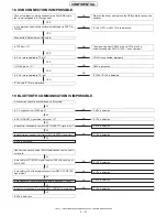
Page 28: ... tests of Bluetooth USB communication Check them according to the following instructions 5 1 USB Connect TM200 and a PC with a USB cable Check that TM200 is recognized as a device If the USB driver for TM200 SHARP GSM GPRS USB Driver is not installed on the PC Found New Hardware window appears and Found New Hardware Wizard starts the handset is recognized 5 2 BLUETOOTH Connect TM200 to the network...

Page 29: ...702 R706 R514 R1205 R515 R1206 R516 R131 R132 R133 R135 CN501 R136 CN502 R713 CN503 R714 R138 R520 R139 R522 R523 R718 R719 C103 C106 C107 R720 C108 R722 R723 R147 R149 R727 C110 X101 R150 C114 C115 R151 R153 R156 R158 C504 R540 R159 C505 R542 C507 R543 C120 R544 R545 R546 R160 R161 R162 R164 C510 R741 R742 C51 2 C707 R744 R168 R745 C516 R747 R553 R749 C136 R173 R750 R751 C139 R752 C716 C522 R753 ...

Page 30: ...TP528 DGND TP165 VT 2 75V TP535 Reserved TP166 VUSB TP536 ManufactUre Specific TP167 VRTC 1 8V TP537 CHGIN TP168 VBACK 3V TP801 VTCXO 2 9V TP169 VSIM 2 85V TP802 VRF 2 9V TP170 VMEM 2 8V MAINPWB B REARSIDE R211 R212 R221 R222 R223 R224 R226 R227 R228 R230 R231 R232 R233 R234 R235 TP101 TP102 TP103 TP104 R251 TP105 TP107 TP108 TP109 TP113 TP118 TP119 TP502 TP503 TP506 TP120 TP121 TP123 TP124 TP125 ...

Page 31: ...705 R723 R727 R728 R729 R730 R732 R733 R734 R735 R736 R737 R738 C701 C702 C703 R740 C704 R741 C705 C706 R742 C707 R743 C708 C709 R746 R747 R748 R749 C710 C711 C712 C713 C714 R750 C717 C718 C719 R756 C720 C721 C722 C723 C724 C725 C726 C727 C728 C729 C730 C731 C732 C733 C734 C735 C736 C737 C738 C739 C742 C744 C745 C746 C747 C748 C749 C750 C751 C752 C753 C754 C755 C756 C757 C758 C759 C760 C761 D701 D...

Page 32: ... supply for camera 8 V TP710 Backlight Flash LED TP727 Power supply for camera 15V TP711 Backlight 1 TP728 VDD2 3V TP712 CAMCLK TP729 VBAT TP713 13MHzCLK TP733 VDD1 1 8V TP714 VLCD 1 8V TP734 RECIVER_OUT TP715 Terminal for LCDC adhesion check 1 TP735 RECIVER_OUT TP716 Terminal for LCDC adhesion check 2 TP738 VBAT TP717 VOUT External Display LCD PWB REAR SIDE TP701 TP702 TP705 TP706 TP707 TP708 TP7...

Page 33: ...tart after restart 5 level stack memory IC101 and IC106 are defective Program code of 5 level stack memory IC101 is garbled YES NO YES NO NO YES YES NO NO YES Connect a battery of 4 0 V or more Is 3 6 V or more applied to BATT terminal TP520 Battery terminals are defective connector terminal is dirty or soldering is improper Is the voltage 1 2 V or lower on SENSE terminal TP506 The battery is defe...
Page 34: ... YES YES NO NO YES NO YES NO YES NO YES NO YES YES NO Hands free kit headset The following procedure applies to both monaural and stereo headsets Replace the hands free kit Is the signal sent Hands free kit is defective C104 R112 and V101 are defective Is 0 7 1 8 V applied to JK101 pin 2 Is 0 7 1 8 V applied to TP120 Is 2 4 2 5 V applied to TP176 R122 is defective Is 2 4 2 5 V applied to IC103 pin...

Page 35: ...in 60 R124 is defective Is the voltage 0 V on R192 IC106 pin 89 side Jack JK101 is defective or the jack plug is in a poor contact with hands free kit Handset mode is set Is approx 1 2 V applied to IC103 pin 60 IC103 is defective IC103 or IC106 is defective YES NO YES NO YES NO NO YES NO YES YES NO YES NO YES NO YES NO YES NO NO YES NO YES Hands free kit stereo headset Option The headset cannot be...

Page 36: ...tween Q108 FET 1pin and 2pin Is 0V applied between Q108 FET 3pin and 4pin IC116 or IC103 is defective IC103 is defective TH101 or R148 is defective IC115 or R281 or R282 or R283 or C229 is defective Q101 or R286 is defective NO NO NO YES YES YES YES Are vibrator terminals in contact with the land Are terminals and the land clean Vibrator is deformed and defective When vibrator terminals and the la...

Page 37: ...ad Tones is set to Off When Ringer Volume is set to Silent Voice Recorder playback sound is not produced Playback sound of Video and MP3 can be heard by increasing the volume during playback Are speaker terminals in contact with the land Speaker is defective Is the impedance between speaker terminals approx 8 ohms Speaker is defective Is the signal sent to TP701 TP702 or speaker contact pad Speake...

Page 38: ... defective Go to Hands free kit monaural headset in the section No voice is heard from the earpiece YES YES NO NO NO YES YES NO YES NO NO YES YES NO NO YES YES NO Speaker Are keypad tones and ring tones normal Go to the section Speaker does not work In Playback window does playback start normally and the capacity bar change IC101 or IC106 is defective Not defective Is Ringer Volume set to Silent C...

Page 39: ...ean Is back light FPC properly inserted to CN705 Clean back light FPC and insert it again Does it turn on Not defective Is 3 6 V applied between TP710 and TP705 Is 3 6 V applied between TP710 and TP706 Is 3 6 V applied between TP710 and TP707 Is 3 6 V applied between TP710 and TP711 Back light FPC is defective Are C735 C791 C733 C738 C730 C731 R708 and R707 in good appearance and mounted properly ...

Page 40: ...upplied GSM900 bands IC803 pin 16 DCS1800 PCS1900 bands IC803 pin 14 IC802 is defective Is frequency signal supplied to pin 1 of FL905 IC803 is defective Is frequency signal supplied to pin 1 of J801 FL905 is defective J801 is defective Receiver 70 dBm input Is frequency signal supplied GSM900 bands IC801 pins 9 10 DCS1800 band IC801 pins 6 7 PCS1900 band IC801 pins 3 4 IC801 is defective Is frequ...

Page 41: ... Power is not turned on Is 3 0 0 1 V supplied from LCD_RST R749 Are R746 C736 C751 CN701 and CN703 good in appear ance and mounted properly R746 C736 C751 CN701 and CN703 are defective or mounted improperly Is 3 0 V 0 1 V applied to CN704 pins 34 37 and 38 Are R736 R738 C774 and C775 good in appearance and mounted properly CN704 R737 R738 C774 and C775 are defective or mounted improperly Is 3 0 0 ...

Page 42: ... 0 1 V supplied from LCD_RST CN703 pin 27 and C751 IC704 C736 C751 and R749 are defective or mounted improperly Is R222 good in appearance and mounted properly R222 is defective or mounted improperly Are C755 C756 and C757 good in appearance and mounted properly Is electric potential normal at both ends of C755 C756 and C757 Are rectangular waves sent C755 rectangular wave of approx 3 V C756 recta...

Page 43: ...s defective Camera relay FPC is broken Is 15 V applied to TP727 CN701 is defective Camera relay FPC is broken Is 15 V applied to pin 48 of camera module YES NO NO YES NO YES NO YES NO YES NO YES NO YES NO YES NO YES NO YES Is 8 Is 8 V applied to TP726 V applied to pin 1 of camera module CN701 is detective Camera relay FPC is bloken Is signal properly sent from CAMCK TP712 IC704 and FL701 is defect...
Page 44: ...d in appearance and mounted prop erly IC106 is defective Replace R163 R249 or C218 Is 2 85 V supplied from CN104 pin 27 Are R163 R249 and C218 good in appearance and mounted properly CN104 or SD SIM FPC is defective IC106 is defective YES NO YES NO NO NO YES YES NO NO YES YES NO NO YES YES NO NO YES YES Is 2 85 V supplied from CN104 pin 28 Is the SD card checked for operation Use an SD card that h...
Page 45: ...03 or IC106 is defective IC106 and IC701 are defective NO YES NO YES NO YES NO YES NO YES NO YES A connection cannot be established via Bluetooth Is 3 V supplied from IC505 pin 5 IC505 is defective Is R514 RESET signal side always at H IC106 is defective Is waveform periodically sent from R516 UARTTX signal side IC506 is defective Is waveform periodically sent from R547 UARTRX signal side IC506 is...

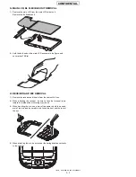
Page 46: ...Disengage the pawls and remove the cabinet B unit 3 Remove the speaker from the cabinet B unit When installing the speaker fit the speaker projection a with the concaved rib section C VIBRATING MOTOR REMOVAL 1 Open the display section Remove the screw cover and remove the special screw When removing or installing the special screw use the exclusive tool When tightening the screws follow the tighte...

Page 47: ...ctor with the main LCD PWB silk section as the refer ence When attaching the submersion sheet b attach it inside the bump area When attaching the PWB unit rotate the main PWB and the LCD PWB 180 degrees in the arrow direction to wind the flat cable 2 Remove the camera shield case unit from the main LCD PWB unit and remove the camera flexible unit Disengage the pawl and remove the sub LCD unit Disc...

Page 48: ...ess TAB a H RECEIVER AND MIC REMOVAL 1 Remove the receiver and the mic from the cabinet A C unit When attaching the receiver be sure to face the terminal a tip toward the inside without covering over the rib When handling the mic use a pair of tweezers to hold the periph eral of the mic and be careful not to touch the front and the rear of the mic When attaching the mic be sure to set the spring d...

Page 49: ...CONFIDENTIAL CONFIDENTIAL CHAPTER 4 DIAGRAMS 1 Block diagram Main TM200 DIAGRAM 4 1 TM200 DIAGRAM 4 2 ...

Page 50: ...Loop filter 90deg Shift PGA Test Connector VBAT 900 1800 1900 90deg Shift SAW Filter 4 PCS RX DCS RX SYNTHEN D SYNTHDATA D SYNTHCLK D 1 2 Srial data interface VRF TCXOEN D VBAT LNA LNA LNA GSM 900 RX BS2 BS4 VTCXO RX Line Control Line TX Line BS1 BS2 BS3 DPD Voltage Regulator D Digilal A Analog PA APC SAW Filter IC802 PF08141B IC803 FL902 J801 IC801 HD155155 IC804 TCX801 FL903 1800 1900 900 TM200 ...

Page 51: ...35 LCD controler Power souceIC BD6020 BD6030 LTC3205 Backlight LED Flash LED CCD camera I F I F LCD 15V 1 8V 8V 3 0V Series regulator 㧗1 8V 㧗3 0V VDT OVP AC charger Constant voltage Constant current AD6535 Lithium ion Battery pack reg External headphone External Microphone 1 Sound signal system USB Analog UART UART Serial I F CN BU7880 Interface SW LDO M ON OFF YM762 AD6535 Typhoon Key LED Light V...

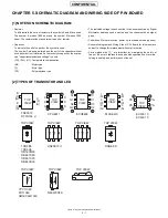
Page 52: ...assis with no signal given Conditions SIM card inserted power on in stand by mode opened Schematic diagram and Wiring Side of P W Board for this model are subject to change for improvement without prior notice Parts marked with are important for maintaining the safety of the set Be sure to replace these parts with specified ones for main taining the safety and performance of the set 2 TYPES OF TRA...

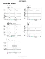
Page 53: ... talking C812 IC801 26pin 1 2 3 4 STOP Channel_62 Gain 62dB SniffOff 5 6 7 STOP RF Test Tool Rx test GSM900 Band Channel 62 SYSNTHEN Stand by IC801 29pin SYNTHCLK Stand by IC801 30pin SYNTHDATA Stand by IC801 32pin 8 9 10 11 STOP RF Test Tool Tx test GSM900 Band BS1E talking C872 IC803 6pin BS2E talking C871 IC803 7pin BS3 talking C870 IC803 8pin BS4 talking C863 IC802 16pin 8 9 10 11 STOP RF Test...

Page 54: ...g C870 IC803 8pin BS4 talking C863 IC802 16pin 8 9 10 11 STOP RF Test Tool Rx test PCS1900 Band BS1E talking C872 IC803 6pin BS2E talking C871 IC803 7pin BS3 talking C870 IC803 8pin BS4 talking C863 IC802 16pin 13MHz IN Point R261 To Digital Base Band LSI Pin142 13MHz OUT Point R166 from Digital Base Band LSI Pin84 32 768KHz IN Point R152 To Digtal Base Band LSI Pin49 12 13 14 ...

Page 55: ... CIRCUIT DIAGRAM AND PWB LAYOUT 5 4 CONFIDENTIAL DCLK Point R759 on LCDC_PCB To LCD Unit pin26 VSYNC Point C760 on LCDC_PCB To LCD Unit pin28 TCXOEN Point IC804 pin 1 From Analog Base Band LSI Pin 2 15 16 17 ...

Page 56: ...P 470K R151 0 R138 C103 0 1 USB_CHG_EN 620 NU R119 0 R169 470K R168 LED108 U GM1BC35370 NU USB_CURRENT_CTL 0 R161 C157 47000P TP107 0 R226 C109 10080MAB C198 0 1 MODESEL2 470K R189 X101 C0065 C112 47P 470K R160 CHGIN 5 2V VBAT TEMP1 VBUS_IN 5 0V L103 Z0315 620 R109 LED106 YPY1105C AUDIO_IN C186 0 1 L101 HM102 C179 0 1 MODESEL3 VSIM 2 85V C165 0 1 VAPP TP108 0 R203 27 R179 0 R172 RECIVER_OUTP C153 ...

Page 57: ...CONFIDENTIAL CONFIDENTIAL 8 7 6 5 4 3 2 1 A B C D 1 2 3 4 5 6 7 8 D C B A RF PART MAIN TM200 CIRCUIT DIAGRAM AND PWB LAYOUT 5 7 TM200 CIRCUIT DIAGRAM AND PWB LAYOUT 5 8 ...

Page 58: ...3 SW517 KARBON R0 3 SW504 KARBON R0 3 SW511 KARBON R0 3 SW518 KARBON R0 3 SW510 KARBON R0 3 SW505 KARBON R0 3 SW522 KARBON R0 3 SW519 KARBON R0 3 KEYPADCOL 0 4 KEYPADROW 0 4 POWONKEY USB_DET CN501 AA002 1 2 3 TP501 R501 TP503 TP502 TP505 TP504 TP506 BATTYPE 00 R540 18K R509 C510 1 6 3V 0 R507 D503 RB160M C507 1 6 3V 47K R511 USB_CHG_EN IC505 XC620930 1 2 3 4 5 C516 1 VBAT BT_POWER_ON BT_RESET BT_P...

Page 59: ...7 1 16V C744 1 16V C753 0 1 C748 1 6 3V TP713 TP710 TP711 TP720 C761 10P C766 0 01 0 R716 VLCD 1 8V C728 1 6 3V C729 1 6 3V C727 C732 0 1 C739 0 1 C734 0 1 0 R717 C759 10P C760 10P C758 10P C751 100P TP712 12 R738 CHANGE VRS CZ1JD120J TP714 TP709 C718 1 6 3V 470K R732 R715 TP734 TP735 TP732 TP733 VBAT_L Battery VBAT Battery ZD703 RSB6R8S Not ZD704 RSB6R8S Not C711 47P C712 47P C722 1 6 3V TP702 TP...

Page 60: ...0 R139 R522 R523 R718 R719 C103 C106 C107 R720 C108 R722 R723 R147 R149 R727 C110 X101 R150 C114 C115 R151 R153 R156 R158 C504 R540 R159 C505 R542 C507 R543 C120 R544 R545 R546 R160 R161 R162 R164 C510 R741 R742 C512 C707 R744 R168 R745 C516 R747 R553 R749 C136 R173 R750 R751 C139 R752 C716 C522 R753 C717 R179 C142 C143 C144 C723 C724 C149 R186 R187 R188 FS501 FS502 C156 C158 C159 C1875 C1876 C187...

Page 61: ...LED103 LED104 TP158 LED105 LED106 LED107 LED108 L101 LED109 L102 TP160 TP161 TP162 TP163 LED110 TP164 LED111 TP165 LED112 TP166 LED113 TP167 LED114 TP168 LED115 TP169 LED116 LED117 LED118 LED119 TP170 TP171 TP172 TP173 LED120 TP174 LED121 LED122 TP176 TP177 TP178 TP179 TP180 TP181 TP182 TP183 TP184 TP185 TP186 TP187 TP188 SW501 SW502 SW503 SW504 SW505 SW506 SW507 SW508 SW509 R103 R104 R105 R106 R1...

Page 62: ...37 R738 C701 C702 C703 R740 C704 R741 C705 C706 R742 C707 R743 C708 C709 R746 R747 R748 R749 C710 C711 C712 C713 C714 R750 C717 C718 C719 R756 C720 C721 C722 C723 C724 C725 C726 C727 C728 C729 C730 C731 C732 C733 C734 C735 C736 C737 C738 C739 C742 C744 C745 C746 C747 C748 C749 C750 C751 C752 C753 C754 C755 C756 C757 C758 C759 C760 C761 D701 D702 D703 C766 C769 D709 C770 D710 C771 C772 C773 C774 C7...

Page 63: ...TP702 TP705 TP706 TP707 TP708 TP709 TP710 TP711 TP712 TP713 TP714 TP715 TP716 TP717 TP720 TP721 TP722 TP723 TP724 TP725 TP726 TP727 TP728 TP729 TP732 TP733 TP734 TP735 TP738 TP739 TA701 TA702 L704 R703 CN701 TH701 C715 C716 C740 C741 C743 C788 C789 Q LCD PWB_REAR ...

Page 64: ...04 TO MAIN PWB A REAR SIDE 5 14 8 D CN705 TO MAIN PWB A REAR SIDE 5 14 8 B CN701 MAIN PWB A FRONT SIDE 5 13 3 G TO MAIN PWB A REAR SIDE 5 14 12 G TO MAIN PWB A REAR SIDE 5 14 9 G SOLDER SOLDER BACK LIGHT FPC PWB C B TO MAIN PWB A REAR SIDE 5 14 12 G E A TO KEY PWB B REAR SIDE 5 28 11 A C TO KEY PWB B FRONT SIDE 5 27 4 A D CN102 TO KEY PWB B REAR SIDE 5 28 9 A CN104 TO KEY PWB B REAR SIDE 5 28 11 G...

Page 65: ...E 1 2 3 4 5 IC115 PIN NO VOLTAGE 1 2 3 4 0V 0V Not used 0V IC116 PIN NO VOLTAGE 1 2 3 4 0V 0 14V 0V 0 14V IC505 PIN NO VOLTAGE 1 2 3 4 5 3 69V 0V 0V Not used IC804 PIN NO VOLTAGE 1 2 3 4 5 6 2 96V 3 80V 2 96V 2 89V 0V 2 89V Conditions SIM card inserted power on battery 3 7V in stand by mode opened Measuring instrument Digital multimeter Unmeasurable IC506 PIN NO VOLTAGE 1 2 3 4 5 6 7 8 9 10 11 12 ...

Page 66: ... High Z High impedance 27 A21 Input Address input NOR Flash Smartcombo RAM 2 28 SC2 CE2 Input Sleep state input Smartcombo RAM 2 29 DQ13 Input Output Data input output NOR Flash Smartcombo RAM SRAM Command Address and Data input output Smartcombo Flash 30 DQ6 Input Output Data input output NOR Flash Smartcombo RAM SRAM Command Address and Data input output Smartcombo Flash 31 DQ4 Input Output Data...

Page 67: ... input NOR Flash Smartcombo RAM SRAM 72 A1 Input Address input NOR Flash Smartcombo RAM SRAM 73 SC1 CE1 Input Chip enable input Smartcombo RAM 1 74 NC Not used 75 NC Not used 76 NC Not used Pin No Terminal name Input Output Description of terminal 77 SF WP Input Write protect input Smartcombo Flash 78 SF CE Input Chip enable input Smartcombo Flash 79 A5 Input Address input NOR Flash Smartcombo RAM...

Page 68: ...n supply 2 75 3 3 V 49 BSOFS Output Baseband serial port output framing signal 50 BSDI Input Baseband serial port data input 51 VBAT2 Input Analog baseband regulator input 52 NC_G16 Not used 53 CSDO Output Control serial port data output 54 CSDI Input Control serial port data input 55 VBAT2 Input Analog baseband regulator input 56 VABB Output Analog baseband supply 57 ASM Input Advanced state mach...

Page 69: ...d for power supply 143 AGND0 Thermal ground for power supply 144 AGND0 Thermal ground for power supply 145 AGND0 Thermal ground for power supply 146 AGND0 Thermal ground for power supply 147 AGND0 Thermal ground for power supply 148 AGND0 Thermal ground for power supply Pin No Terminal name Input Output Description of terminal Pin No Terminal name Input Output Description of terminal 1 CLKI Input ...

Page 70: ...upply 1 7 1 9 V VCORE 32 KEYPADCOL 3 Output KEYIN signal output 3 33 KEYPADCOL 2 Output KEYIN signal output 2 34 GPIO_39 Output USB PU control for interface IC 35 GPIO_37 Input Interrupt input from analog BB 36 GPIO_34 Output UART_TXD for Bluetooth module 37 ADD 4 Output Processor address bus 4 38 ADD 2 Output Processor address bus 2 39 GND Ground 40 KEYPADROW 0 Input KEYIN signal input 0 41 VEXT ...

Page 71: ...ss bus 23 109 GND Ground 110 VEXT Input SIM power supply 2 4 3 3 V VINT 111 GND Ground 112 GPIO_4 Output UART_CTS for Bluetooth module 113 GPIO_2 Output USB charge current control 114 GPIO_3 Input UART_RTS for Bluetooth module Pin No Terminal name Input Output Description of terminal 115 DATA 2 Input Output Processor data bus 2 116 DATA 0 Input Output Processor data bus 0 117 DATA 5 Input Output P...

Page 72: ...PO_4 Output Mode select 1 for interface IC 182 GPO_7 Output Bluetooth module power ON OFF control 183 GPO_16 Output Band select 1 for RF BS1 184 GPO_17 Output Band select 2 for RF BS2 185 NHWR NUSB Output Processor high write strobe 186 GPO_19 Output Mode select 3 for interface IC 187 NLWR NLSB Output Processor low write strobe 188 NWAIT Input Processor wait input 189 NRESET Input System reset inp...

Page 73: ...le 4 ECO Input High speed low consumption selector switch 5 VOUT Output Output Pin No Terminal name Input Output Description of terminal 1 A Input Signal input 2 B Input Signal input 3 GND Ground 4 Y Output Logic value output 5 VCC Input Power supply 5 1 2 VOUT NB 4 3 Bandgap Reference Thermal Protection VIN CONT GND 5 4 2 VDD CE GND VOUT ECO VREF CURRENT LIMIT 3 1 1 A B GND VCC TOP VIEW Y 2 3 5 4...

Page 74: ...S NC TXANAIN RXANAOUT USBD RXD CPU_USB_D CPU_USB_D REG33 PU15 PUEA GND3 RXANAIN TXANAOUT MODESEL3 BCNT BDATA UART_CTS 19 15 16 17 MODE 0 1 2 ON MODE 3 5 OFF CPUVDD CPUVDD CPUVDD CPUVDD DEC H ON L OFF CPUVDD CPUVDD CPUVDD CPUVDD CPUVDD CPUVDD MODE 0 1 2 OFF MODE 3 5 ON MODE 0 2 3 OFF MODE 1 5 ON MODE 0 2 3 5 OFF MODE 1 ON MODE 0 2 3 5 L MODE 1 H MODE 0 2 3 5 L MODE 1 H MODE 0 2 3 5 L MODE 1 H MODE ...

Page 75: ...nput Output For factory use only Not used 33 PIO2 Input Output General purpose I O 34 PIO0 Input Output General purpose I O Pin No Terminal name Input Output Description of terminal 1 INB Input Input B 2 INA Input Input A 3 GND Ground 4 OUT Y Output Output Y 5 VCC Power supply 1 IN B IN A GND TOP VIEW VCC OUT Y 2 3 5 4 Pin No Terminal name Input Output Description of terminal 1 VSS Ground GND 2 VI...

Page 76: ...al Display is active when CS_B is Low 23 VDDIO IO Power supply 3 0 V 2 7 V 3 3 V 24 LCDINT Output External interrupt signal Starting varies when interruption occurs 25 GTDIO_B Output MPEG4ASIC internal core power cut signal Low is active 26 VDDIO IO Power supply 3 0 V 2 7 V 3 3 V 27 SUBDB1 Input Output Data bus for External display 28 BDATA 5 B5 Output Display panel B output signa 29 BDATA 5 B4 Ou...

Page 77: ... ground Pin No Terminal name Input Output Description of terminal 84 VDDCORE CORE Power supply 1 8 V 1 6 V 2 0 V 85 CAMCK Output Clock for camera operation 86 GDATA 1 G1 Output Display panel G output signal 87 GDATA 0 G0 Output Display panel G output signal 88 RDATA 5 R5 Output Display panel R output signal 89 RDATA 4 R4 Output Display panel R output signal 90 VDDCORE CORE Power supply 1 8 V 1 6 V...

Page 78: ...signal 2 for 4 wire serial IF General purpose PORT output default 131 BUFOFF_B Input Buffer Gated switching signal for I O through current prevention High when Host_IF signal is activated 132 VDDIO IO Power supply 3 0 V 2 7 V 3 3 V 133 DUMMY2 Dummy 2 134 SE_LD3 PORT6 Output Load signal 3 for 4 wire serial IF General purpose PORT output default Not used 135 VDDIO IO Power supply 3 0 V 2 7 V 3 3 V 1...

Page 79: ...pand RED Pallet BLUE Pallet CDE DCS_B DA 1 0 EXCS_B 3 0 ADDRESS DECODE SE_DI PORT7 Memory Interface 72bit BS_DATA 71 0 SEL Buffer 18bitx4 Buffer 18bitx4 Some MHz to 68 MHz PLL Dividing Oscillation circuit Current consumption is decreased in a standby mode Some MHz to 33 MHz Approx 16 128 MHz External MPEG4_ASIC External CAMERA_DSP 4 wire SO PO 6 bit x 4 Available for magnification function CPU sys...

Page 80: ...ositive TxVCO output for GSM 22 VCCIQ Input VCC for IQ modulator 23 IOUT IIN Input Output Positive output input of I channel modulator 1 VCONT 500K 320K VIN VOUT Bandgap Reference Control Circuit Over Heat Over Current Protection 2 GND 3 NP 5 4 24 IOUTB IINB Input Output Negative output input of I channel modulator 25 QOUT QIN Input Output Positive output input of Q channel modulator 26 QOUTB QIN ...

Page 81: ...nal circuit node Do not externally connect 28 NC Internal circuit node Do not externally connect 29 NC Internal circuit node Do not externally connect 30 GND Internally connected to the package base 31 DCS PCS OUT RF output for the DCS PCS bands This is a 50Ω output The output matching circuit and DC block are internal to the package 32 GND Internally connected to the package base 33 NC Internal c...

Page 82: ...erface chip select 33 RESET Input Hardware reset 34 VCC Logic power 35 GND Ground 36 GND Ground 37 VDC Analog power 38 VDC Analog power 39 COM2 COM control for CS 40 VCLAMP Output Voltage for CS output 41 VSS2 Output DC DC converter output 42 VSS1 Output DC DC converter output 43 NC Not used 44 VDD2 Output DC DC converter output 45 C5 Booster capacitor connection terminal 46 C5 Booster capacitor c...

Page 83: ...input selection terminal L Built in oscillation 25 VDD VEE Logic system power supply terminal 26 VREG Output Output terminal for generating constant voltage 27 VOUT Output Built in step up circuit output terminal 28 CAP1 Output Booster capacitor con nection terminal 29 CAP1 Output Booster capacitor con nection terminal 30 CAP2 Output Booster capacitor con nection terminal 31 CAP2 Output Booster ca...

Page 84: ...pan 2004 December Printed in Japan t COPYRIGHT 2004 BY SHARP CORPORATION All rights reserved Printed in Japan No part of this publication may be reproduced stored in a retrieval system or transmitted In any form or by any means electronic mechanical photocopying recording or otherwise without prior written permission of the publisher ...

Reviews: