background image

HR-MB3

8 – 8

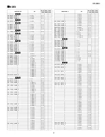
IC500 RH-IXA069AWZZ: 256MB SDRAM (IXA069AW)

In this unit, the terminal with asterisk mark (*) is (open) terminal which is not connected to the outside.

Pin No.

Terminal Name

Function

40*

N.C./RFU

No connection.

41

VSS

Ground.

42

DQ8

Data inputs/outputs are multiplexed on the same pins.

43

VDDQ

Data output power.

44, 45

DQ9, DQ10

Data inputs/outputs are multiplexed on the same pins.

46

VSSQ

Data output ground.

47, 48

DQ11, DQ12

Data inputs/outputs are multiplexed on the same pins.

48

DQ1, DQ2

Data inputs/outputs are multiplexed on the same pins.

49

VDDQ

Data output power.

50, 51

DQ13, DQ14

Data inputs/outputs are multiplexed on the same pins. 

52

VSSQ

Data output ground.

53

DQ15

Data inputs/outputs are multiplexed on the same pins.

54

VSS

Ground.

54

DQ7

Dynamic power path management set point. (account for scale factor)

Summary of Contents for HR-MB3

Page 1: ... 1 CHAPTER 2 ADJUSTMENTS 1 TEST Mode 2 1 2 Error History Display 2 2 3 Error Code List 2 3 4 Updating the firmware 2 4 5 Replacing the HDD unit 2 4 6 Downloading the latest firmware 2 4 CHAPTER 3 MECHANISM BLOCKS 1 Caution on diassembly 3 1 CHAPTER 4 DIAGRAMS 1 Block diagram 4 1 CHAPTER 5 CIRCUIT DESCRIPTION 1 Notes on schematic diagram 5 1 2 Types of transistor 5 1 3 Waveforms of circuit 5 2 4 Vo...

Page 2: ...ch is higher than the conventional lead solder by 40 C and as it has poor solder wettability you may be apt to keep the soldering bit in contact with the PWB for extended period of time However Since the land may be peeled off or the maximum heat resistance temperature of parts may be exceeded remove the bit from the PWB as soon as you confirm the steady soldering condition Lead free solder contai...

Page 3: ... 5 mW 5 mW maximum output level 32 ohms Battery life Up to 20 hours of continuous playback by fully charged re chargeable Lithium ion battery PC interface USB 1 1 2 0 Notes A combination of sampling frequency and bit rate dif fers depending on audio format Continuous playback At 128 kbps in MP3 format earphone output 0 1 mW 0 1 mW backlight not set to Always equalizer set to Flat Actual battery li...

Page 4: ...tandby and display the version of the firmware and Parameter To enter test mode press these keys in the following order MENU key RIGHT key DOWN key UP key RIGHT key Press for 2 seconds RETURN key Test mode ends and the TOP screen appears Check that Parameter is updated and EXIT is displayed Use UP key and DOWN key to select EXIT Change Exit or Default load Update the specified area of Parameter ME...

Page 5: ...o Yes Error history appears Error history content appears Use UP key and DOWN key to scroll The latest history to be displayed in most significant Up to 10 error history records are displayed History clear mode ENTER key ENTER key ENTER key RETURN key MENU key History is cleared Test mode switches to standby Test mode standby RETURN key MENU key ...

Page 6: ... been interrupted due to sudden power cut etc 8017 MSG_FILE_IN_USE 19 EVIEW_NOT_OPEN_PLAYLIST Cannot open the specified M3U or PLS file 8019 MSG_DIRECTORY_NOT_EMPTY 1A EVIEW_PLAY_ERROR_PLAYLIST Read error during playback of M3U or PLS file 801A MSG_DUPLICATE_FILENAME 1B EVIEW_DIR_NOT_FOUND_PLAYLIST Cannot find the existing file list Cannot find a directory 801B MSG_INVALID_FILE_TYPE 1C EVIEW_CANT_...

Page 7: ...r the test mode then from Exit test mode execute Default load 5 Replacing the HDD unit 1 Replace the HDD unit 2 Plug in the AC adaptor 1 HDD error appears 2 Press these keys in the following order MENU KEY RIGHT KEY DOWN KEY UP KEY RIGHT KEY Press for 2 seconds 3 Formatting appears and the format starts 4 Follow these onscreen instructions i ConnectUSB ii CopyUpgrade Bin iii UnplugUSB 3 Disconnect...

Page 8: ... bands or wire holders where they need to be removed when disassembling the unit After servicing the unit be sure to rearrange the leads where they were before disassembling 1 Bottom Cabinet 1 Screw A1 x5 2 Main PWB 2 Socket A2 x1 2 HDD Holder B2 x1 1 Screw B1 x4 4 Solder Joints B4 x2 6 Solder Joints B6 x35 7 LCD Unit B7 x1 3 Flexible PWB B3 x1 5 LCD Shield Case B5 x1 STEP REMOVAL PROCEDURE Bottom...

Page 9: ...WN 3 3V 400mA Class DC DC DOWN 1 6V 300mA Class DC DC DOWN 3 3V 400mA Class DC DC UP 7 5V 20mA LCO MODULE 3 3V 1 6V REGULATOR 3 3V 3 3V 1 6V 29 39 42 44 45 47 48 50 51 53 3 3 3 4 1 16 28 30 IC100 TMS320DA255 DSP HDD UNIT 3 3V IC201 CY68013A USB2 0 Slave IC202 BR24L64F EEPROM 1 6V CORE 1 6V RTC 3 3V J300 HEADPHONES IC302 3 1V 9 10 5 6 23 24 25 3 3V 19 25 26 29 31 33 37 48 2 4 5 7 8 10 11 13 15 26 8...

Page 10: ...itor the expression capacitance withstand voltage is used CH TH RH UJ Temperature compensation ML Mylar type P P Polypropylene type Schematic diagram and Wiring Side of P W Board for this model are subject to change for improvement without prior notice 2 Types of transistor REF NO DESCRIPTION POSITION SW300 HOLD ON OFF SW301 RETURN POWER OFF ON OFF SW302 MENU POWER ON ON OFF SW303 FUNCTION ON OFF ...

Page 11: ...IN BCLK EN P CON PLAYBACK When it is started the time of the AC adapter starting START LCD DISPLAY BEGINNING TL414 HDD 3 3V IC403 3PIN EN HDD_ON TL415 VCC 3 3V IC404 3PIN EN P CON POWER ON HDD START POWER ON HDD START TL414 HDD 3 3V IC403 3PIN EN HDD_ON TL415 VCC 3 3V IC404 3PIN EN P CON At the time of the battery actuation Enter or Menu key push time ...

Page 12: ... P 25 P V 17 4 4 V 25 P 25 P 26 0 V 18 0 V 26 0 V 26 P 27 2 7 V 19 0 V 27 3 2 V 27 3 2 V 28 0 V 20 4 85 V 28 0 V 28 0 29 P 29 P VHIMM3097 1 VHITC7SZ32U 1 30 P 30 P IC405 IC200 502 700 31 P 31 P 1 P 0 V 1 P 32 3 2 V 32 P 2 2 P 33 P 33 P 3 0 986 V 3 0 V 34 P 34 P 4 3 3 V 4 P 35 P 35 P 5 4 4 V 5 3 2 V 36 P 36 P 37 P 37 3 2 V VHI80827CNN 1 VHIBR24L64F 1 38 P 38 P IC406 IC202 39 3 2 V 39 P 1 3 1 V 1 3 ...

Page 13: ...HR MB3 5 4 MEMO ...

Page 14: ...ST A18 zBE1 EMU0 A15 zINT1 TRST A0 zOE BCLK A0 zCE3 HDD_DMACK TDI USB_RDY A15 SD_BA1 zSDCAS A18 USB_CTL1 zWE TCK zCE1 CHARGER_CE_CONT TDO TCK zCE0 LCD_BL_ON zRE A11 LCD_CS A16 DCDC_EN zBE0 HDD_CS0 USB_CS USB_DET A16 AUDIO_MCLK CVCC_CTL zINT3 zINT4 AC_DET A17 A19 A20 A17 A19 A20 BATT_DET READY zCE1 zCE2 KEYIN FUNCTION_SW EMU1 TMS POW_ON_SW CE_CONT WAKEUP ADJ_DET SDATA_IN LRCOUT LRCIN SDATA_OUT CHAR...

Page 15: ...A1 D14 SDATA_IN 100K R124 100K R117 0 01u C115 100K R129 VA103 WAKEUP ADJ_DET ADJ_DET 33 R136 0 01u C131 0 01u C133 0 01u C132 A11 D14 D0 A3 A8 A6 zBE1 TDI zSDWE TCK D6 SCL D15 A10 D9 D5 A1 zSDCAS A4 D3 D7 A7 D1 D13 D8 XF TDO A5 A2 A9 D4 TMS D2 TRST zINT4 zINT2 zINT0 zINT3 zINT1 BATT_DET D12 SDA D11 D10 TCK zSDRAS SDA10 A12 A13 KEYIN DSP_RST CLKMEM C C INT1_ G13 XF E14 CVDD2 M4 INT0_ G14 RVDD2 L1 ...

Page 16: ...USB_RDY VCC3 3V X200 D7 2 2K R207 D12 120K R201 TL200 12P CH C202 A3 D3 D10 D5 zCE3 DSP_RST D13 WAKEUP ADJ_DET 0 1u C208 0 1u C209 4 7u C206 4 7u C207 0 R217 zINT0 USB_VBUS A1 D10 A3 USB_CS D9 D11 zCE3 D12 A2 D14 DSP_RST D15 SLCS zRE SLCS D8 USB_DET USB_DP D13 zRE USB_DN zWE WAKEUP VCC RESET CLKOUT PD7 GND PD1 WAKEUP GND AGND TO_ASIC WU2 XTALI N AVCC SLCS TO POWER VCC PD4 PA1 AVCC FIFOADR0 PD0 PKT...

Page 17: ... 26 27 28 29 30 31 32 33 34 35 TL208 TL203 10K R205 TL210 TL201 100K R206 TL207 TL209 3 3K R215 3 3K R214 L201 0 R212 0 R213 0 R216 0 1u C210 0 1u C211 USB_DP zINT0 D2 D4 D5 D1 D6 zRE D3 D7 USB_DP D0 USB_RDY USB_DN USB_VBUS USB_DN USB_CTL1 GND CTL0 SD A PB7 SCL RESERVED A1 VCC CTL1 VCC PB0 GND VBUS A0 GND PA0 GND T0OUT PA1 D D PB2 CTL2 PB6 USB_CONN 2 0 PB4 SLOE DMINUS SCL ID NC VCC PB5 GND A2 PB1 ...

Page 18: ...ON SW303 FUNCTION SW300 HOLD 1 2 3 4 1 2 3 RB521S30 D303 RB521S30 D304 IC301 1 2 3 4 5 6 7 8 9 10 11 12 13 14 15 16 17 18 19 20 21 22 23 24 25 26 27 28 0 R301 IC302 1112B31M 3 1V REGULATOR VCC 1 GND 2 EN 3 N C 4 VOUT 5 1u C316 1u C317 0 01u C318 0 01u C319 0 01u C320 0 01u C321 0 R342 LRCOUT LRCIN SDATA_OUT BCLK SDATA_IN AUDIO_MCLK FUNCTION_SW POW_ON_SW SDA SCL POW_ON_SW2 FUNCTION_SW2 2 7 3 6V XTI...

Page 19: ...38 J300 HEADPHONES 1 2 3 4 1 2 3 4 1 2 3 4 1 2 3 4 1 2 3 4 SW300 HOLD SW304 SKIP DOWN SCROLL LEFT REVIEW SW305 VOLUME UP SCROLL UP SW306 VOLUME DOWN SCROLL DOWN SW307 SKIP UP SCROLL RIGHT CUE SW301 RETERN POWER OFF 1 2 3 12K R330 IC301 TLV320D AUDIO DAC 12 13 14 15 16 17 0 0033 C314 0 0033 C315 0 01u C318 0 01u C319 0 01u C320 0 01u C321 68K R344 68K R345 0 R327 FB300 FB301 R_HPOUT KEYIN L_HPOUT R...

Page 20: ...05 KDS121E D403 1 2 3 TL402 150K R406 150K R427 0 1u C428 RN2104 Q403 P401 1 2 SW401 BATTERY ON OFF 1 2 3 J400 DC IN 6V IC400 BQ24032 Li Ion CHSRGE AND POWER MANAG 1 2 3 4 5 6 7 8 9 10 11 12 13 14 15 16 17 18 19 20 0 R438 0 047u C431 560K R445 1SS400 D406 680 R443 0 R446 5 6K R434 D408 UDZS8R2B 100K R435 0 1u C434 RN1104 Q402 0 R426 0 R450 5 6K R451 680 R452 680 R453 P CON P CON POW_ON_SW2 DCDC_EN...

Page 21: ...422 VCC3 3V AC_DET 560K R410 100K R413 CHARGER_CE_CONT 220K R411 10u 6 3V C404 100K R414 0 1u C420 IC402 TPS72201 1 6V EGULATOR 680K R412 10u 6 3V C418 220K R421 0 22u C423 CVCC_CTL DCDC_EN CE_CONT POW_ON_SW2 FUNCTION_SW 2 80827CNN IC406 1 2 3 4 TL412 TL413 TL414 TL415 TL417 MCH3405 Q400 S D G MCH3405 Q401 S D G CHARGE_ON OFF_DET 0 R446 LCD_BL_ON MCH3405 Q406 S D G 22uH L405 MM3097 IC405 1 2 3 4 5...

Page 22: ...502 HDD_CS1 A5 HDD3 3V ADJ_DET IC501 TC7W66FU ANALOG SWITCH 1 2 3 4 5 6 7 8 33 R515 33 R517 33 R519 33 R521 33 R523 33 R525 33 R527 33 R529 33 R512 33 R516 33 R518 33 R520 33 R522 33 R524 33 R526 33 R528 8P CH C511 FB500 4 7u 6 3V C500 A8 SDA10 A6 zSDWE A9 zBE1 A14 A5 A10 zSDCAS A4 zBE0 A12 SD_BA1 A1 zSDRAS A7 A3 XF zCE0 A2 A13 D0 D1 D2 D3 D4 D5 D6 D7 D15 D14 D13 D12 D11 D10 D9 D8 CLKMEM SCL SDA A...

Page 23: ...DD_CS1 D3 D11 D4 D12 D5 D13 D6 D14 D7 D15 D0 D1 D8 D2 D9 D10 37 D07 1 25 VS1 REG 40 WP D10 GND DATA13 28 IORD 32 D13 CD1 A00 DATA10 DATA4 33 46 20 D01 A10 COMPACT FLASH CARD INTRQ 27 A04 VS2 10 CSEL 14 DIOW _ VCC 21 39 DASP_ A01 DMARQ D02 IOW R DATA3 D11 44 A03 CD2 DATA9 23 RDY BSY VCC 50 DATA5 15 42 GND 30 11 A09 41 DA0 IORDY D06 6 GND 16 INPACK GND D15 DATA2 18 7 48 45 17 D04 29 VCC PDIAG_ A02 C...

Page 24: ... D6 D1 zWE D2 D4 LCD_CS D5 GND VCC3 3V LCD_BL_GND LCD_BL_POW IC700 TC7SZ32U 2 INPUT OR GATE 1 5 zCE3 0 01u C700 0 R706 A10 LCD_CS TO_ASIC TO_POWER VCC A B C D E F G H 1 2 3 4 5 6 NOTES ON SCHEMATIC DIAGRAM can be found on page 5 1 P6 8 11 F P6 1 1 E MAIN PWB A 6 6 B B B B ...

Page 25: ... 11 12 13 14 15 16 17 18 19 20 21 22 23 24 25 26 27 28 29 30 31 32 33 0 R709 D700 UDZS33B 4 7u 6 3V C703 A1 zWE zRE D0 D1 D2 D3 D4 D5 D6 D7 LCD_CS zCE3 LCD N C CS1B D1 8 17 VSS 7 D0 RS 6 5 4 D2 16 3 RESETB 15 14 13 2 12 1 11 10 9 WRD 21 20 23 18 19 25 27 22 24 26 D3 D5 D4 D6 D8 N C D7 D9 N C D11 N C D10 N C D12 N C D14 N C D15 N C D13 N C VDD N C N C PS MPU1 MPU0 RDB N C N C N C N C 29 31 33 28 30...

Page 26: ... R306 TL147 TL148 R114 TL149 R115 R116 R507 TL734 TL735 TL736 TL737 TL738 TL739 R320 R322 R130 TL740 R324 R131 R325 R326 TL743 R327 R328 TL744 R329 TL745 TL746 TL747 TL748 TL749 R330 R331 R332 R333 R140 TL750 TL751 TL752 R337 TL753 TL754 R338 TL755 TL756 TL757 TL758 TL759 C111 TL760 C116 C508 C314 C315 C316 1 1 1 1 2 33 33 3 4 5 C122 C317 C318 C319 C127 C128 C130 SW301 RETURE POWER OFF C131 SW302 ...

Page 27: ...R501 R502 R503 R504 R310 R311 R312 R313 R120 R314 R508 R315 R509 R122 R316 R123 R317 R124 R318 R319 R125 R126 R127 R129 R512 R706 R708 R515 R709 R321 R516 R517 R323 R518 R519 R132 R133 R134 R135 R136 R137 R520 R521 R522 R523 R524 R525 C101 R526 C102 R527 C103 1 3 4 5 R528 C104 R529 C105 C106 C107 C108 C109 R530 C300 SC500 R531 C301 R532 C302 R533 C303 R534 X100 C110 R535 R342 R536 C112 C306 R537 C...

Page 28: ... sent to TL735 TL740 and TL743 TL750 Check soldering of IC405 D407 L405 Q406 R422 R423 R446 and C426 Check peripheral circuits of IC405 Check peripheral circuits of IC201 IC500 SC500 IC700 R709 and the LCD flex PWB Recheck Recheck No No Is waveform sent to TL735 TL740 and TL743 TL750 Check peripheral circuits of IC100 Check peripheral circuits of IC100 During playback playback time display advance...

Page 29: ...of IC403 Is voltage applied to pin 15 of IC400 Is voltage applied to TL412 Perform checks with the ENTER key pressed Yes Is voltage applied to pin 15 of IC400 No Check Q403 D402 and D404 D406 Yes Is voltage applied to pin 3 of IC404 No Check peripheral circuits of IC404 Check peripheral circuits of IC401 Yes Is voltage applied to TL415 Is voltage applied to TL412 No Yes Is voltage applied to TL414...

Page 30: ...2 C5 zCE1 Output Chip enable output1 23 C6 zCE2 Output Chip enable output2 24 DVDD8 DVDD8 Input Digital power for interface 3 3V 25 C7 zCE3 Output Chip enable output3 26 C8 zBE0 Output Byte enable control0 27 C9 zBE1 Output Byte enable control1 28 C11 zSDCAS Output SDRAM column strobe 29 CVDD8 CVDD8 Input Digital power for CPU core 1 6V 30 RVDD2 RVDD2 Input Digital power for CPU core 1 6V 31 C14 C...

Page 31: ...49 1 test clock 86 TMS TMS Input IEEE standard 1149 1 test mode select 87 CVDD5 CVDD5 Input Digital power for CPU core 1 6V 88 DVDD5 DVDD5 Input Digital power for interface 3 3V 89 SDA SDA Input Output I2C data output 90 SCL SCL Input Output I2C clock output 91 RESET DSP_RST Input DSP reset 92 DVSS DVSS Digital GND for USBPLL 93 INT0 zINT0 Input Interrupt input 0 94 INT1 zINT1 Input Interrupt inpu...

Page 32: ...r DAC 141 GPIO6 LCD_RST Input Output LCD reset 142 GPIO4 DCDC_EN Input Output DC DC converter enable 143 GPIO3 HDD_CS1 Input Output HDD chip select1 144 VSS26 VSS26 Digital GND 145 A 0 A0 Output Address bus A 0 146 GPIO5 LCD_CS Input Output LCD chip select 147 AIN2 USB_CTL1 Input USB control1 148 AIN3 AC_DET Input AC adaptor voltage input Reserve 149 155 A14 A20 A14 A20 Output Address bus A14 A20 ...

Page 33: ... O port pin 23 PB5 Input Output PB5 is a bidirectional I O port pin 24 PB6 Input Output PB6 is a bidirectional I O port pin 25 PB7 Input Output PB7 is a bidirectional I O port pin 26 GND Ground 27 VCC Input VCC Connect to 3 3 V power source 28 GND Ground 29 CTL0 Output CTL0 is a GPIF control output 30 CTL1 Output CTL1 is a GPIF control output 31 CTL2 Output CTL2 is a GPIF control output 32 VCC Inp...

Page 34: ...ction is selected by the IFCONFIG 1 0 and EPxFIFOCFG 0 wordwids bits 50 PD5 Input Output Multiplexed pin whose function is selected by the IFCONFIG 1 0 and EPxFIFOCFG 0 wordwids bits 51 PD6 Input Output Multiplexed pin whose function is selected by the IFCONFIG 1 0 and EPxFIFOCFG 0 wordwids bits 52 PD7 Input Output Multiplexed pin whose function is selected by the IFCONFIG 1 0 and EPxFIFOCFG 0 wor...

Page 35: ...nalog headphone amplifier supply retum 12 LOUT Output Left stereo mixer channel line output nominal output level is 1 0 V RMS 13 ROUT Output Right stereo mixer channel line output nominal output level is 1 0 V RMS 14 AVDD Input Analog supply input Voltage level is 3 3 V nominal 15 AGND Analog supply retum 16 VMID Input Midrail voltage decoupling input 10 uF and 0 1 uF capacitors should be connecte...

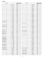
Page 36: ...nputs outputs are multiplexed on the same pins 3 VDDQ Data output power 4 5 DQ1 DQ2 Data inputs outputs are multiplexed on the same pins 6 VSSQ Data output ground 7 8 DQ3 DQ4 Data inputs outputs are multiplexed on the same pins 9 VDDQ Data output power 10 11 DQ5 DQ6 Data inputs outputs are multiplexed on the same pins 12 VSSQ Data inputs outputs are multiplexed on the same pins 13 DQ7 Dynamic powe...

Page 37: ...power 44 45 DQ9 DQ10 Data inputs outputs are multiplexed on the same pins 46 VSSQ Data output ground 47 48 DQ11 DQ12 Data inputs outputs are multiplexed on the same pins 48 DQ1 DQ2 Data inputs outputs are multiplexed on the same pins 49 VDDQ Data output power 50 51 DQ13 DQ14 Data inputs outputs are multiplexed on the same pins 52 VSSQ Data output ground 53 DQ15 Data inputs outputs are multiplexed ...

Page 38: ...HR MB3 8 9 MEMO ...

Page 39: ... set HR MB3 This document has been published to be used for after sales service only The contents are subject to change without notice 1 INTEGRATED CIRCUITS 2 TRANSISTORS 3 DIODES 4 COILS 5 VARIABLE CAPACITORS 6 VIBRATORS 7 CAPACITORS 8 RESISTORS 9 OTHER CIRCUITRY PARTS 10 CABINET PARTS 11 ACCESSORIES PACKING PARTS 12 P W B ASSEMBLY Not Replacement Item INDEX PORTABLE JUKEBOX MODEL HR MB3 S CONTEN...

Page 40: ...C Silicon KDS121E D402 VHDRB520S30 1 AC Schottky RB520S30 D403 VHDKDS121E 1 AC Silicon KDS121E D404 VHD1SS400 1 AB Silicon 1SS400 D405 VHDRB520S30 1 AC Schottky RB520S30 D406 VHD1SS400 1 AB Silicon 1SS400 D407 VHDFS1J3TP 1 AE Schottky FS1J3TP D408 VHEUDZS8R2B 1 AC Zener 8 2V UDZS8 2B D700 VHEUDZS33B 1 AC Zener 33V UDZS33B 4 COILS FB100 RCILCA015AWZZ AB Ferrite Beads FB101 RCILCA009AWZZ AB Coil FB1...

Page 41: ...lum C308 VCSATA0JJ106M AD 10 µ F 6 3V Electrolytic Tantalum C309 VCKYCZ1AB104K AB 0 1 µ F 10V C310 VCSATA0GJ107M 100 µ F 4V Electrolytic Tantalum C311 VCKYCZ1AB104K AB 0 1 µ F 10V C312 VCSATE0JJ107M AE 100 µ F 6 3V Electrolytic Tantalum C313 VCSATE0JJ107M AE 100 µ F 6 3V Electrolytic Tantalum C314 VCKYCZ1HB332K AA 0 0033 µ F 50V C315 VCKYCZ1HB332K AA 0 0033 µ F 50V C316 VCKYTV1AB105K AD 1 µ F 10V ...

Page 42: ...er 0 5x1 0mm R131 VRS CZ1JB473J AA 47 kohms 1 16W R132 VRS CZ1JB330J AA 33 ohms 1 16W R133 VRS CZ1JB330J AA 33 ohms 1 16W R134 VRS CZ1JB330J AA 33 ohms 1 16W R135 VRS CZ1JB330J AA 33 ohms 1 16W R136 VRS CZ1JB330J AA 33 ohms 1 16W R137 VRS TV2AB000J AA 0 ohm Jumper 1 25x2mm Green R140 VRS CZ1JB683J AB 68 kohms 1 16W R200 VRS CZ1JB154J AA 150 kohms 1 16W R201 VRS CZ1JB124J AB 120 kohms 1 16W R203 VR...

Page 43: ...mper 0 5x1 0mm R427 VRS CZ1JB154J AA 150 kohms 1 16W R428 VRS CZ1JB000J AB 0 ohm Jumper 0 5x1 0mm R429 VRS CZ1JB103J AA 10 kohm 1 16W R430 VRS CZ1JB103J AA 10 kohm 1 16W R433 VRS CZ1JB564J AA 560 kohms 1 16W R434 VRS CZ1JB562J AB 5 6 kohms 1 16W R435 VRS CZ1JB104J AA 100 kohm 1 16W R436 VRS CZ1JB332F AA 3 3 kohms 1 16W R437 VRS CZ1JB102J AB 1 kohm 1 16W R438 VRS CZ1JB000J AB 0 ohm Jumper 0 5x1 0mm...

Page 44: ...er On SW303 QSW K0237AFZZ AC Switch Key Type Function SW304 QSW K0237AFZZ AC Switch Key Type Skip Down Scroll Left Review SW305 QSW K0237AFZZ AC Switch Key Type Volume Up Scroll Up SW306 QSW K0237AFZZ AC Switch Key Type Volume Down Scroll Down SW307 QSW K0237AFZZ AC Switch Key Type Skip Up Scroll Right Cue SW401 QSW S0935AFZZ AD Switch Slide Type Battery ON OFF 10 CABINET PARTS 201 GCABAA042AWSA A...

Page 45: ...8AWZZ Unit Pad 8 SSAKHA056AWZZ Polyethylene Bag Set 9 TLABN0092AWZZ AB Label Serial No Packing Case For U K 9 TLABN0092AW02 AB Label Serial No Packing Case Except for U K 10 TLABZA314AWZZ Label Feature 11 TCADSA001AWZZ Card Service 1 TiNSEA114AWZZ Operation Manual 2 SPAKCA286AWZZ Packing Case 3 TiNSEA115AWZZ Quick Guide 4 RPHOHA005AWZZ Headphone 5 RADPAA007AWZZ AC Adapter 6 QCNWGA020AWZZ USB Cable...

Page 46: ... NO PARTS CODE PRICE RANK NEW MARK PART RANK DESCRIPTION 12 SPAKSA001AWZZ Sleeve 13 SPAKZ0490AWZZ AC Pad 14 Battery 12 P W B ASSEMBLY Not Replacement Item PWB A 92LPWB6362HDDS Main 11 ACCESSORIES PACKING PARTS ...

Page 47: ...013AWZZ 7 C101 AC 7 C102 AC 7 C103 AC 7 C125 AC 7 C126 AC 7 C129 AC 7 C500 AC 7 C510 AC 7 C703 AC RC KZ0014AWZZ 7 C402 AD 7 C403 AD 7 C404 AD 7 C405 AD 7 C406 AD 7 C413 AD 7 C414 AD 7 C417 AD 7 C418 AD 7 C422 AD RC KZ3017AWZZ 7 C427 AD 7 C429 AD RC KZ3021AWZZ 7 C426 AC RCRSCA007AWZZ 6 X100 AH RCRSCA009AWZZ 6 X200 AH RH IXA068AWZZ 1 IC100 BK RH IXA069AWZZ 1 IC500 BD RPHOHA005AWZZ 11 4 AU RUITDA004A...

Page 48: ...2 AH VHV10120MAB 1 5 VA301 AB 5 VA302 AB VPCEM100M0R7N 4 L100 AC VRS CZ1JB000J 8 R101 AB 8 R102 AB 8 R103 AB 8 R104 AB 8 R105 AB 8 R107 AB 8 R111 AB 8 R115 AB 8 R116 AB PARTS CODE No PRICE RANK NEW MARK PART RANK 8 R126 AB 8 R127 AB 8 R130 AB 8 R210 AB 8 R212 AB 8 R213 AB 8 R216 AB 8 R301 AB 8 R304 AB 8 R305 AB 8 R313 AB 8 R317 AB 8 R318 AB 8 R319 AB 8 R322 AB 8 R324 AB 8 R327 AB 8 R342 AB 8 R422 ...

Page 49: ...9 AA 8 R540 AA 8 R541 AA 8 R542 AA 8 R543 AA 8 R544 AA 8 R545 AA VRS CZ1JB332F 8 R436 AA VRS CZ1JB332J 8 R214 AB 8 R215 AB VRS CZ1JB333J 8 R405 AB VRS CZ1JB334F 8 R420 8 R425 VRS CZ1JB473J 8 R131 AA 8 R204 AA 8 R402 AA VRS CZ1JB474F 8 R419 AA VRS CZ1JB562J 8 R434 AB 8 R451 AB VRS CZ1JB564F 8 R410 AB VRS CZ1JB564J 8 R433 AA 8 R445 AA VRS CZ1JB681J 8 R443 AB 8 R452 AB 8 R453 AB VRS CZ1JB683J 8 R140 ...

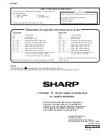
Page 50: ...llowing information 1 MODEL NUMBER 2 REF No 3 PART NO 4 DESCRIPTION MARK SPARE PARTS DELIVERY SECTION For U S A only Contact your nearest SHARP Parts Distributor to order For location of SHARP Parts Distributor Please call Toll Free 1 800 BE SHARP Explanation of capacitors resistors parts codes Capacitors VCC Ceramic type VCK Ceramic type VCT Semiconductor type VC MF Cylindrical type without lead ...

Reviews: