


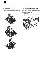

2. Description of main LSI’s
2-1. CPU (M30624FGFP)
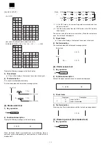
1) Pin configuration
2) Pin description
Pin
No.
SYMBOL
SIGNAL
NAME
In/Out
Function
1
SOUT4
P96
In
Key return :6
2
CLK4
P95
In
Key return :5
3
TB4IN
P94
In
Key return :4
4
TB3IN
P93
In
Key return :3
5
SOUT3
P92
In
Key return :2
6
SIN3
P91
In
Key return :1 and Master reset
SW
7
CLK3
P90
In
Key return :Mode SW
8
BYTE
VDD
In
VDD
9
CNVss
CNVss
In
Normal : L Booting : H
10
XCIN
XCIN
In
Calender clock :32.768KHz
11
XCOUT
XCOUT
In
Calender clock :32.768KHz
12
/RESET
/RESET
In
Reset
13
XOUT
XOUT
Out
System clock :12MHz
14
Vss
GND
In
GND
15
XIN
XIN
In
System clock :12MHz
16
Vcc
VDD
In
VDD
17
NMI
VDD
In
VDD
18
INT2
CTCRL
Out
Paper feed motor current control
19
INT1
/FRDY
In
FMC :Ready
20
INT0
P-OFF
In
Power off
21
TA4IN/U
MOTOR
Out
Paper take up motor drive
22
TA4OUT/U BUZ1
Out
Buzzer drive
23
TB3IN
P77
In
RS232 :DR
24
TBEOUT
P76
In
RS232 :CS
25
TA2INW
P75
In
RS232 :CD
26
TA2OUTW P74
Out
RS232 :ES
27
TA1IN/V
P73
Out
Printer head rank check On/Off
28
TA1OUT/V CLK
Out
Printer data clock
29
TB5IN
P71
Out
/HOLD control
30
TB5OUT
DAT
Out
Print data
31
TXD1
P67
Out
RS232 :SD
32
RXD1
P66
In
RS232 :RD
33
CLK1
/FRES
Out
FMC :Reset
34
CLKS1
P64
Out
RS232 :RS
35
TXD0
FSD
Out
FMC :Send data
36
RXD0
FRD
In
FMC :Receive data
37
CLK0
FSCK
Out
FMC :Shift clock
38
/RTS0
DR1
Out
Drawer drive
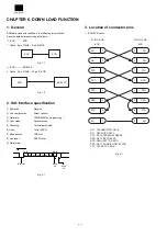
+24V : 24V
VLED : 5.7V
VDD : 5V
VCC : 5V
VH : 7.7V
Drawer
Display
Circuit
RAM
Printer
TRANSFORMER
LM2574HVM
MC34063
HI-MH
BATTERY
MC34063
F1
F2
F3
1
2
3
4
5
6
7
8
9
10
11
12
13
14
15
16
17
18
19
20
21
22
23
24
25
P96
P95
P94
P93
P92
P91
P90
VDD
GND
XCIN
XCOUT
/RESET
XOUT
GND
XIN
VDD
VDD
CTCRL
/FRDY
P-OFF
MOTOR
BUZ1
P77
P76
P75
TA2OUT
W
TA1IN/V
TA1OUT
/V
TB5IN
TB5OUT
TXD1
RXD1
CLK1
CLKS1
TXD0
RXD0
CLK0
/R
TS
0
/R
DY
ALE
/H
OL
D
/H
LDA
CBCLK
/R
D
/BHE
/WR
/C
S3
/C
S2
/C
S1
/C
S0
P74
P73
CLK
P71
DAT
P67
P66
/FRES
P64
FSD
FRD
FSCK
DR1
/R
DY
/H
OL
D
VCC
NC
NC
/R
D
NC
/WR
/C
S3
/R
AS
1
BUSY
/R
OS
1
SOUT4
CLK4
TB4IN
TB3IN
SOUT3
SIN3
CLK3
BYTE
CNVss
XCIN
XCOUT
/RESET
XOUT
Vss
XIN
Vcc
NMI
INT2
INT1
INT0
TA4IN/U
TA4OUT/U
TB3IN
TBEOUT
TA2INW
75
74
73
72
71
70
69
68
67
66
65
64
63
62
61
60
50
58
57
56
55
54
53
52
51
26
27
28
29
30
31
32
33
34
35
36
37
38
39
40
41
42
43
44
45
46
47
48
49
50
100
99
98
97
96
95
94
93
92
91
90
89
88
87
86
85
84
83
82
81
80
79
78
77
76
NC
NC
A17
A16
A15
A14
A13
A12
A11
A10
A9
VDD
A8
GND
A7
A6
A5
A4
A3
A2
A1
A0
PH4
PH3
PH2
A19
A18
A17
A16
A15
A14
A13
A12
A11
A10
A9
VCC
A8
VSS
A7
A6
A5
A4
A3
A2
A1
A0
D15
D14
D13
PH1
P13
P12
P11
P10
D7
D6
D5
D4
D3
D2
D1
D0
DTS
LATC
H
P105
P104
P103
Vref
P101
GND
TH
VDD
VDD
P97
D12
D11
D10
D9
D8
D7
D6
D5
D4
D3
D2
D1
D0
AN7
AN6
AN5
AN4
AN3
AN2
AN1
AV
SS
AN0
VREF
AVCC
SIN4
M30624FGFP


