


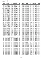
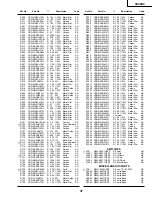

24
6
5
4
3
2
1
A
B
C
D
E
F
G
H
CX48K4
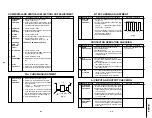
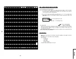
DESCRIPTION OF SCHEMATIC DIAGRAM
SAFETY NOTES:
1. DISCONNECT THE AC PLUG FROM THE AC OUTLET BEFORE
REPLACING PARTS.
2. SEMICONDUCTOR HEAT SINKS SHOULD BE REGARDED AS
POTENTIAL SHOCK HAZARDS WHEN THE CHASSIS IS OP-
ERATING.
IMPORTANT SAFETY NOTICE:
PARTS MARKED WITH “
å
” ( ) ARE IMPORTANT FOR
MAINTAINING THE SAFETY OF THE SET. BE SURE TO RE-
PLACE THESE PARTS WITH SPECIFIED ONES FOR MAINTAIN-
ING THE SAFETY AND PERFORMANCE OF THE SET.
SERVICE PRECAUTION:
THE AREA ENCLOSED BY THIS LINE ( ) IS DIRECTLY
CONNECTED WITH AC MAINS VOLTAGE.
WHEN SERVICING THE AREA, CONNECT AN ISOLATING TRANS-
FORMER BETWEEN TV RECEIVER AND AC LINE TO ELIMINATE
HAZARD OF ELECTRIC SHOCK.
NOTES:
1. The unit of resistance “ohm” is omitted.
(K = 1000 ohms, M = Meg ohm).
2. All resistors are 1/16 watt, unless otherwise noted.
3. All capacitors are
µ
F, unless therwise noted. (P =
µµ
F).
VOLTAGE MEASUREMENT CONDITIONS:
1. Voltage in parenthesis measured with no Signal.
2. Voltages without parenthesis measured with PAL Colour-Signal.
3. All the voltages in each point are measured with high impedence
volt-meter.
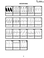
WAVEFORM MEASUREMENT CONDITIONS:
1. Colour bar generator signal of 1.8V peak to peak applied at Base
of Video Buffer Amp. Q200.
2. Approximately 4.0 V AGC bias.
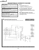
Ë
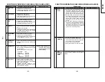
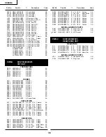
Infrared Remote Control Unit
NOTE : The parts here shown are supplied as an assembly but not independently.
RRMCG1342PESA
6
5
4
3
2
1
A
B
C
D
E
Summary of Contents for CX48K4
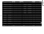
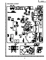
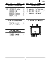
Page 19: ...19 6 5 4 3 2 1 A B C D E F G H CX48K4 CHASSIS LAYOUT ...
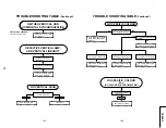
Page 20: ...21 CX48K4 20 BLOCK DIAGRAM 12 11 10 9 8 7 6 5 4 3 2 1 A B C D E F G H ...
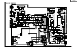
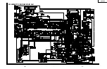
Page 21: ...22 6 5 4 3 2 1 A B C D E F G H CX48K4 ...
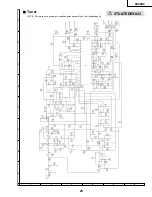
Page 25: ...27 CX48K4 26 SCHEMATIC DIAGRAM MAIN Unit 12 11 10 9 8 7 6 5 4 3 2 1 A B C D E F G H ...
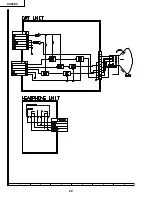
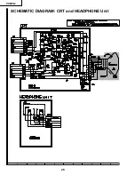
Page 26: ...28 6 5 4 3 2 1 A B C D E F G H CX48K4 SCHEMATIC DIAGRAM CRT and HEADPHONE Unit ...
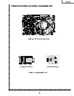
Page 28: ...31 CX48K4 30 PWB A MAIN Unit Component Side 12 11 10 9 8 7 6 5 4 3 2 1 A B C D E F G H ...
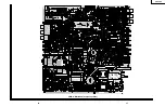
Page 29: ...33 CX48K4 32 PWB A MAIN Unit Chip Parts Side 12 11 10 9 8 7 6 5 4 3 2 1 A B C D E F G H ...


