background image

XL-T300H

– 44 –

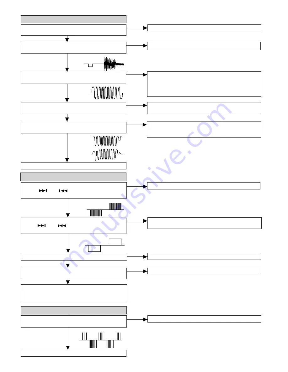
• Sled motor operation failure.

Yes

Yes

Is following sled feed signal output the pin 40 (FMO) of IC801
when FF 

 /REW 

 key is pressed after the CD TEST

MODE "STEP 1" is set?

Is sled feed signal output the pins 1 and 2 of IC803?

Is sled feed voltage applied between both terminals of sled
motor?

No

Check the peripheral parts of IC803. If OK, IC803 is faulty.

No

C801 is faulty.

Check the CNW802.

No

Yes

Check the CD mechanism (periphery of sled motor).
If the sled motor does not run when DC2.0V is applied to
both terminals of sled motor, the sled motor is faulty.

• Sled servo failure.

Yes

Is following sled signal output the pin 40 (FMO) of IC801
during playback?

Normal.

No

IC801 is faulty.

• Track search failure

Does the sled motor run in FF/REW state when the SERVO
TEST MODE "STEP1" is set?

Is the following wave output to the pin 34 (TRO) of IC801
during track search in normal playback?

Is the following wave output to the pins 11 (TEO) of IC802
during track search in normal playback?

Yes

Yes

No

Check as stated in item "SLED MOTOR OPERATION FAILURE".

No

IC801 failure.

No

Check the PWB pattern between pin 34 (TRO) of IC801 and pin
25 of IC803.
Check the PWB pattern between pins 26 and 27 of IC803 and
Optical pickup.
If OK.  Optical pickup failure.

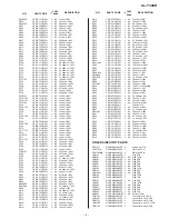
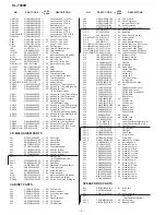
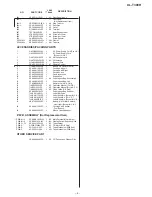
Yes

Is the above wave output to the pins 31 (TEI) and 32 (TEZI) of
IC801 during track search in normal playback?

No

Check the PWB pattern between pin 11 (TEO) of IC802 and pins 31
and 32 of IC801.  If OK. IC802 failure.

Normal.

Yes

Yes

Is following sled feed signal output the pins 3 and 4 of IC803
when FF 

 /REW 

 key is pressed after the CD TEST

MODE "STEP 1" is set?

Check the PWB pattern between pin 40 of IC801 and pins 3 and 4
of IC803.

No

Is the following wave output to the pin 27 (RFZI) and 28
(RFRP) of IC801 during track search in normal playback?

No

Check the PWB pattern between pins 22 (RFO),17 (RFRP), 19
(RFGO) and 20 (RFGC) of IC802 and pins 24,27,28 and 36 of IC801.
If OK. IC802 failure.

Yes

TRO

TEO

TEI

TEZI

FF

REW

FMO

FMO

RFZI

RFRP

FF

REW

SL 

±

Summary of Contents for CP-XLT300H

Page 1: ...D CIRCUIT 38 TROUBLESHOOTING 39 FUNCTION TABLE OF IC 45 LCD SEGMENT 47 PARTS GUIDE EXPLODED VIEW PACKING METHOD FOR U K ONLY SERVICE MANUAL SHARP CORPORATION No S4225XLT300H In the interests of user safety the set should be restored to its original condition and only parts identical to those specified should be used This document has been published to be used for after sales service only The conte...

Page 2: ...nit and replacementservicepartshavealreadybeenadjustedprior to shipping 3 No adjustment to the Laser Power should be attempted when replacing or servicing the Pickup 4 Under no circumstances look directly into the Pickup Lens at any time 5 CAUTION Use of controls or adjustments or performance of procedures other than those specified herein may result in hazardous radiation exposure SAFETY PRECAUTI...

Page 3: ... 6 ohms Headphones 16 50 ohms recommended 32 ohms CD digital output optical Input terminals Video Auxiliary audio signal 500 mV 47 kohms CD player Type Compact disc player Signal readout Non contact 3 beam semiconductor laser pickup D A converter 1 bit D A converter Frequency re sponse 20 20 000 Hz Dynamic range 90 dB 1 kHz Tuner Cassette deck Frequency range FM 87 5 108 MHz AM 522 1 620 kHz Frequ...

Page 4: ... Programme Indicator 8 Traffic Announcement Indicator 9 FM Stereo Mode Indicator 10 CD Play Indicator 11 CD Repeat Play Indicator 12 FM Stereo Receiving Indicator 13 Surround Indicator 1 3 4 5 6 7 8 9 11 13 10 12 2 1 2 3 4 5 6 7 8 9 10 11 12 Rear panel 1 Cooling Fan 2 Speaker Terminals 3 Headphone Socket 4 AM Aerial Terminal 5 Aerial Earth Terminal 6 FM 75 Ohms Aerial Socket 7 CD Digital Output So...

Page 5: ...n 19 CD Track Down Button 20 CD Fast Reverse Tuning Down Tape Rewind Button 21 CD or Tape Play Button 22 CD Track Up Button 23 CD Fast Forward Tuning Up Tape Fast Forward Button 24 CD Pause Button 25 CD or Tape Stop Button 26 Tuner Preset Down Button 27 Bass Up and Down Buttons 28 Treble Up and Down Buttons 29 RDS Programme Type Traffic Information Search Button 30 RDS ASPM Auto Station Programme ...

Page 6: ...lly to PM 4 Within 1 minute press the PRESET or button to adjust the minutes and then press the MEMORY button The clock starts from 0 second Seconds are not displayed 1 Clear all the programmed contents 2 Perform Setting the clock from the beginning Remote control Test of the remote control Face the remote control directly to the remote sensor on the unit The remote control can be used within the ...

Page 7: ...jected to strong external interference mechanical shock excessive static electricity abnormal supply voltage due to lightning etc or if it is operated incorrectly it may mal function If such a problem occurs do the following 1 Set the unit to the stand by mode and turn the power on again 2 If the unit is not restored in step 1 unplug and plug in the unit and then turn the power on 3 If neither ste...

Page 8: ...lectrostatic damage Caution on Disassembly Follow the below mentioned notes when disassembling the unit and reassembling it to keep it safe and ensure excellent performance 1 Take compact disc out of the unit 2 Be sure to remove the power supply plug from the wall outlet before starting to disassemble the unit 3 Take off nylon bands or wire holders where they need to be removed when disassembling ...

Page 9: ...m F1 x4 ø2 5 x10mm G1 x4 ø3 x10mm Holder PWB Hook L2 x4 Holder PWB Top Panel L1 x3 ø2 5 x10mm K1 x1 ø2 5 x10mm H2 x1 L1 x4 ø2 5 x8mm J1 x1 ø2 5 x8mm H1 x2 ø2 5 x10mm H1 x1 ø2 5 x10mm Switch PWB LED PWB Switch PWB Gear Box Display PWB A3 x2 ø3 x12mm A4 x4 ø4 x12mm A2 x2 Special screw Net Frame A1 x1 A2 x2 Special screw Woofer Tweeter Figure 9 2 1 Speaker 1 Net Frame A1 x1 9 4 2 Special Screw A2 x4 ...

Page 10: ... belt is not twisted and clean it How to remove the motor See Figs 10 4 1 Remove the mainbelt 2 Remove the screws D1 x 2 pcs to remove the motor bracket 3 Remove the screws D2 x 3 pcs to remove the motor Note Whenmountingthemotor payattentiontothemotormounting angle A Pinch Roller B1 x1 Pinch Roller Pawl REMOVING AND REINSTALLING THE MAIN PARTS Main Belt C1 x1 FF REW Belt C2 x1 REW FF Clutch Motor...

Page 11: ...eful so that the gear is not damaged The damage gear emits noise during searching A1 x2 ø2 x5mm Hook A2 x3 CD Lid Motor Figure 11 3 CD MECHANISM SECTION See Fig 11 3 Perform steps 1 and 6 of the disassembly method to remove the CD mechanism See page 8 9 1 Remove the mechanism cover paying attention to the pawls A1 x 4 pcs 2 Remove the screws A2 x 2 pcs to remove the shaft A3 x 1 pc 3 Remove the st...

Page 12: ...tion Display Frequency 87 5 MHz 87 5 MHz 2 2 V 0 7 V TP301 108 MHz 108 MHz 7 3 V 1 0 V TP301 Check FM VT Signal generator 1 kHz 40 kHz dev FM modulated 98 00 MHz 98 00 MHz VR351 1 Input SO301 30 dBµV Output Speaker Terminal Instrument Connection TUNER SECTION Setting the Test Mode Keeping the FF FWD button and MEMORY SET button pressed turn on ON STAND BY Then the frequency is initially set in the...

Page 13: ...nner periphery Any buttons other than ON STAND BY button are not accepted until the shift of pickup to the inner periphery is completed at this time If PICKUP IN SW ON cannot be detected within 10 seconds the slide motor stops and the following error display appears Press the ON STAND BY button to end the test mode or press the CD STOP button to return to step 1 Any other operations are inhibited ...

Page 14: ... toward the inner periphery while this button is pressed If PICKUP IN is on input is invalid PLAY If focus has been taken shift to step 4 is executed If not acceptance is inhibited STOP Return to step 1 FUNCTION Shift to step 5 If the focus is not received after it has been taken the process returns to step 1 3 Step 3 Mode While the laser keeps lighting CD initialization operation flow proceeds up...

Page 15: ...Press the following buttons in this state to obtain the operations specified below ON STAND BY Test mode and power turned off to shift to the ordinary standby mode FF FWD The pickup slides toward the outer periphery while this button is pressed REW REV The pickup slides toward the inner periphery while this button is pressed If PICKUP IN is on input is invalid PLAY Invalid STOP Return to step 1 FU...

Page 16: ...played in hexadecimal numbers The upper two bits which are invalid are displayed as 00 After waiting two seconds operation is shifted to c c Tb is displayed on the left of LCD FTBAST command D482 is transmitted to designate tracking balance adjusting register Then data read by read command SRC2 2 are displayed in hexadecimal numbers After waiting 2 seconds operation is shifted to d d TG is display...

Page 17: ...ching is invalid It is necessary to discard the content of preset memory when the tuner test mode is ended be sure to write 0000 or 1111 bits in the memory to be checked for judging memory error at initial setting and to initialize memory When the tuner test mode is obtained the following display lights for one second The TUNER TEST02 mode is obtained with MEMORY ON STAND BY Turn off AC in the TES...

Page 18: ...rding to the following procedure to reproduce the timer 1 Set the current time to 1 00 the timer to ON time 1 05 the function to CD and volume to STEP 12 respectively One minute is counted as one second and the timer is reproduced The fade in when playback is started is executed at a rate of one step for 1 sec After completion of fade in the fade out is executed at a rate of one step for 1 sec WAI...

Page 19: ... CD OPEN CLOSE The OK NG display of test result is as follows 7 Button input diagnosis Test Mode TEST 06 When the test mode is obtained the following is displayed a POWER ON for function AUX CD lid position is checked CLOSE position Operation proceeds to the next process Position other than CLOSE After the lid moves to CLOSE operation proceeds to the next process b CD lid operation started OPEN op...

Page 20: ... ohm type resistor Besides the one with Fusible is a fuse type Capacitor To indicate the unit of capacitor a symbol P is used this symbol P means micro micro farad and the unit of the capacitor without such a symbol is microfarad As to electrolyticcapacitor theexpression capacitance withstand voltage is used CH TH RH UJ Temperature compensation ML Mylar type P P Polypropylene type Schematic diagra...

Page 21: ...NT VDD 32 768kHz 8MHz 38 5 4 1 1 100 67 66 65 64 63 62 61 60 59 58 33 57 56 54 53 42 52 41 21 55 39 48 49 50 32 47 TAPE SW 22 8 4 LCD701 FL DISPLAY TO MAIN PWB REMOTE SENSOR RX701 RESET 23 VSM VLC1 VLC2 VLC3 7 6 5 MMOD VREF VREF VSS 15 24 14 11 SYS_STOP POWER 38 37 13 12 10 9 X701 X702 OSC1 OSC2 XO XI CLID_SW SW711 712 SW721 728 SW709 SW710 KEY1 KEY2 18 17 16 SYSTEM MICROCOMPUTER FL DRIVER IC701 I...

Page 22: ...US2 BUS3 BUCK CCE RST 53 50 RO LO 6 15 25 39 43 48 64 7 22 42 44 45 54 A_GND GND GND M_GND VOLTAGE REGULATOR ZD801 Q803 Q804A Q805 ZD802 LD MON FOCUS COIL 1 2V 5V TRACKING COIL CD PICKUP UNIT B6 SPINDLE MOTOR SLED MOTOR PICKUP IN SP SP SL SL PU IN GND M M CD MOTOR PWB M701 M702 SW702 SWITCHING Q171 Q172 B Q153 BEAT CANCEL B CAN REC BIAS REC BIAS CONT SWITCHING SWITCHING A 12V Q152 Q154 Q155 Q151 L...

Page 23: ...DD IC401 LC75342M 15 14 13 12 11 10 9 17 18 19 20 21 22 23 24 25 26 27 28 29 16 8 7 6 5 4 3 2 1 CE DI 30 CL LOGIC TUN L CD L TUN R R CH OUT R CH OUT L CH OUT R CH IN L CH IN L CH OUT A_12V NC FUNCTION VOLUME EQUALISER AUX R AUX L TAPE L CD R RMINAL PWB SWITCHING MUTE VOLTAGE REGULATOR B6 CH CH 1 O AUX T B5 A C B F E B5 AL D_GND MAIN PWB B4 B2 B Q461 Q463 B6 Q241 Q242 Q203 Q204 Q883 Q884 CD_L CD_R ...

Page 24: ...king AM ANT AM Band Coverage FM Mute Level AM IF AM IF 1 2 3 FM IF FM IF FM IF CH CH Low PassFil 0 022 1N4148 1N4148 0 022 560P 68K 27P 8P 0 047 0 022 SVC348S 0 001 0 012 0 001 1N4148 1N4148 4 7K 180 0 022 680 0 022 100 16 0 022 82 0 022 2 2µH 68 6 8K 330 2SC380 O 33 680 5 6K 5 6K 8 2K 1mH 10K 33P 3 3 50 0 022 0 022 4 7 25 0 022 0 001 2 7K 456kHz 1 50 0 022 LA1832S 270 0 022 0 022 1K 0 022 10 16 0...

Page 25: ... 1 2 3 CNP301 P28 5 A TO MAIN PWB A1 1 3 FM IF Low PassFilter 0 022 0 001 2 7K 456kHz 1 50 56P 1 50 1K 470K 0 027 0 027 6 8K 6 8K KRC104 M 5 6K 5 6K 1 50 1 50 2 2K 1 50 3 3K 2 2 50 0 001 100 10 0 047 270 0 022 0 022 0 022 2 2K 0 01 100µH 5 6K 1K 330P 47K 220P 1 50 10K DZ5 1BSB 100µH 100 10 0 022 390 0 022 390 5 6K KTA1266 GR 5 6K 5 6K 6 8K 47 16 1N4148 10K 4 7K 1 8K 0 022 56K 10K 56K KTC3199 GR 1N...

Page 26: ...IN PWB A1 1 3 1 1 3 2 3 2 1 2 3 CH CH SYSTEM MICROCOMPUTE FL DRIVER REMOTE SENSOR FL DISPLAY 1K 1K 1K 1K 1K 1K 1K 1K 1K 1K 1K 1K 1K 1K 1K 1K 1K 1K 1K 1K 1K 1K 1K 1K 1K 1K 12K 22P 22P 1K 0 1 10µH 10K 47K 1 2K 2 7K 2 7K 3 9K 2 2K 10K 1 2K 5 6K 47K 10µH 10K 10K 10K 220 LP3052D LP3052D 0 022 33K 47K 0 01 100 100 10 10 16 47K 0 022 47K 47K 47K 33K KRC102 M 2 2K 4 7K KTA1266 GR KRC102 M 10K 47K KTA1266 ...

Page 27: ... B LIGHT CLID_UP CLID_DW PU IN CD_RES CD_STB BUS1 BUS0 BUS2 BUS3 BUCK CCE 38 37 36 35 34 33 32 31 30 29 28 27 26 25 24 23 22 21 20 19 18 17 6 TAPE_SW U_CON5V SOL MOT REC RUN_PLS BIAS B_CAN CE DI CL DO STEREO SD VSM DATA CLE D_GND P_MUTE CD B SURROUND AMP_DET PROTECT FAN_DET M_12V B B B B B B B B B B B B B B FAN_CONT M_GND SP_RLY CD_STB CD_RES CCE BUCK BUS3 BUS2 BUS1 BUS0 PU IN CD_RW CLID_SW CLID_P...

Page 28: ... CNW705 P27 12 E FROM DISPLAY PWB B1 1 3 2 3 1 2 CONSTANT VOLTAGE REGULATOR RELAY LINE FILTER CNS301 P25 11 D E FROM TUNER PWB C 2 7K 2 7K 27K 27K 1N4148 1N4148 0 0047 0 82µH 0 0022 100 10 2 2µH 1K 1K 820 DZ130BSA 0 022 KTC3200 GR 100 100 25 1N4148 22K 470 25 47 2SD2012 Y 22K 2SD2012 Y 47 0 022 10 16 KRC107 M 820 KRA102 M 0 022 22K KTC3200 GR 2SD2012 Y 47 1N4148 10 16 470 25 100 100 25 33K DZ8 2BS...

Page 29: ...0 0 0027 1 50 0 1 0 1 3 9K 1K 10 16 0 0022 6 8 0 022 0 022 0 022 0 022 0 022 0 0022 6 8 0 022 1N4004 KTC3199 GR 47K 0 022 0 022 6 8 0 022 0 022 6 8 KTC3199 GR 4 7K 0 022 4 7K 1N4148 0 2 KTC3199 GR 1N4148 4 7K 0 022 0 2 4 7K 10 50 39K 3P 10 50 1K 0 0015 100 100 50 56K 1K 470 10 50 10 50 33 16 6 8K 10K 10K KTC3199 GR KTC3199 GR 3 3K 1K 470 22K 0 0015 10 50 1K 100 50 56K 3P 1K 39K 100 10 50 10µH 820P...

Page 30: ...8 C B TR TR PO FO GND A E LD VR PD C VIN1 VG1 TRB REG MUTE GND GND GND VG2 VIN2 V02 V02 V03 OPO PO1 PO1 VO3 VIN3 VG3 VCC VCC BIAS VG4 VIN4 V04 V04 VO1 VO1 2 5 7 3 15 13 1 8 9 6 10 11 4 14 12 16 2 5 7 3 15 13 1 8 9 6 10 11 4 14 12 16 SP SP SL SL PU IN GND 5 1 4 3 2 6 4 5 2 6 1 4 3 CD MOTOR PWB D GND PU IN SL SP SP SP PICKUP IN SLED MOTOR SPINDLE MOTOR M 4 6 M 2 M 3 5 1 MAIN PWB A1 2 3 C3A C2A C4A V...

Page 31: ...C FROM TERMINAL PWB A2 P29 8 H TO MAIN PWB A1 1 3 P28 1 F TO MAIN PWB A1 1 3 CD SIGNAL 1 1 2 2 3 3 CH CH 100mA CH CH CH 33K 7K 10K 100 10K 22P 8 2K 0 1 0 1 100 10 100 10 47 10 0 1 47P 47K 0 015 15K 150K 5 6K 0 0027 0 01 10K 0 033 0 047 470P 470P 0 033 4 7K 0 047 0 047 TC94A14F 10 10 100 10 10 10 15P 1M 12P 100 10 0 022 0 047 0 047 47 10 0 1 0 0068 2 2µH 2 2µH 0 022 100 10 0 022 DZ5 1BSB 100 390K 1...

Page 32: ...D SIGNAL 1 2 1 2 3 1 2 3 1 2 3 PHOTO INTERRUPTER TAPE MECHANISM PWB F HEAD SELECTOR 18K 1N4148 270 47K 3 3 50 KRC107 M 33K 0 001 10K 0 001 82P 1K 820P 2 7K 0 001 1K 82P 330 BA3126N 4 7 25 KTC3199 GR 4 7K 4 7K 4 7K KTC3199 G 4 7K KTC3199 GR 5 6K 4 7 25 10 16 100K KRA102 M KRC102 M 47K 100K 0 0039 2SC2001 K KTA12 10K 10 100 16 KRC104 330µH 0 027 180P 0 001 5 6K 5 6K 0 022 KTC3199 GR KTC3199 GR KTC31...

Page 33: ...0 001 2SB562 C 10K KRC102 M C3199 GR 15K 4 7K 4 7K 100 0 0012 33K 4 7 25 4 7 25 33K 0 0012 100 4 7K KTC3199 GR 4 7K TC3199 GR 10 16 100K 15K 330P 330P 270P 120 47 16 150K 0 015 3 9K 10 16 4 7K KTC3199 GR 820 10K 100 25 330 22 16 100K 1K 0 022 2 2 50 BA3311L 10 16 47 16 120 10K 0 015 3 9K 150K 1N4148 KTC3199 GR 820 4 7K 10K 100K C2001 K KTA1266 GR 10K 10K 56 100 16 150 150 KRC104 M 330µH 7 270P KRC...

Page 34: ... WH W BK PK BROWN RED ORANGE YELLOW GREEN BLUE VIOLET GRAY WHITE BLACK PINK CD LID MOTOR CD LID GY RD GY GY GY GY GY GY GY GY BK GY RD GY BK BK BK BK BK 1 2 MOTOR PWB A3 SWITCH PWB B2 SWITCH PWB B3 LED PWB B5 13 12 2 1 1 2 3 4 5 6 7 BK GY GY GY GY GY GY 7 6 5 4 3 2 1 TAPE MECHANISM ASS Y 212 TAPE MECHANISM PWB E F RECORD PLAYBACK HEAD ERASE HEAD WH BK GR 1 2 3 4 5 6 7 8 9 GR RD WH BK P37 8 F TO MA...

Page 35: ...1 1 2 3 4 5 6 7 8 9 10 11 12 13 14 15 16 17 18 19 20 21 22 23 24 25 26 27 28 29 30 31 32 33 34 35 36 37 38 5 10 15 20 25 26 30 35 40 45 50 51 55 60 65 70 75 76 80 85 90 95 100 1 1 1 7 6 B B C E E C B 1 2 3 3 2 1 B C E B C E 1 2 3 C E 1 2 3 13 1 10 1 1 3 8 1 2 CD PICKUP UNIT 308 1 3 5 7 9 11 13 15 2 4 6 8 10 12 14 16 CD MOTOR PWB D SPINDLE MOTOR BK BK WH WH BK BK BK BK BK GY GY GY GY GY GY GY GY GY...

Page 36: ...1 D807 D808 C109 C125 C123 C401 CNP IC102 C111 C Q10 R C117 D104 C108 C126 C129 C112 R112 R111 Q106 Q105 C110 R461 R201 R468 C463 R462 R478 R477 C469 C415 C474 C425 C476 C473 C475 C464 C478 C417 R472 IC201 C407 R467 Q461 CNW401 Q463 D461 CNW804 J801 SO401 R529 R528 CNS301 Q521 X521 C521 L521 Q351 C535 R521 D521 ZD351 C537 C396 C358 C357 R377 C391 R395 R391 R392 R385 R384 L352 C370 C398 CF351 C399 ...

Page 37: ...0 ZD801 R826 Q804 D803 R855 C803 D804 R864 C872 C808 CNW802 C857 L802 Q802 C846 L805 R835 R811 R809 C805 R815 C839 D801 Q801 C822 L801 R801 R856 R804 R819 R803 CNW909 R821 C812 C807 C819 R837 D802 C850 C851 C825 CNP804 C853 CNP704 C854 X801 C856 C869 Q803 C868 ZD802 Q805 D902 C903 Q905 R906 R907 D904 R902 D903 R901 Q901 Q902 Q904 Q906 C902 Q903 D901 CNW901 Q172 CNP101 C130 Q104 Q171 R138 Q102 Q101...

Page 38: ...C801 40pin STOP PLAY CUE FEI 1 TEI 1 IC801 29pin SBAD 2 TRO 2 IC801 30pin IC801 34pin RFO 3 FMO 3 IC802 22pin IC801 40pin STOP PLAY REVIEW FEI 1 TEI 1 IC801 29pin RFGO 2 TRO 2 IC802 19pin IC801 34pin RFRP 3 FMO 3 IC802 17pin IC801 40pin STOP PLAY TCD 782 TNO 02 PLAYBACK TEI 1 LO 1 IC801 31pin TRO 2 IC801 34pin RO 2 SBAD 3 IC801 30pin 1 2 3 4 6 7 11 15 16 17 IC801 53pin IC801 31pin IC801 31pin IC80...

Page 39: ...be used on car CD player or on computer CD ROM drives All rights reserved Unauthorized duplicating broadcasting and renting product is prohibited by law When the CD does not function When the CD section does not operate when the objective lens of the optical pickup is dirty this section may not operate Clean the objective lens and check the playback operation When this section does not operate eve...

Page 40: ...e HF output on pin 24 of IC801 in CD TEST MODE STEP 5 Check the procedure HF ERROR Yes No No No No Check the pattern between pin 58 PU_IN of IC701 and CNW704 CNP704 Check the between CNW704 CNP704 and PU IN switch Set ON condition the CD Lid switch Check the procedure in SPINDLE MOTOR CLV SERVO FAILURE No Does the sled motor move No Does the sound heard when the optical pickup move to the selected...

Page 41: ...e pin 29 FEI of IC801 when the disc is set Is the waveform shown above input at the pin 30 SBAD of IC801 Yes Yes No No The optical pickup is faulty Check as stated in item FOCUS SERVO SAWTOOTH WAVE FAILURE Yes Check the periphery of IC802 and CNP801 CNW801 Is it normal No Check the pattern between pin 12 of IC802 and pin 30 of IC801 Check the periphery of IC802 and CNP801 CNW801 IC802 is faulty Ye...

Page 42: ...etween pins 13 and 16 of CNP801 CNW801 as shown above Yes Check the PWB pattern between CNP801 CNW801 and IC803 No CNP801 CNW801 connection failure or optical pickup failure Yes Spindle motor clv servo failure Is above wave obtained between pins 1 and 2 of IC803 Is following wave output to the pin 41 DMO of IC801 when the CD TEST MODE STEP 3 is changed to STEP 4 No Yes Check the procedure in HF ER...

Page 43: ...50 or 53 of IC801 and the pins 1 or 15 of IC601 No Check the PWB pattern between pin 51 of IC801 and Q803 Yes Is signal of pins 50 and 53 of IC801 output No Check the peripheral parts of IC801 If OK IC801 is faulty Yes The main PWB is faulty Check the periphery of IC802 Check the PWB pattern between pin 11 TEO of IC802 and pins 31 and 32 of IC801 Is it normal Is output obtained at the pins 3 and 8...

Page 44: ...the following wave output to the pins 11 TEO of IC802 during track search in normal playback Yes Yes No Check as stated in item SLED MOTOR OPERATION FAILURE No IC801 failure No Check the PWB pattern between pin 34 TRO of IC801 and pin 25 of IC803 Check the PWB pattern between pins 26 and 27 of IC803 and Optical pickup If OK Optical pickup failure Yes Is the above wave output to the pins 31 TEI and...

Page 45: ...L1 Input signal pin 15 NC No CONNECT pin To be open or connected to VSS 16 NC No CONNECT pin To be open or connected to VSS 17 R1 Input signal pin 18 R2 Input signal pin 19 R3 Input signal pin 20 R4 Input signal pin 21 RSEL0 Input selector output pin 22 RIN Volume equalizer input pin 23 RTRE Capacitor connection pin comprising treble band filter 24 RBASS1 Bass band filter comprising capacitor and ...

Page 46: ...4 15 16 17 18 19 20 21 22 23 24 25 26 5 27 28 30 29 1 2 3 4 LVref RVref CCB INTERFACE CONTROL CIRCUIT LOGIC CIRCUIT CONTROL CIRCUIT ROUT RBASS1 RBASS2 RTRE RIN RSEL0 L1 L2 L3 L4 R1 R2 R3 R4 LOUT LBASS2 LBASS1 LTRE LIN LSEL0 VSS CE DI CL VDD NC Vref NC NC TEST Figure 46 BLOCK DIAGRAM OF IC ...

Page 47: ...l4 m4 f4 c5 com4 com4 z2 k1 d1 e1 z3 k2 d2 e2 MHz k3 d3 e3 kHz k4 d4 e4 z4 PinNo 22 23 24 25 26 27 28 29 30 31 32 33 34 35 36 37 38 39 40 41 42 com1 h5 g5 a5 RDS h6 g6 a6 r h7 g7 a7 TP h8 g8 a8 EON com1 com2 j5 n5 p5 b6 j6 n6 p6 b7 j7 n7 p7 b8 j8 n8 p8 PTY com2 com3 l5 m5 f5 c6 l6 m6 f6 c7 l7 m7 f7 c8 l8 m8 f8 TI com3 com4 k5 d5 e5 ST k6 d6 e6 q k7 d7 e7 k8 d8 e8 TA SRS 0 com4 z1 z2 z3 r q z4 1 2 ...

Page 48: ...XL T300H 48 MEMO ...

Page 49: ...indrical type without lead wire VC TV Square type without lead wire VC TQ Square type without lead wire VC CY Square type without lead wire VC CZ Square type without lead wire VC J The 13th character represents capacity difference J 5 K 10 M 20 N 30 C 0 25 pF D 0 5 pF Z 80 20 If there are no indications for the electrolytic capacitors error is 20 Resistors VRD Carbon film type VRS Carbon film type...

Page 50: ...03 VSKRC107M 1 J AC Digital NPN KRC107 M Q904 VSKRC102M 1 J AC Digital NPN KRC102 M Q905 VS2SB562 C 1 J AD Silicon PNP 2SB562 C Q906 VSKRA102M 1 J AC Digital PNP KRA102 M DIODES D104 VHD1N4148 1 J AA Silicon 1N4148 D201 203 VHD1N4148 1 J AA Silicon 1N4148 D204 VHD1N4004 1 J AB Silicon 1N4004 D301 304 VHD1N4148 1 J AA Silicon 1N4148 D308 VHD1N4148 1 J AA Silicon 1N4148 D401 403 VHD1N4004 1 J AB Sil...

Page 51: ... RC GZA107AF1A J AB 100 µF 10V Electrolytic C399 VCKYPA1HF473Z J AB 0 047 µF 50V C401 402 RC GZA106AF1C J AB 10 µF 16V Electrolytic C403 RC EZD106AF1C J AB 10 µF 16V Electrolytic C404 408 RC GZA106AF1C J AB 10 µF 16V Electrolytic C413 VCKYPA1HB472K J AB 0 0047 µF 50V C415 RC EZD106AF1C J AB 10 µF 16V Electrolytic C416 RC GZA106AF1C J AB 10 µF 16V Electrolytic C417 RC EZD225AF1H J AB 2 2 µF 50V Ele...

Page 52: ... 4W R156 157 VRD ST2EE151J J AA 150 ohms 1 4W R159 160 VRS CY1JB562J J AA 5 6 kohms 1 16W R201 202 VRD ST2CD102J J AA 1 kohm 1 6W R203 204 VRD ST2EE103J J AA 10 kohm 1 4W R205 VRD ST2EE332J J AA 3 3 kohms 1 4W R206 VRD ST2EE682J J AA 6 8 kohms 1 4W R207 208 VRD ST2CD393J J AA 39 kohms 1 6W R209 210 VRD ST2EE102J J AA 1 kohm 1 4W R211 212 VRD ST2EE471J J AA 470 ohms 1 4W R213 214 VRD ST2CD102J J AA...

Page 53: ...A 47 kohms 1 16W R813 VRD ST2CD152J J AA 1 5 kohms 1 6W R815 VRD ST2CD821J J AA 820 ohms 1 6W R816 VRS CY1JB101J J AA 100 ohm 1 16W R817 VRS CY1JB473J J AA 47 kohms 1 16W R818 VRS CY1JB103J J AA 10 kohm 1 16W R819 VRD ST2CD333J J AA 33 kohms 1 6W R820 VRS CY1JB103J J AA 10 kohm 1 16W R821 VRD ST2CD822J J AA 8 2 kohms 1 6W R824 VRS CY1JB473J J AA 47 kohms 1 16W R825 VRS CY1JB222J J AA 2 2 kohms 1 1...

Page 54: ... CABINET PARTS 201 GCABA1079SJSA J AQ Top Cabinet 202 GCABB1080SJSA J AN Bottom Cabinet 203 GCOVA1018SJSA J AD Cover Remote Sensor 204 GFTAT1014SJSA J AN CD Lid 205 HDECA1018SJSA J AS Plate Operation 206 HDECQ0079SJSA J AN CD Window 207 HDECQ0080SJSA J AF CD Illuminator 208 HDECQ0081SJSA J AE LCD Window 209 HDECQ0082SJSA J AF Plate Decoration 210 HDECQ0083SJSA J Indicator Panel LCD 211 JKNBZ0063SJ...

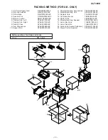
Page 55: ...Z J Pad Accessories 10 SPAKZ0067SJZZ J Support Pad 11 SSAKA0009SJZZ J AE Polyethylene Bag Accessories 12 SSAKH0018SJZZ J Polyethylene Bag Unit 13 TCADN0003SJZZ J Register Card U K Only 14 TINSE0082SJZZ J AF Operation Manual For U K 14 TINSZ0126SJZZ J AP Operation Manual Except for U K 15 TINSE0083SJZZ J AD Quick Guide U K Only 16 SPAKZ0061SJZZ J Polyethylene Bag Speaker 17 TLABE0108SJ01 J Label Ba...

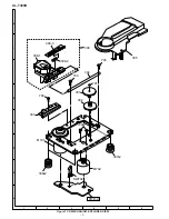
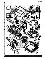
Page 56: ...XL T300H A B C D E F G H 1 2 3 4 5 6 Figure 7 CD MECHANISM EXPLODED VIEW 7 308 1 703 304 703 303 302 704 301 M701 702x2 306x2 SW702 M702 PWB D 308 3 308 2 308 701 305 307x2 ...

Page 57: ...36 231 620 616 616x2 616x2 610 610x2 614 603 616 608x9 619 616x5 607x3 608x3 608 606x4 605x4 606x3 609 606 606x2 605 606 226 225 216 219 242 202 218 215 209 206 204 207 205 208 233x3 235 217 243 201 203 220 224 223x2 211 212 212 1 212 2 212 5 212 6 212 3 212 4 212 7 212 8 212 9 212 10 212 11 241 243 1 243 4 243 3 243 2 243 5 243 6 M801 611x2 PWB A3 PWB A4 PWB A1 PWB A2 PWB C1 PWB B5 PWB B3 PWB B2 ...

Page 58: ... SP604 R CH SP601 L CH SP602 R CH SP603 L CH SP604 R CH Tweeter Tweeter Capacitor Capacitor 2 2µF 50V SP601 L CH SP602 R CH Woofer Woofer Red Red Black Black 907 901 906 902x2 905 909x4 SP601 SP602 SP603 SP604 908x2 903 3 903 2x2 903 2x2 904 1 904 903 904 3 904 2 910x2 910x2 903 1 ...

Page 59: ...KZ0066SJZZ 10 Support Pad SPAKZ0067SJZZ 11 Polyethylene Bag Accessories SSAKA0009SJZZ 12 Polyethylene Bag Unit SSAKH0018SJZZ 13 Register Card TCADN0003SJZZ 14 Operation Manual TINSE0082SJZZ 15 Quick Guide TINSE0083SJZZ 16 Polyethylene Bag Speaker SPAKZ0061SJZZ 17 Label Bar Code TLABE0108SJZZ 19 Label Serial No TLABN0180SJZZ 22 Packing Add Speaker Top Bottom SPAKA0110SJZZ 23 Sleeve Carton Speaker S...

Page 60: ...ma 739 0192 Japan Printed in Japan COPYRIGHT 2002 BY SHARP CORPORATION ALL RIGHTS RESERVED No part of this publication may be reproduced stored in a retrieval system or transmitted in any from or by any means electronic mechanical photocopying recording or otherwise without prior written permission of the publisher ...

Reviews: