background image

CD-C621H

– 40 –

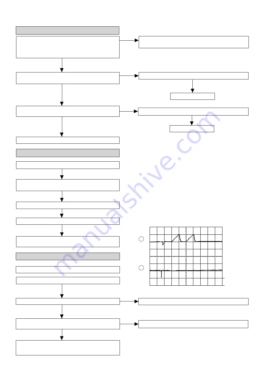
•  When the CD tray fails to open or close.

Is there following voltage input in specific state of IC701 pin 19?

     Open state: 0V

     Close state: 0V
  Intermediate state between open state and close state: 4.3V

Is H output to IC2 pin 24 or 25 for 7 seconds when the OPEN/
CLOSE key is pressed?IC91 is defective. Replace it.

Is 4V output between IC91 pins 3 and 7 during operation
stated above?

Check the loading motor (M1) and the loading mechanism.

Yes

Yes

Yes

No

No

IC2 defective.

No

Check the periphery of IC91.

IC91 defective.

OK

OK

Check the OPEN CLOSE SW and the wiring from the IC701
pin 19 to the OPEN CLOSE SW.

Check the wiring of the IC2 pins 24 and 25, IC91 pins 1 and 3.

•  The CD function will not work.

The CD operating keys don't work.

Check the CD, DSP, power supply, and 16.93 MHz clock, and
reset terminal.

Check the waveform of SCK, SO (DATA) and SI (COMM).

Yes

Yes

See if the pick-up is in the pick-up in PICKUP IN SW position.

If the items mentioned above are OK, check the main
microcomputer IC701.

Yes

Yes

No

Yes

No

•  The CD operating keys work.

Check the Focus - HF system.

Playback can be performed without a disc.

Focus search OK

Does the pick-up move up and down twice?

Does the output waveform of IC1(16)(FD) match that shown in
Fig. 40?

Check the IC1(50)(CLK) line, 4MHz.
Check the microcomputer data on pins (51)(CL), (52)(DAT)
and (53)CE.

Check the area around IC5-CNP2.

Yes

Yes

Figure 40

Focus search is
performed two
times when play
operation is done
without disc.

 0.5s
0.50 V
IC1  16  FD

2

1

 0.5s
0.50 V
IC1   7  TE

Summary of Contents for CD-C621H

Page 1: ...bs each CP C621H GBOXS0025AWM1 General Power source AC 230 V 50 Hz Power consumption Stand by 0 6 W Power on 89 W Dimensions Width 270 mm 10 5 8 Height 300 mm 11 13 16 Depth 351 mm 13 13 16 Weight 6 2 kg 13 7 lbs Amplifier section Output power PMPO 576 W Except for UK MPO 144 W 72 W 72 W DIN 45 324 RMS 80 W 40 W 40 W DIN 45 324 RMS 66 W 33 W 33 W DIN 45 500 Output power RMS 80 W 40 W 40 W For UK 1...

Page 2: ...e a cleaning disc designed for CD optical pickup lenses HOW TO USE 1 Using the brush in the cleaner cap apply 1 or 2 drops of the cleaning fluid to the brush on the CD cleaner disc which has the mark next to it 2 Place the CD cleaner disc onto the CD disc tray with the brush side down then press the play button 3 You will hear musicfor about 20 seconds and the CD player will automatically stop If ...

Page 3: ...ecific state When the CD mechanism is moved up 0V In other states 4 3V Yes Is there following voltage input on the IC701 pin 21 in the specific state In other states 4 3V When the CD mechanism is moved up 0V When turntable fails to move Check the MECHA UP SW and the wiring from the IC701 pin 21 to the MECHA UP SW Is 4V output from the Q91 emitter during operation stated above Yes Yes Check the wir...

Page 4: ... and 25 IC91 pins 1 and 3 The CD function will not work The CD operating keys don t work Check the CD DSP power supply and 16 93 MHz clock and reset terminal Check the waveform of SCK SO DATA and SI COMM Yes Yes See if the pick up is in the pick up in PICKUP IN SW position If the items mentioned above are OK check the main microcomputer IC701 Yes Yes No Yes No The CD operating keys work Check the ...

Page 5: ...gure 41 2 Figure 41 1 Waveform in case of normal play back HF 1 0V DIV 0 5µsec DIV DC When playing back the disc 3 2 1 4 0 5s 1 00 V IC1 16 FD 0 5s 10 0 V IC2 13 CLV 0 5s 10 0 V IC1 54 DRF 0 5s 2 00 V IC1 7 TE Check the tracking system Check waveform of IC1 pin 7 TE Play is possible in TEST mode Although IL is possible play is impossible Check the periphery of IC 1 pin 14 Normal jump is impeded an...

Page 6: ...performed when disc exits Yes Although HF waveform is normal TOC data cannot be read Yes Check PDO waveform Fig 42 Abnormal Check the IC1 pins 43 and 44 IC2 pins 3 5 7 10 and 11 Stop Play As VCO freque ncy is locked at 4 32 M Hz voltage of PDO rises and stabili zes 2 3 0 5s 1 00 V IC2 3 PDO 0 5s 1 00 V IC2 16 FD Although HF waveform is normal and the time indication is normal no sound is emitted C...

Page 7: ...0 1 1V 1 1V 2 2V 2 2V 1 1V 1 1V 2V 2V 0 2V 0 1V 2 0V 0 8V 0V 1 8V 0 4V 0 8V 17 16 15 14 13 20 19 18 2 6V 2V 2 6V 2V 5 1V 5 1V 3 6V 3 6V 21 24 23 22 PIN NO VOLTAGE IC303 0 2V 11 8V 4 1V 4 1V 2 6V 2 6V 0V 0V 0V 0 5V 0V 0V 4 7V 4 7V 0 5V 0 1V 0 2V 0 2V 0V 0V 5 1V 5 1V 2 5V 2 5V 9 8 7 6 5 4 3 2 1 12 11 10 0V 2 5V 5 1V 5 1V 0V 0V 2 5V 0V 5 1V 5 1V 0 9V 0 9V 0 9V 0 9V 1 9V 1 1V 17 16 15 14 13 20 19 18 0...

Page 8: ... 5ms 5 0 V HFL 0 5ms 5 0 V TES REVIEW 50ms 10 0 V JP CUE 50ms 10 0 V JP 50ms 0 50 V JP 50ms 1 00 V TE 0 5ms 10 0 V JP 0 5ms 10 0 V JP 0 5ms 0 50 V JP 0 5ms 1 00 V TE REVIEW 50ms 10 0 V JP 50ms 10 0 V JP 50ms 0 50 V JP 50ms 1 00 V TE 0 5ms 10 0 V JP 0 5ms 10 0 V JP 0 5ms 0 50 V JP 0 5ms 1 00 V TE PLAY 20ms 1 00 V SPO NORMAL DISC TN0 01 20ms 2 00 V CLV PLAY TCD 712 140mm TN0 01 50ms 1 00 V SPO 50ms ...

Page 9: ...R629 560 1 2W R635 330 R636 330 C629 22 25 R628 22K R617 2 2K R618 2 2K R614 10K C623 0 001 C624 0 001 Q602 2SC3331 Q601 2SC3331 C634 0 0047 C635 0 0047 R646 100K R645 100K C626 0 001 C625 0 001 Q604 2SC3331 Q603 2SC3331 C115 47 25 C116 47 25 R135 8 2K C129 470P C127 0 022 C128 3 3 50 C131 R137 6 8K C121 1 50 R123 3 9K C119 560P C117 0 033 C130 C132 R138 6 8K R132 33K R120 56 C120 560P R126 5 6K R...

Page 10: ...127 0 022 C128 3 3 50 C131 0 001 C146 220 10 R146 10K C135 0 068 C139 0 0033 R145 10K R137 6 8K C121 1 50 3 9K 9 P C145 22 25 C140 0 0033 C130 470P C142 1 50 R140 560 C132 0 001 R138 6 8K C134 22 25 R132 33K 20 P R126 5 6K C136 0 068 R142 56 3 9K C122 1 50 R125 5 6K R131 33K C133 22 25 9 8 7 6 5 4 Q122 2SC3331 C156 3 3 50 C154 47 16 R156 220K R174 5 6K 70 0 R175 1K 2SC3331 C630 0 022 D601 1SS133 D...

Page 11: ... C923 120P D803 1N4004S D806 1N4004S D805 1N4004S D804 1N4004S ZD80 MTZJ C804 47 50 Q801 KTA1274 R806 2 2K 1 2 3 4 5 6 7 8 9 10 11 12 13 14 15 Q905 2SC3331 R931 10K R929 1K C921 0 022 R938 56K R939 56K C920 0 022 R926 0 1 1W R803 47K C802 100 35 ZD801 MTZJ6 2A C803 47 50 R802 10 2 C830 47 25 C821 0 047 ML R837 10K C832 0 1 ML C831 47 25 2 C911 100 50 C912 100 50 R913 100 1 4W Fusible R966 22K C905...

Page 12: ... 50 RL801 C961 47 50 CNP804 R960 150 R967 150 14 15 D907 1SS133 R938 56K R939 56K R949 330 1 2W R941 4 7K R942 4 7K R952 68 C962 270P D961 1SS133 D962 1SS133 R951 68 Q960 2SC3331 1 2 3 4 5 6 7 8 R803 47K C802 100 35 ZD801 MTZJ6 2A C803 47 50 R802 10 1 2 CNP801 T802 C801 0 0047 M M901 FAN MOTOR 1 2 T801 POWER TRANSFORMER C810 470 35 Q803 AN78L05 1 D816 1SS133 2 3 C814 10 16 R808 220 C815 1000 6 3 D...

Page 13: ...CNP701 TO MAIN PWB C702 1 50 BI701 4 1 8 7 2 3 5 6 4 1 8 2 3 5 6 7 NC DISTOUT SPN_P SP_DET SPRLY DIST0 DIST0 L DEMOSTART DIST0 H ECOSTART REC PLAY AC RLY CON 5V 15V SPA SIG A_GND TUN_SM 12V M D_GND REC PLAY T_BIAS T_T1 T2 S MUTE HI_CUT SP_RLY SP_DET SPN_P VLOAD VP VF2 VF1 DO CLK CE DI 12V 12V 12V 12V 0V 0V U D SW VDD G5 G6 G7 G8 G9 P1 P10 P11 P2 P3 P4 P5 P6 P7 P8 VLOAD P16 HI CUT S MUTE T_T1T2 T B...

Page 14: ...2 3 4 5 6 7 8 9 RS706 470 RS707 470 SW708 SW709 SW707 SW706 SW705 FW702 SW704 SW703 SW701 0 L DEMOSTART 0 H ECOSTART AY CON 5V BACK UP CD PTY TI SEARCH TAPE VIDEO MEMORY SET REC PAUSE U D SW VDD G1 G2 G3 G4 G5 G6 G7 G8 G9 P1 P10 P11 DNO SW VSS REMOCON SYS STOP O C SW PUIN SW T2 RUN SPEANA1 SPEANA2 SPEANA3 AVSS SLD SLD FRF DRF SQOUT PCCL VPP LCK1 CLK DO CD DSP RES CD DSP WRQ CD DSP RWC CD DSP COIN ...

Page 15: ...2 31 30 29 28 27 26 25 24 23 22 19 20 21 42 41 40 39 38 37 C76 0 022 CNP12 CNP2 CNS12 P25 12 B TO DISPLAY PWB CNP3 6 5 4 3 2 1 2 3 4 5 1 CNS1A CNS1B 2 3 4 5 1 CNS2B CNS2A 6 5 4 3 2 6 5 4 3 2 1 CNS3B 1 CNS3A 6 5 4 3 2 1 CNP3A 2 3 4 5 1 PICKUP UNIT CD MOTOR PWB D M M2 SLED MOTOR M M1 SPINDLE MOTOR SW4 PICKUP IN SL_ SL_ CD_PUIN SP SP SPN VCC2 VCC4 LD_M LD_M VCC3 M M SOL SOL SP SP SPO SOL SOLD MUTE Vr...

Page 16: ... 6 7 8 9 10 2 3 4 5 6 1 1 2 2 SOLM2 SOLENOID M M3 T T UP DOWN LOADING SW1 OPEN CLOSE SENSOR PWB E SW2 MECHA UP SW3 DISC NUMBER CNS12 P25 12 B TO DISPLAY PWB CD SIGNAL M M CD_D_NO R88 1 2K R89 1 2K R90 220 R91 1K 5V NC NC TEST5 CS TA1 2KX8 RAM 1BIT DAC SERVO COMMAND TES HLF V P CLV_ CLV TEST2 EFMIN EFMO VSS FR VVDD ISET VVSS PDO DEF1 TOFF TGL JP JP_ PCK FSEQ VDD CONT1 CONT2 CONT3 CONT4 CONT5 EMPH C...

Page 17: ... 332 MHz CT26 22P R398 1 2K IC302 LC72131 PLL TUNER CF302 C321 100 16 RT26 1K RT30 1K RT29 1K RT28 1K LT22 2 2µH CT28 47 10 CT29 0 022 RT21 100K CT24 0 022 R301 330 T351 CF352 R352 1K R344 470 R345 4 7K C347 0 022 C346 0 022 CF301 C345 0 022 R393 1K C395 0 022 C396 100 10 ZD351 DZ5 1BSB R395 47K SO301 ANTENNA TERMINAL FM 75 ohms R381 10K R380 1 5K C372 1 50 R362 1 2K C399 0 022 C398 100 10 C353 0 ...

Page 18: ... C372 C371 C373 CT43 ZDT21 CT36 RT34 RT33 RT32 CT21 LT21 CT23 CT26 C375 QT21 X351 RT35 RT36 RT37 CT27 XT21 LT22 RT48 RT49 ICT21 RT21 ZD351 C396 R392 R391 Q361 C391 R395 L352 C370 Q371 R377 B C E R398 Q360 ZD352 L351 C393 C380 C394 X352 R382 D352 D351 RT29 RT26 CT28 C364 C365 IC303 FE301 C321 R349 L342 L341 Q301 C331 T306 C335 VR351 C352 C398 CF352 1 2 3 4 5 6 7 8 9 10 11 12 14 13 16 15 18 17 20 19...

Page 19: ...617 1 5 10 11 15 20 R609 R629 C605 R611 C620 ZD602 IC601 R623 C654 R650 R654 R613 Q601 Q603 C622 C606 C603 C612 C614 C628 R602 R606 R608 C604 C627 C629 D601 Q602 R646 R960 C960 R962 CNP804 D602 C961 R961 D960 R963 C942 R937 C937 C956 C946 C940 C935 C944 C954 R912 C907 C912 Q907 Q906 C938 R936 R941 R942 R939 R938 R949 R946 D907 R934 R945 C951 R943 C950 C953 C947 L901 L902 R944 R950 C945 R951 C952 C...

Page 20: ...1 C804 ZD802 C813 C812 C811 R806 Q801 R802 Q823 Q824 D832 Q822 R825 D807 D809 D808 D962 D961 C962 R830 D801 C808 C807 C833 R837 C831 C826 C830 R827 D833 C827 R832 C824 C821 C828 C832 Q904 C920 R928 C917 C918 R922 R924 R921 R916 R918 C909 R917 C916 C924 R923 C923 Q821 C825 D820 01 D821 R636 C901 C903 R903 R904 R901 C905 C902 CNP701 BI601 1 1 1 2 3 4 5 6 7 8 9 10 1 7 6 5 4 3 2 1 12 10 5 13 15 20 24 ...

Page 21: ...55 60 65 70 75 85 90 95 30 31 80 81 100 LED703 LED706 LED705 LED704 RS704 RS711 SW708 DISC SKIP RS705 LED707 RS707 C718 SW709 OPEN CLOSE 1 9 5 18 10 15 17 18 19 22 23 24 25 21 27 28 29 20 26 32 33 34 35 31 37 38 39 30 36 3 2 1 E E C B E C B C B B C E E C B IC701 R755 R742 R740 R741 C708 C707 R723 R722 R721 R744 R757 R743 R760 R758 R759 R724 C561 R567 C569 R573 C562 R556 C563 RD25 R551 R566 C553 C5...

Page 22: ... SW714 TUNER BAND PLAY SW710 1 2 4 6 8 10 12 14 16 18 20 22 3 5 7 9 11 13 15 17 19 21 1 5 10 15 20 25 35 40 45 55 60 65 70 75 85 90 95 30 31 50 51 80 81 100 SW706 SW707 SW705 FW702 LED701 LED702 RD07 LED703 LED704 RS704 DISC3 DISC2 DISC1 1 8 3 2 1 2 3 4 5 1 7 8 9 6 12 13 14 15 11 17 18 19 10 16 22 23 24 25 21 20 E C B RD16 IC701 RD15 RD02 RD20 RD19 RD18 RD11 RD10 R719 R717 R720 R709 R731 R732 R730...

Page 23: ...A RD WH GY WH GY WH 1 2 3 4 5 6 1 2 3 4 5 6 CD MOTOR PWB D CNS5 2 1 2 1 CNS10 WH RD GY WH BR WH GY OR WH GY 10 1 BIM5 6 9 8 7 6 5 4 3 2 1 SW2 MECHA UP SW1 OPEN CLOSE M3 T T UP DOWN LOADING SW3 DISC NUMBER SENSOR PWB E SOLM2 SOLENOID CNS806 AC POWER INPUT AC POWER SUPPLAY CORD AC 230 V 50Hz POWER PWB A2 1 2 1 2 CNP802 P31 10 E TO MAIN PWB RD BL RD YL YL BR BK BR CNS802 T801 POWER TRANSFORMER RD BL ...

Page 24: ... C44 R58 R59 C49 C45 C38 C47 R60 C46 C27 R41 R42 C23 R40 C25 R38 C24 R43 R53 R52 R50 C56 R44 R45 C32 R46 R1 C2 C15 C54 R8 R9 R10 R15 C10 R16 R14 R13 R20 R21 R22 R17 R23 R18 CNP10 D91 R84 C77 D93 D92 R80 Q51 R81 C52 CNP11 C51 ZD61 R71 C71 L61 R91 R89 R88 R90 C19 C18 C20 R54 R55 C72 R65 R72 CNP12 D81 C83 D82 C43 R61 R63 R62 R57 C22 C57 C28 C29 R47 C37 X1 R19 C11 C33 C55 C36 C82 CNP3 R37 CNP2 C76 C9 ...

Reviews: