background image

– 11 –

CD-C492/492C

6

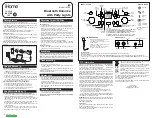
Listening to a tape / 

Audición de una cinta

7

Listening to the radio / 

Audición de la radio

Load a cassette into the cassette 

compartment.

Inserte un casete en el 

compartimiento del casete.

3

Press the POWER button to 

turn the power on.

Pulse el botón POWER para 

conectar la alimentación.

1

Press the TAPE button to select 

"TAPE 1" or "TAPE 2".

Pulse el botón TAPE para 

seleccionar "TAPE 1" o "TAPE 2".

2

TAPE 2

TAPE 1

Press the              button.

Pulse el botón             .

4

To stop the playback

Para detener la reproducción

Press the     button.

Pulse el botón      .

Press the TUNING (     /     )  button 

to tune in to the desired station.

Pulse el botón TUNING (      /     ) 

para sintonizar la emisora 

deseada.

3

Press the POWER button to 

turn the power on.

Pulse el botón POWER para 

conectar la alimentación.

1

Press the TUNER (BAND) button 

to select "FM ST" ,"FM"or "AM".

Pulse el botón TUNER (BAND) para 

seleccionar "FM ST", "FM", o "AM".

2

8

Recording from CDs / 

Grabaciones de discos CD

Press the POWER button to 

turn the power on.

Pulse el botón POWER para 

conectar la alimentación.

1

Press the TAPE (1     2) button to 

select the "TAPE 2".

Pulse el botón TAPE (1        2) para 

seleccionar "TAPE 2".

2

3

Press the REVERSE MODE button 

to select the reverse mode.

Pulse el botón REVERSE MODE 

para seleccionar el modo de 

inversión.

4

Press the CD button and load the 

desired disc.

Pulse el botón CD y coloque el 

disco deseado.

5

Press the NORMAL EDIT button.

Pulse el botón NORMAL EDIT.

6

•••••

  One side / 

Una cara

•••••

  Both side / 

Ambas caras

TAPE 2

Load a cassette into the 

TAPE2 cassette compartment.

Inserte un casete en el 

compartimiento del 

casete de TAPE 2.

To stop the recording

Para detener la grabación

Press the     button.

Pulse el botón      .

Summary of Contents for CD-C492

Page 1: ...et should be restored to its original condition and only parts identical to those specified be used SERVICE MANUAL This document has been published to be used for after sales service only The contents are subject to change without notice SHARP CORPORATION Manufactured under license from Dolby Laboratories Dolby Pro Logic and the double D symbol are trademarks of Dolby Laboratories Confidential Unp...

Page 2: ...posed metal cabinet parts and a known earth ground such as conduit or electrical ground connected to earth ground Use a VTVM or VOM with 1000 ohm per volt or higher sensitivity to measure the AC voltage drop across the resistor See diagram Connect the resistor connection to all exposed metal parts having a return path to the chassis antenna metal cabinet screw heads knobs and control shafts escutc...

Page 3: ...ter 0 15 WRMS Compact disc player section Type 3 disc multi play compact disc player Signal readout Non contact 3 beam semi con ductor laser pickup D A converter 1 bit D A converter Frequency response 20 20 000 Hz Dynamic range 100 dB 1 kHz Front speaker section Type 3 way 5 1 8 130 mm woofer 2 50 mm tweeter and super tweeter Maximum input power 80 W Impedance 8 ohms Dimensions Width 8 11 16 220 m...

Page 4: ...8 Dolby Digital Indicator 19 CD Play Indicator 20 CD Repeat Play Indicator 21 CD Pause Indicator 22 TAPE Record Indicator 23 Timer Record Indicator 24 Timer Play Indicator 25 Sleep Indicator 26 Extra Bass Indicator X BASS 27 CD Random Play Indicator 28 CD TUNER Memory Indicator 29 TUNER FM Stereo Indicator 30 TUNER FM Stereo Mode Indicator ST 31 Spectrum Analyzer Indicator 32 Function Selector But...

Page 5: ...n 51 CD Track Down Review Button TAPE 2 Fast Wind Button TUNER Tuning Down Button 52 TAPE 2 Reverse Play Button 53 CD Play Repeat Button TAPE 1 Play button TAPE 2 Forward Play Button 54 CD Track Up Cue Button TAPE Fast Wind Button TUNER Tuning Up Button 55 TAPE Normal Edit Button 56 TAPE High Edit Button 57 TAPE 1 Cassette Compartment 58 TAPE 2 Cassette Compartment 57 58 39 40 41 42 43 44 45 46 47...

Page 6: ...t Socket 4 DVD 2 VCR 2 Video Input Socket 5 Video Output Socket 6 CD Digital Output Socket Optical 7 VCR 1 AUX 1 Input Socket 8 VCR 2 AUX 2 Input Socket 9 FM 75 ohms Aerial Terminal 10 Aerial Earth Terminal 11 AM Aerial Terminal 12 AC Power Lead 13 Front Speaker Terminals 14 Centre Speaker Terminals 15 Surround Speaker Terminals 16 Sub Woofer Terminals CP C492 1 2 3 4 5 Front speakers 1 Super Twee...

Page 7: ...trol section 8 Track Up Cue Button 9 Track Down Review Button 10 Memory Button 11 Disc Skip Button 12 Stop Button 13 Play Repeat Button 14 Pause Button 15 Clear Button 16 Random Button Tape control section 17 TAPE 2 Record Pause Button 18 TAPE 2 Reverse Play Button 19 Stop Button 20 TAPE 1 Play Button TAPE 2 Forward Play Button 21 TAPE 2 Fast Wind Buttons Common section 22 Extra Bass Button 23 Equ...

Page 8: ... displayed Note In the event of a power failure or when the AC power cord is disconnected the clock display will go out When the AC power supply is restored the clock display will flash on and off to indicate the time when the power failure occurred or when the AC power cord was disconnected If this happens follow the procedure below to change the clock time To change the clock time When the unit ...

Page 9: ...oz de subgraves x 1 Surround speaker wire x 2 Cable de altavoz de sonido perimétrico x 2 Batteries are not included Las pilas no están incluidas Surround speaker Altavoz de sonido perimétrico Wall Pared 23 5 8 35 7 16 60 90 cm 60 90 cm 15 15 8 20 0 2m 6m 0 2m 6m 4 Connecting the system Conexión del sistema AC 120 V 60 Hz 120 V de CA 60 Hz TV TV Video Video Audio Optical Audio R R L L Video Audio C...

Page 10: ...ra conectar la alimentación 1 Press the CD button Pulse el botón CD Press the OPEN CLOSE button to open the disc tray and place the CD s on the disc tray label side up Pulse el botón OPEN CLOSE para abrir la bandeja del disco y coloque el disco s CD en la bandeja del disco con el lado de la etiqueta arriba 2 3 Press the OPEN CLOSE button to close the disc tray Pulse el botón OPEN CLOSE para cerrar...

Page 11: ...tón POWER para conectar la alimentación 1 Press the TUNER BAND button to select FM ST FM or AM Pulse el botón TUNER BAND para seleccionar FM ST FM o AM 2 8 Recording from CDs Grabaciones de discos CD Press the POWER button to turn the power on Pulse el botón POWER para conectar la alimentación 1 Press the TAPE 1 2 button to select the TAPE 2 Pulse el botón TAPE 1 2 para seleccionar TAPE 2 2 3 Pres...

Page 12: ...ution on Disassembly Follow the below mentioned notes when disassembling the unit and reassembling it to keep it safe and ensure excellent performance 1 Take cassette tape and compact disc out of the unit 2 Be sure to remove the power supply plug from the wall outlet before starting to disassemble the unit 3 Take off nylon bands or wire holders where they need to be removed when disassembling the ...

Page 13: ...0mm H1 x1 Front Panel K2 x1 ø3x10mm H2 x1 ø3x10mm K1 x2 K1 x1 H1 x1 Heat Shink Cover Power Amp PWB L1 x4 ø4x8mm L1 x1 ø3x10mm L1 x1 ø3x10mm Power Supply PWB N1 x3 ø3x10mm M3 x12 ø3x10mm Q1 x6 ø3x10mm Lug Wire P1 x1 ø3x10mm Open Headphones PWB Display PWB M1 x2 M2 x1 M2 x1 Washer Tape Mechanism Cassette Holder Left Right Front Panel CD Switch PWB S1 x1 ø3 x10mm S1 x1 ø3 x10mm R1 x1 ø3 x10mm Turntab...

Page 14: ...fore the disassembling method is not discribed For details refer to the disassembling drawing in the Parts Guide Be careful when installing the CD changer mechanism Install the CD changer mechanism on the CD player base after the shift lever has been set in the highest position Figure 14 1 Screw driver Woofer Woofer Net A1 x1 Baffle Board A2 x1 Tweeter Tweeter Super Tweeter A5 x2 ø3x10mm A3 x2 ø3x...

Page 15: ...e 15 2 REMOVING AND REINSTALLING THE MAIN PARTS CD MECHANISM SECTION Perform steps 1 2 3 18 and 20 of the disassembly method to remove the CD mechanism How to remove the loading motor See Fig 15 1 1 Remove the screws A1 x 2 pcs to remove the loading motor Figure 15 1 A1 x2 ø2 6 x5mm Loading Up Down Motor Motor PWB B1 x2 ø2 6 x6mm Shaft B2 x1 Stop Washer B3 x1 Gear B4 x1 CD Mechanism Pickup ...

Page 16: ... Adjusting Parts Instrument Connection 1 Input Antenna Output TP302 2 Input Antenna Output TP301 FM RF Signal generator 1 kHz 75 kHz dev FM modulated Band 87 50 MHz L303 fL 1 Coverage 3 7 V 0 1 V RF 98 00 MHz 98 00 MHz L302 2 10 30 dB Test Stage Instrument Connection Frequency Frequency Display Serring Adjusting Point Detection Signal generator 10 7 MHz FM sweep generator Detection 10 7 MHz 98 00 ...

Page 17: ...ng the optimal settings CD SECTION Figure 17 1 Note Only in STOP state it is possible to slide the pickup with the or key VOL Last memory BAL CENTER R GEQ FLAT X BAS OFF Canceling method POWER OFF Setting the test mode Any one of test mode can be set by pressing several keys as follows CD EQ POWER TEST CD operation test TEST mode Function CD test mode Setting of TEST mode Indication of CD TST mode...

Page 18: ...nt L R surround L R Center only monaural Front L R center Front L R When the surround mode is set to Normal or Phantom sound will also be heard from the surround speakers Front L R center surround monaural Front L R surround monaural Front L R center surround L R If a low frequency sound effect Low Frequency Effect contains a Dolby digital signal LFE will light in the display When this LFE is lit ...

Page 19: ...tion a tape is being played back indicates the record state 4 In the power section a tape is being played back 5 In the CD section the CD is stopped Parts marked with are important for maintaining the safety of the set Be sure to replace these parts with specified ones for maintaining the safety and performance of the set NOTES ON SCHEMATIC DIAGRAM Resistor To differentiate the units of resistors ...

Page 20: ...0 5ms 5 0 V HFL 0 5ms 5 0 V TES REVIEW 50ms 10 0 V JP CUE 50ms 10 0 V JP 50ms 0 50 V JP 50ms 1 00 V TE 0 5ms 10 0 V JP 0 5ms 10 0 V JP 0 5ms 0 50 V JP 0 5ms 1 00 V TE REVIEW 50ms 10 0 V JP 50ms 10 0 V JP 50ms 0 50 V JP 50ms 1 00 V TE 0 5ms 10 0 V JP 0 5ms 10 0 V JP 0 5ms 0 50 V JP 0 5ms 1 00 V TE PLAY 20ms 1 00 V SPO NORMAL DISC TN0 01 20ms 2 00 V CLV PLAY TCD 712 140mm TN0 01 50ms 1 00 V SPO 50ms...

Page 21: ...R IC1 LA9241M SERVO AMP 6 1 9 5 B1 12V B5 RES CQCK COIN SQOUT RWC WRQ CL DAT SELIAL CONTROL CE Q93 Q91 Q91 SL SL DRF 7 3 9 8 7 6 5 4 3 2 1 GND D MECHA UP GND D DISK NO OPEN CLOSE GND D M M GND M 9 8 7 6 5 4 3 2 1 CNP10 M 5V B1 62 64 45 36 23 43 31 24 25 10 10 26 58 53 10 12 20 32 40 43 44 53 52 51 54 31 30 29 23 27 16 15 41 44 Q1 Q52 4 3V Q81 7 3V B1 REGULATOR TO MAIN SECTION IC81 TA7291S LORDING ...

Page 22: ... 2 D3 GND D OUT D IN SL SR OUT SL SR IN ANAROG LCH 4 7 IN 2 1 6 7 IN 6 3 4 5 6 23 24 PWDA PWAD AINR AINR AINL AINL 2 8 18 19 20 22 25 1 7 9 10 21 B13 B9 AINR AINL AINL IN IN OUT OUT OUT ICA13 AK4520A A D D A CONVERTER ANAROG RCH ICA11 NJM4580M LOW PASS FILTER DIFFERENTIAL AMP A GND 8 4 2 1 8 B7 A GND A GND B7 ICA12 NJM4580M LOW PASS FILTER DIFFERENTIAL AMP 27 LS OUT RS OUT 26 VIDEO1 IN VIDEO2 IN M...

Page 23: ...9 29 37 44 53 65 68 71 D3 GND CENTER SUB WOOFER OUT IN IN OUT FL FR OUT ICA18 ZR38600 DOLBY AC 3 5 1 MPEG2 AUDIO DECORDER SUB WOOFER OUT FL FR OUT CENTER OUT SS SO SCK SI DEMO1 DEMO0 AC3 RESET SUB WOOFER ON OFF AD RESET 4 8 SUB WOOFER IN 4 5 6 12 13 QA03 11 10 A GND 7 14 QA01 QA02 B12 B12 8 1 9 2 5 7 B12 B7 ICA21 NJM4580M 15dB AMP SUB WOOFER OUT SUB WOOFER ON OFF SWITCHING FL FR VOLTAGE REGURATER ...

Page 24: ...IF CF301 FM OSC FM B Q344 B7 GND AM IF FM IF IN FM AM IF MPX AM MIX AM IF VCC IC241 MPX VCO ADJ FM DET VCO FM DET MO ST T351 FM IN AM IN IC302 TC72131 B7 B7 AM OSC IN AM B AM RF IN STEREO B7 5V MONO ST FM MONO ST REGURATER VOLTAGE PLL CONTROLLER OSC X352 4 5MHz FM AM DET OUT MPX IN FM B Q342 Q343 R L DI CL CE DO FMOSC FM SWITCHING FM AM IC QS7 QSO L B P F LA1805 T352 VR351 R L IN R IN L OUT R OUT ...

Page 25: ... L OUT R OUT C IN C OUT ICZ10 M62446FP 6 ch VOL SR IN SL IN SR OUT SL OUT SW OUT SW IN QY12 RELAY B6 STB RES TUNER MUTE TU DO TU SD T1 CrO2 T1 RUN T2 RUN T2 A FP T2 B FP 2 T2 CrO CAM SW TAPE SOL TA MOT HIGH SP FR SP BIAS TA R P PB EQ REC EQ REC MUTE REC MUT T1 T2 PB MUTE QS2AR QS2AC QS2MO FAN SP DET POSISTOR H P SW PROT FRONT RELAY SURROUND RELAY CENTER RELAY S W RELAY S MUTE POWER S W MUTE CENTER...

Page 26: ...2 13 14 1 2 3 4 5 6 1 2 3 4 5 6 1 2 3 4 5 6 1 2 3 4 5 6 CNS3A CNS3B CNP3A M M2 SLIDE MOTOR M M1 DISC MOTOR SW4 PICKUP IN 1 2 3 4 5 6 7 8 1 2 3 4 5 6 7 8 1 2 3 4 5 6 7 8 CNP2 CNS2B CNS2A 1 2 3 4 5 6 7 8 1 2 3 4 5 NC 49 50 51 52 53 54 55 56 57 58 59 60 61 62 63 64 NC CD2PUIN CD2GND B LD K PD A TR TR FO FO F E SL2 SP SP SL2 GND HF TP1 TE TBC JPCLO SLOF SLOF SLOF FSC FE1 FOSTA FSC EFBAL REF JP REF REF...

Page 27: ...NG SOLENOID 2 C51 100 16 9 8 7 6 5 4 3 2 1 1 2 3 4 5 6 7 8 9 10 11 12 13 14 CNP12 NC NC NC NC NC NC NC NC CD2LD2M M M SOL CD2LD2M CD2D2NO GND 7 3V TEST5 CS TA1 SOL GND M M M GND D OPEN CLOSE DISC NO GND D MECHA UP GND D 2Kx8 RAM 1BIT DAC SERVO COMMAND TES HLF V P CLV2 CLV TEST2 EFMIN EFMO VSS FR VVDD ISET VVSS PDO DEF1 CLV DIGITAL SERVO EXTERNAL OUTPUT SYNC DETECT EFM DEMODULATE SLICE LEVEL CONTRO...

Page 28: ...53 0 001 RP70 5 6K CP47 0 001 RP62 5 6K QP15 KTC3199 GR CP30 2 2 50 RP34 1K RP36 100K RP35 100K CP29 2 2 50 RP33 1K CP32 0 001 CP31 0 001 CENTER MUTE S W MUTE B 38 37 AC3 RS IN AC3 LS IN B B CR66 47 25 RR84 220 B RR83 220 CR65 47 25 RR19 47K CR15 4 7 50 RR21 47K CR17 4 7 50 QR11 KRA107 M QR13 KRA107 M RR20 47K CR16 4 7 50 QR12 KRA107 M VIDEO 2 VIDEO 1 1 2 3 1 2 3 1 2 3 47 46 45 31 32 33 28 29 30 S...

Page 29: ...A 4 6V D 15V A VGND 5V AC32A GND D3 GND D4 12V M VF1 VP VF2 VF1 VP VF2 4 6V D GND D 12V A 15V 5V AC32B RELAY4 GND M 12V M FAN SW RELAY3 VOL SW PROT POSISTOR OUT6 GND A OUT5 OUT4 AMP B CFWX11 TO SPEAKER AMP 1 PWB P42 1 B 15 12 11 10 9 8 7 6 5 4 3 2 1 13 14 FWP01 16 CFWP01 VOL SW FAN SW 12V M GND M GND A H P SW FAN CONT RELAY1 OUT1 L CH RELAY2 OUT3 OUT2 R CH SP LEVEL POSISTOR PROT AMP TO SPEAKER AMP...

Page 30: ... 67 68 69 70 71 72 73 74 75 76 77 78 79 80 81 82 83 81 82 83 84 85 86 87 88 89 90 91 92 93 94 95 96 97 98 99 100 98 99 100 GND A PL6 PL5 PL4 PL0 PL1 PL2 PL3 PC2 PC5 PC3 PC4 PC1 PC0 PB7 PB6 PB5 PB4 PB3 PB2 PB1 PA6 PA5 PA4 PA3 PA2 PA7 PB0 PA1 PA0 VDD1 CF2 CF1 VSS1 P74 P75 P07 P17 P16 P06 P05 P34 P35 P00 P01 P02 P03 P04 PCCL P30 P31 VSS3 VDD3 P32 P33 SCK SO1 SCK1 SO0 Si0 AN0 AN1 AN2 AN3 AN4 AN5 AN6 A...

Page 31: ...73 74 75 76 77 78 79 80 81 82 83 84 85 POWER SW RLY 4 REAR RLY 3 CENT RLY 2 S MUTE CENT MUTE REAR MUTE SWF MUTE AMP CONT VOLT SW SP PROT POSISTOR H P SW SP LEVEL FAN CONT FRNT RLY 1 QS2MO QS2AC GND A 12V A IN R IN L OUT L OUT R RR IN RL IN C IN RL OUT RR OUT C OUT QS2SPRED 12V M B B B B B 2 3 4 5 6 7 8 9 10 11 12 13 14 15 16 17 18 19 20 1 CFWU2 B B B B B A 12V AGND GND D3 VGND GND D4 A 15V SCK AC3...

Page 32: ...4 2 2K RK11 15K RK12 15K RK09 4 7K RK10 4 7K 8 7 19 5 4 3 2 1 17 18 20 21 22 23 24 6 CK05 330P CK06 330P RK89 1K RK90 1K CK16 47 16 CK15 47 16 CK14 330P RL13 6 8K QL12 KTA1266 GR RL12 2 2K RL14 33K RL11 33K QL11 KTA1266 GR RL15 10K QL14 KTA1273 Y CL12 47 16 RL17 10 1 2W QL15 KTA1271 Y DL12 1SS133 RL18 10K RL20 1 2K PHM1 FWM2 SWM4 REC RVS SOLM1 SOL SWM3 REC FWD SWM6 CAM SW SWM5 F A S VRM1 3 3K B RM...

Page 33: ...9 GR RK53 10K QK22 KTC3199 GR RK54 10K RK55 33K RK56 33K 12 13 14 15 9 8 7 11 10 16 17 8 RK60 270 RK61 270 CK62 0 047 ML RK66 27K RK42 82 RK40 560 RK63 10K CK55 0 022 CL13 3 3 50 RL24 3 3K 7 4 M QL18 KRC104 M QL19 KRC104 M QL16 KRC107 M DL11 1SS133 GND D PB MUTE GND A 12V A VCC GND HI SP HI SP HI SP BIAS T1_CRO2 TA_MOT_SW M_12V TA_CAM_SW T2_RUN T2_B_FP T1_RUN T2_A_FP M_GND TA_F R SPEED TA_SOL 3 1 ...

Page 34: ...0K RZ24 680 RZ16 120K RZ14 1M RZ18 680 RZ11 1M RZ05 1M RZ12 1M RZ06 1M RZ08 100K RZ39 330K RZ41 680 RZ33 330K RZ35 680 RZ27 270K RZ29 680 RZ21 120K RZ23 680 RZ15 120K RZ17 680 RZ07 100K RZ43 1K RZ44 1K RZ95 220 RZ09 100 RZ10 100 RZ45 1K RZ47 1K RZ49 1K RZ51 1K RZ46 1K RZ48 1K RZ50 1K RZ52 1K RZ62 10K RZ61 10K RZ93 1K RZ94 1K RZ87 470K RZ88 RZ90 22K RZ91 22K RZ38 1M RZ32 1M RZ26 1M RZ20 1M RZ37 1M ...

Page 35: ...8 9 10 11 12 13 14 15 16 17 18 19 20 21 2 2 3 2 2 4 2 5 6 2 27 28 29 30 31 32 33 34 35 36 37 38 39 40 41 42 39 38 37 36 35 34 115 116 117 118 119 120 121 OUT4 NC OUT3 NC OUT2 NC OUT1 NC SWIN GNDS SRIN SLIN GNDC GNDR C IN R IN L IN BYPASSR BYPASSL LTRE LBASS3 LBASS2 LBASS1 RBASS1 RBASS2 RBASS3 RTRE CR2 CR1 CL2 CL1 AVSS R OUT L OUT C OUT SL OUT SW OUT LA TCH DATA CLK SR OUT 7V C IN SWIN SRIN SLIN L ...

Page 36: ...5 47 25 CQ36 0 022 ML CQ04 2 2 50 CQ05 2 2 50 CQ03 2 2 50 CQ29 100 10 RQ05 1K RQ02 1K RQ01 1K RQ03 1K RQ04 1K CQ19 2 2 50 RQ13 1K RQ15 1K RQ11 1K RQ12 1K RQ14 1K RQ07 1K RQ06 1K RQ08 1K DQ01 1SS133 DQ02 1SS133 RQ20 100K RQ17 100K RQ18 100K RQ16 100K RQ19 100K 83 84 85 74 73 75 71 72 82 81 79 80 76 77 78 L CH IN R CH IN C OUT L CH OUT R CH OUT RR OUT RL OUT GND AU 12V A RL IN RR IN FLIN FRIN CIN SU...

Page 37: ... R380 1 5K C393 1 50 C338 100P 21 T352 R348 33K C314 10 16 C328 0 001 C392 0 001 1 IC301 TA7358AP FM FRONT END 12 R361 10K Q343 KRA109 M 11 9 C365 1 50 R357 3 3K 10 C366 1 50 R358 3 3K R364 47K C370 1 50 C354 470P Q342 KTC3199 GR TP302 R351 10K D342 1SS133 R369 4 7K R365 150 1 2W L343 100µH ZD351 MTZJ5 1B C369 47 16 R381 10K R362 470 C350 220 10 C349 0 022 C384 0 001 R350 47K R376 1K R356 10K C367...

Page 38: ...0 9 8 7 6 5 4 3 2 1 81 82 83 84 85 86 87 88 89 90 91 92 93 94 95 96 97 98 99 100 100 81 SWD03 X BASS SWD04 PRE EQ SWD12 TUNING UP CUE SWD13 STOP SWD14 NORMAL EDIT SWD15 HIGH EDIT SWD16 REC PAUSE SWD17 F PLAY SWD30 TUNING DOWN REWIND SWD31 CD PAUSE SWD32 REVERSE MODE SWD33 R PLAY SWD34 CLOCK SWD35 MEMORY SWD36 TIMER SWD05 MENU SWD06 ITEM SWD23 Q SOUND RE02 1K RE12 1K RE13 1 2K RE14 1 8K RE15 2 2K R...

Page 39: ...D VIDEO 1 SWD40 DVD VIDEO 2 SWD41 TAPE 1 2 SWD42 TUNER BAND SWD43 CD SWD48 POWER SWD30 NING DOWN REWIND RE21 8 2K RE11 8 2K RE31 8 2K E02 K E12 K RE42 1K RE43 1 2K RE44 1 8K RE45 2 2K RE52 1K E32 K RE41 8 2K RE51 8 2K RE01 8 2K 22 K RE53 1 2K SWD01 VOL JOG RD61 10K REMOCON VDD VSS JOG DOWN JOG UP VDD 29 VP XCOUT XCIN VOL JOG DOWN VOL JOG UP P32 P33 P34 P35 P36 P37 INT0 RES P74 P75 VSS1 CF1 CF2 VDD...

Page 40: ... 001 CB15 0 001 CB20 0 001 CA26 0 1 CB21 0 001 CB22 0 001 CB23 0 001 SDB VDD RESET SDA VDD SDE TCK SCK TDI SI GND SCKA WSA VDD WSB SDF D17 SCKB D16 SPFTX SDG D15 A0 GND SS TMS INT VDD D14 RDY GND A1 A2 A3 VDD D13 C D COAXIAL DIGITAL IN OPTICAL Vcc GND 1G B 1C3 1C2 1C1 1C0 1Y 2Y 2C0 2C1 2C2 2C3 A 2G GND Vcc VREFH VREFL AINR AINR AINL AINL VA AGND DIF1 DIF0 LRCK SCLK SDTI SDTO VCOM PWAD PWDA DGND VD...

Page 41: ...VDD SDB VDD RESET SDA VDD SDE TCK SCK TDI SI GND SCKA WSA VDD WSB SDF D17 SCKB D16 SPFTX SDG D15 A0 GND SS TMS INT VDD D14 RDY GND A1 A2 A3 VDD D13 C D D12 ERR A4 VDD GPIO5 GPIO4 GND A5 A6 D11 PP7 GPIO3 A7 A8 D10 PP6 A9 A10 GND VDD A11 VDD GND RD WR L CH R CH CKS DVDD DVSS XT0 XT1 PD BICK SDATA LRCK SMUTE DFS DEM0 DEM1 DIF0 DIF1 BVDD VCOM VREF DZF TTL AVSS AVDD Vcc GND L CH C CH SW CH DGND 3 3V DE...

Page 42: ...S133 QX15 KTC3199 GR RV38 10K RV37 47K QV16 KTC3199 GR 1 RV36 22K RV35 2 2K QV17 KTA1268 GR RV34 15K RV33 10K 2 DV21 1SS133 RV71 820 CV27 0 001 6 3 RV63 120K 1 2 14 RX37 47K RX38 10K QX18 KTC3199 GR RX55 10K CX27 0 001 6 3 RX33 120K RX35 2 2K RX36 22K RX34 15K QX17 KTA1268 GR DX21 1SS133 RX71 820 CV25 0 022 RV27 10K QV13 KTC3199 GR DV13 1SS133 RV69 0 2 1W RV28 10K QV14 KTC3199 GR DV14 1SS133 RV70 ...

Page 43: ...3 4 33 3 33 4 33 CV47 47 25 QV20 KTA1270 Y ZDV12 MTZJ6 2B RV56 3 9K QV21 KTC3199 GR DV20 1SS133 DV19 1SS133 DV25 1SS133 DV23 1SS133 DV24 1SS133 CV48 10 50 ZDV11 MTZJ5 1B RV59 100K RV58 10K DV22 1SS133 RV57 4 7K RV72 22K CV49 100 50 CV30 3300 50 CV29 3300 50 CX30 3300 50 CX29 3300 50 RV43 4 7 1 2W HP R CH HP L CH GND A H P SW M901 H P SW GND M RELAY1 RELAY2 RELAY3 RELAY4 FAN CONT FAN SW B TMV01 FRO...

Page 44: ...9 3 9 1 2W R920 3 9 1 2W C906 0 022 C901 0 022 C911 0 022 C915 0 022 C909 0 022 1 7 3V CD 12V A 12V M 4 6V D GND D GND M 5V AC3 CD GND D GND CD GND D VCC VCC VCC VCC GND VCC VCC GND GND GND VCC VCC GND GND CNS904 1 CNS903 2 3 4 5 6 7 2 3 4 5 6 7 1 1 2 3 4 5 6 7 2 3 4 5 6 7 BI903 BI904 CNPX12 TO SPEAKER AMP 1 PWB P42 6 H CNPV12 TO SPEAKER AMP 2 PWB P43 7 D B B B B 1 12 3V 22 7V 13 0V 12 8V 2 1V 35 ...

Page 45: ...50 ZD952 MTZJ6 8C Q951 KTA1266 GR D954 1N4004S R956 100 C965 100 35 R955 12K D953 1N4004S C962 47 63 OR 220 63 R957 2 2K D951 1N4004S C961 220 50 D952 1N4004S R954 220 R953 220 C960 220 50 C959 220 50 R951 1 R952 1 C957 0 047 ML C958 0 047 ML C966 0 047 ML C967 0 047 ML K991 K992 AC POWER CORD AC 120V 38V T F D992 D995 2A02 T991 POWER TRANSFORMER 60Hz D996 D999 1N4004S B POWER PWB D 1 FW901 2 3 VF...

Page 46: ...Q20 1 2 3 4 5 6 7 8 9 10 11 12 13 14 15 16 17 18 19 20 CQ19 CQ22 CQ26 ICQ01 RQ16 CQ16 CQ15 ZDQ01 CQ13 CQ10 CQ11 CQ06 CQ07 CQ08 CQ04 CQ03 CR12 RR14 RR12 DR12 DR11 CQ09 LR01 CR01 CR02 CQ12 ICR11 ZDZ02 RZ68 RZ65 RZ67 RZ66 RZ94 RZ93 RP91 RQ02 RQ01 RQ03 RQ05 RQ04 RQ11 RQ12 RQ17 RQ18 RQ09 RQ08 RQ07 RQ06 DQ01 DQ02 RQ19 RQ20 CQ02 CQ01 RQ10 RZ01 RZ86 CQ23 CQ28 CQ05 CZ31 RZ33 RZ63 CZ47 WTP1 WTP2 RZ64 CZ46 Q...

Page 47: ...2 QL11 RL11 QL17 QL13 QL18 RL16 RL15 RL18 RL17 QL14 QL15 RL19 QL19 QL16 WTL11 1 2 3 4 5 6 7 8 9 10 11 12 13 BIF12 1 14 RG22 RG19 CL13 CL12 RF98 RF95 RF92 RF91 RG04 QG01 RG29 CG01 DG05 QP17 QG92 E C B 1 2 3 RG08 RG07 RG06 RG37 BIF11 CNPP1 CNPF1 1 2 3 4 5 6 7 8 9 10 RZ86 RZ44 RZ43 CZ27 CZ28 RZ40 CZ24 RZ26 RZ30 RZ28 CZ16 RZ42 RF71 RF47 RG26 RF55 RF59 RF60 CZ29 ICZ06 RZ16 RZ38 2 ICZ04 CZ14 DL11 RZ12 Z...

Page 48: ...75 RA48 RA28 CA26 RA02 CA24 CA97 CA22 RA26 RA18 RA24 RA10 RA22 CA20 CA14 RA20 RA14 RA16 RA67 RA65 RA66 RA68 CA69 CA70 QH53 RA21 RA13 RA15 CA13 RA19 CA19 CH57 RH56 RH58 RH53 RB08 QH52 RA12 RA11 CH58 CH51 RH57 RH67 RH68 RH65 RH66 CH59 CH61 RA07 RH64 RH63 CH54 RH62 RH61 RA75 RA78 CA87 CA84 RA79 CH52 1 1 1 4 4 5 7 8 10 14 5 5 8 8 1 1 1 4 4 4 5 5 5 8 8 8 1 B H F 4 9 4 V 0 F 0 4 7 1 A W RA83 DOLBY PWB G...

Page 49: ...R12 C8 R11 C6 R14 R15 C9 R10 C5 R9 R8 C4 C54 CNP1 1 5 10 15 20 25 30 35 40 45 50 55 60 5 10 15 20 25 30 35 40 45 50 55 60 64 C15 R2 C1 C3 Q1 R1 C2 C33 R46 C31 C34 C32 R43 R40 R38 C30 R42 R39 C23 R52 R53 C48 C47 C38 C27 R41 C26 C40 R51 C39 D1 C28 C25 C57 C46 R47 R60 C37 XL1 IC2 C45 C42 C49 C44 R57 R58 R62 R59 R61 R63 R50 C22 R45 C29 C24 C41 C56 R44 IC1 17 1 2 3 4 5 6 7 8 1 2 3 4 5 6 1 2 3 4 5 16 49...

Page 50: ...DIT SWD14 NORMAL SWD13 STOP SWD23 Q SOUND SWD06 ITEM SWD05 MENU RD49 RD50 RD51 3 2 1 3 2 1 3 2 1 3 2 1 3 2 1 3 2 1 RD52 RD53 RD14 RD11 RD12 RE16 RE26 RE57 CD09 CD11 RD57 CD05 CD06 RD03 RD04 RD05 RD06 RD07 RD08 RD09 RD10 RD02 RD01 RE15 RE22 RE13 RE14 RE04 RD31 RD19 RD17 RD16 RD15 RD48 RE23 CD18 RD59 CD19 CD20 RE27 LD01 RD39 RE12 RV92 RV91 LV91 RE56 RD58 RD32 RD33 DD01 RE25 CD21 DD02 RD13 RE21 RD60 ...

Page 51: ...95 100 SWD43 CD SWD42 TUNER BAND SWD40 DVD VIDEO2 1 2 3 1 2 3 1 2 3 SWD39 DVD VIDEO1 SWD41 TAPE1 2 SWD38 CLEAR SWD35 MEMORY SWD31 CD PAUSE SWD29 BYPASS SWD34 CLOCK SWD37 SLEEP SWD36 TIMER RD55 RD14 RD45 RD12 RD54 RD28 RD71 RD70 RD72 RD35 RD36 RD27 RD26 RD22 RD21 CD01 RE53 RE52 RE38 RE35 RE11 E27 RE28 RE39 RE33 RE34 RE32 RE54 RE55 RE42 RE43 RD37 RD38 RD29 RD42 RD41 RD43 RD44 RE01 RD65 RE51 RD64 RE3...

Page 52: ...04 R913 R912 D905 R914 R952 1 2 3 R951 R954 R953 D993 ZD902 D951 D954 R956 R957 D952 D953 ZD951 R904 R906 D994 D995 ZD952 D992 R991 T F F990 T991 POWER TRANSFORMER BI904 BI903 R901 FW901 BI902 Q906 Q902 Q913 Q909 Q911 285 285 D991 C913 BI901 C919 1 7 1 7 F998 F997 2 5A F996 10A F995 10A 5A 1 6A RD WH WH WH WH WH WH WH WH WH WH WH WH WH WH RD 4 3 2 1 CNS902 7 6 5 4 3 2 1 7 6 5 4 3 2 1 CNPP02 TO MAI...

Page 53: ...304 C334 R323 VD301 2 C331 VD301 1 T302 D361 D362 C330 D302 L302 C310 D301 3 2 1 C309 C303 IC301 C302 C329 VR351 VCO 1 3 2 1 5 10 12 13 15 IC303 20 24 1 22 5 10 11 12 15 20 1 2 3 4 5 6 7 8 9 E C B 1 2 3 E C B 3 2 1 E C B TP303 TP302 TP301 TUNER PWB E CNSF13 P46 5 A TO MAIN PWB AM SO301 ANTENNA TERMINAL FM 75 OHMS BR COLOR TABLE RD R OR YL GR BL VL GY WH W BK PK BROWN RED ORANGE YELLOW GREEN BLUE V...

Page 54: ... QV22 RV61 RY22 QY12 QV18 QV19 RY59 RX50 DX17 RX40 QX20 TMX11 RY61 RV70 RX69 RX29 CNPV12 CV30 WTV11 ICX01 TMV01 ICV01 DV15 DV25 RV59 DV20 RX51 CY51 RY58 RY53 RY54 RX21 RV52 RV42 RV51 RV44 DV17 DY12 RY23 RV37 RV27 RV31 RV28 RV23 RX36 RX35 RX28 RX23 RY52 RX71 RX15 RX55 RX20 RX14 RX24 RX22 DV22 RV21 DV21 RV20 RV14 CY17 CY15 CX12 CX11 CY57 CX13 CX15 CY19 CX17 CV17 QV17 CV25 CV15 CX25 CX19 CY53 CY55 CX...

Page 55: ... Is from 5 V till 2 5V down pulse approx 300 ms Check the SW3 and the wiring from the ICF01 pin 84 to the SW3 No No input into the ICF01 pin 84 when the turntable is rotating 5V 2 5V 0V Yes Check IC2 pin26 Q91 and Q93 and the periphery Check the MECHA UP SW and the wiring from the ICF01 pin 85 to the MECHA UP SW No Yes Is there following voltage input on the ICF01 pin 84 in the specific state When...

Page 56: ... pins 24 and 25 IC81 pins 1 and 3 The CD function will not work The CD operating keys don t work Check the CD DSP power supply and 16 93 MHz clock and reset terminal Check the waveform of SCK SO DATA and SI COMM Yes Yes See if the pick up is the in PICKUP IN SW position If the items mentioned above are OK check the main microcomputer ICF01 Yes Yes No Yes No The CD operating keys work Check the Foc...

Page 57: ...Figure 57 2 Figure 57 1 Waveform in case of normal play back HF 1 0V DIV 0 5µsec DIV DC When playing back the disc 3 2 1 4 0 5s 1 00 V IC1 16 FD 0 5s 10 0 V IC2 13 CLV 0 5s 10 0 V IC1 54 DRF 0 5s 2 00 V IC1 7 TE Check the tracking system Check waveform of IC1 pin 7 TE Play is possible in TEST mode Although IL is possible play is impossible Check the periphery of IC 1 pin 14 Normal jump is impeded ...

Page 58: ...is performed when disc exits Yes Although HF waveform is normal TOC data cannot be read Yes Check PDO waveform Fig 58 Abnormal Check the IC1 pins 43 and 44 IC2 pins 3 5 7 10 and 11 Stop Play As VCO freque ncy is locked at 4 32 M Hz voltage of PDO rises and stabilizes 2 3 0 5s 1 00 V IC2 3 PDO 0 5s 1 00 V IC2 16 FD Although HF waveform is normal and the time indication is normal no sound is emitted...

Page 59: ...D Power terminal of digital system 24 CONT1 Input Output General purpose input output terminal 1 25 CONT2 Input Output General purpose input output terminal 2 26 CONT3 Input Output General purpose input output terminal 3 27 CONT4 Input Output General purpose input output terminal 4 28 CONT5 Input Output General purpose input output terminal 5 29 EMPH Output Difference monitor terminal At H deempha...

Page 60: ...put Input terminal for test Pull down resistor is integrated Surely connected to 0V 63 CS Input Chip selection input terminal Pull down resistor is integrated Connected to 0when not controlled 64 TEST1 Input Input terminal for test Pull down resistor is integrated Surely connected to 0V Pin No Note The same potential must be supplied to the power terminals VDD VVDD LVDD RVDD XVDD In this unit the ...

Page 61: ...nput 25 SPG Pin to connect gain setting resistor in the 12cm mode of spindle 26 SP Pin to connect spindle phase compensation constant together with SPD pin 27 SPD Spindle control signal output pin 28 SLEQ Pin to connect thread phase compensation constant 29 SLD Thread control signal output pin 30 SL Input pin of thread feed signal from micro computer 31 SL Input pin of thread feed signal from micr...

Page 62: ...Pin to connect capacitor for peak hold of RF signal 61 BH1 Pin to connect capacitor for bottom hold of RF signal 62 LDD APC circuit output pin 63 LDS APC circuit output pin 64 VCC1 RF system VCC pin Figure 62 BLOCK DIAGRAM OF IC 1 FIN2 FIN1 E F TB TE TE TESI SCI TH TA TD TD JP TO FD FD FA FA FE FE AGND SP SPI SPG SP SPD SLEQ SLD SL SL JP JP TGL TOFF TES HFL SLOF CV CV RFSM RFS SLC SLI DGND FSC TBC...

Page 63: ...r speaker signal out 19 FROUT Output Front right speaker out 20 FLOUT Output Front left speaker output 21 QXAC1 Input Capactior 22 QXAC2 Input Capactior 23 QXAC3 Input Capactior 24 QXAC4 Input Capactior 25 QXAC5 Input Capactior 26 QXBC1 Input Capactior 27 QXBC2 Input Capactior 28 QXBC3 Input Capactior 29 QXBC4 Input Capactior 30 QXBC5 Input Capactior 31 VANA Analog power supply 32 QXCC1 Input Capa...

Page 64: ...ment output terminal for LCD display S7 PA7 Usable as general purpose input output port PA 38 45 S8 PB0 Input OUtput Segment output terminal for LCD display S15PB7 Usable as general purpose input output port PB 46 53 S16 PC0 Input Output Segment output terminal for LCD display 53 S23 PC7 Usable as general purpose input output port PC 54 55 S24 PD0 Input Output Segment output terminal for LCD displ...

Page 65: ...e specified in 1 bit units 4 Bit input port Dual purrpose function P71 INT1 input HOLD release input P72 INT2 input timer 0 event input P73 INT3 input input with noise filter timer 0 event input 30 36 S0 T0 Output Fluorescent charcater display tube VFD display controller S6 T6 Segment timing shared output 37 45 S7 T7 Input OUtput Fluorescent charcater display tube VFD display controller S15 T15 Se...

Page 66: ...stand input port PF4 S45 High voltage withstand input port PF5 S46 High voltage withstand input port PF6 S47 High voltage withstand input port PF7 81 84 S48 S51 Input Output Fluorescent charcater display tube VFD display controller Segment output Dual purrpose function S48 High voltage withstand input port PG0 S49 High voltage withstand input port PG1 S50 High voltage withstand input port PG2 S51 ...

Page 67: ...ss bus The address bus is always active 26 D10 PP6 Input Output Data bus 27 A9 Output Address bus The address bus is always active 28 A10 Output Address bus The address bus is always active 29 GND Ground pin 30 VCC Used to connect a power supply of 3 3V 5 31 A11 Output Address bus The address bus is always active 32 D9 PP5 Input Output Data bus 33 D8 PP4 Input Output Data bus 34 SO Output Serial h...

Page 68: ...d D 80 SDB Output Data output for serial ports B C and D 81 VCC Used to connect a power supply of 3 3V 5 82 RESET Input Reset input Resetting is executed from the specified status and address by the reset signal 83 SDA Input Data input for serial ports A E and F 84 VCC Used to connect a power supply of 3 3V 5 85 SDE Input Data input for serial ports A E and F 86 TCK Input ICE interface clock JTAG ...

Page 69: ...t Interface Input FIFO 8X9 Memory Interfacce To PC optional ICE I F 4 XTAL DSP PLL Audio PLL GPIO 6 General Purpose I O Serilal Host I F Internal Data RAM 9KX20 To µ con 4 Internal Program RAM 1KX32 Internal Program Data ROM 16KX32 Digital Audio I F Transmitter Serial Audio Outputs Digital Audio I F output or Lt Rt output Serial Out LF RF LS RS C SW ZR38001 DSP CORE Figure 69 BLOCK DIAGRAM OF IC ...

Page 70: ... a h j k b f m g c e r p n d DP S6 S4 S5 S3 a h j k b f m g c e r p n d DP S6 S4 S5 S3 a h j k b f m g c e r p n d DP S6 S4 S5 S3 a h j k b f m g c e r p n d DP S6 S4 S5 S3 a h j k b f m g c e r p n d DP S6 S4 S5 S3 a h j k b f m g c e r p n d DP S6 S4 S5 S3 a h j k b f m g c e r p n d DP S6 S4 S5 S3 a h j k b f m g c e r p n d DP S6 S4 S5 S3 a h j k b f m g c e r p n d DP B7 B14 B21 B6 B13 B20 B5...

Page 71: ...ors parts codes Capacitors VCC Ceramic type VCK Ceramic type VCT Semiconductor type VC MF Cylindrical type without lead wire VC MN Cylindrical type without lead wire VC TV Square type without lead wire VC TQ Square type without lead wire VC CY Square type without lead wire VC CZ Square type without lead wire VC J The 13th character represents capacity difference J 5 K 10 M 20 N 30 C 0 25 pF D 0 5 ...

Page 72: ...N KTC3199 GR QG92 VSKTC3199GR 1 J AB Silicon NPN KTC3199 GR QH51 VSKTC3199GR 1 J AB Silicon NPN KTC3199 GR QH52 53 VSKRC102S 1 J AB Digital NPN KRC102 S QK3 6 VS2SC1845F 1 J AC Silicon NPN 2SC1845 F QK7 8 VSKTC3199GR 1 J AB Silicon NPN KTC3199 GR QK9 VSKTA1266GR 1 J AB Silicon PNP KTA1266 GR QK10 11 VSKRC104M 1 J AC Digital NPN KRC104 M QK15 16 VSKRC104M 1 J AC Digital NPN KRC104 M QK17 18 VS2SC28...

Page 73: ...CTYPA1CX104K J AB 0 1 µF 16V C13 VCKYMN1HB331K J AA 330 pF 50V C14 VCTYMN1CY103K J AA 0 01 µF 16V C15 VCTYMN1CY103N J AA 0 01 µF 16V C16 VCTYMN1CX472K J AA 0 0047 µF 16V C17 VCKYMN1HB102K J AA 0 001 µF 50V C18 VCEAZA1HW474M J AB 0 47 µF 50V Electrolytic C19 VCEAZA1HW105M J AB 1 µF 50V Electrolytic C20 VCEAZA1CW476M J AB 47 µF 16V Electrolytic C21 VCTYMN1CX332K J AA 0 0033 µF 16V C22 VCCSPA1HL221J ...

Page 74: ...F223Z J AA 0 022 µF 50V CA93 VCEAZA1HW225M J AB 2 2 µF 50V Electrolytic CA95 96 VCEAZA1EW476M J AB 47 µF 25V Electrolytic CA97 VCKYTV1EF104Z J AA 0 1 µF 25V CA98 VCEAZA1CW106M J AC 10 µF 16V Electrolytic CB1 2 VCKYTV1HB101K J AA 100 pF 50V CB3 4 VCKYTV1HF223Z J AA 0 022 µF 50V CB5 6 VCKYTV1HB221K J AA 220 pF 50V CB11 VCEAZA1EW476M J AB 47 µF 25V Electrolytic CB12 VCEAZA1AW107M J AB 100 µF 10V Elec...

Page 75: ...YPA1HF223Z J AB 0 022 µF 50V CX27 VCEAZA0JW108M J AC 1000 µF 6 3V Electrolytic CX28 VCEAZA1HW476M J AB 47 µF 50V Electrolytic CX29 30 VCEAZW1HW338M J AH 3300 µF 50V Electrolytic CX33 34 VCQYKA1HM473K J AB 0 047 µF 50V Mylar CY11 12 VCEAZA1HW225M J AB 2 2 µF 50V Electrolytic CY13 VCKYPA1HB471K J AA 470 pF 50V CY14 VCCSPA1HL470J J AA 47 pF 50V CY15 VCCSPA1HL150J J AA 15 pF 50V CY16 VCEAZA1HW107M J A...

Page 76: ...3 kohms 1 6W R909 VRD ST2CD102J J AA 1 kohm 1 6W R910 VRD ST2CD151J J AA 150 ohms 1 6W R911 VRD ST2EE561J J AA 560 ohms 1 4W R912 VRD ST2CD470J J AA 47 ohms 1 6W R913 VRD ST2EE561J J AA 560 ohms 1 4W R914 VRD ST2CD470J J AA 47 ohms 1 6W R917 VRD ST2EE472J J AA 4 7 kohms 1 4W R918 VRD ST2CD101J J AA 100 ohm 1 6W R919 920 VRD RT2HD3R9J J AA 3 9 ohms 1 2W R951 952 VRD ST2EE1R0J J AA 1 ohm 1 4W R953 9...

Page 77: ...kohm 1 8W RF83 VRD MN2BD103J J AA 10 kohm 1 8W RF84 86 VRD ST2CD102J J AA 1 kohm 1 6W RF87 88 VRD MN2BD102J J AA 1 kohm 1 8W RF91 VRD MN2BD102J J AA 1 kohm 1 8W RF92 VRD ST2CD102J J AA 1 kohm 1 6W RF93 94 VRD MN2BD102J J AA 1 kohm 1 8W RF95 VRD ST2CD102J J AA 1 kohm 1 6W RF96 97 VRD MN2BD102J J AA 1 kohm 1 8W RF98 99 VRD ST2CD102J J AA 1 kohm 1 6W RG4 8 VRD MN2BD103J J AA 10 kohm 1 8W RG11 VRD ST2...

Page 78: ... VRD RT2HD4R7J J AA 4 7 ohms 1 2W RV51 52 VRD RT2HD331J J AA 330 ohms 1 2W RV53 54 VRD ST2CD223J J AA 22 kohms 1 6W RV55 VRD ST2EE470J J AA 47 ohms 1 4W RV56 VRD ST2CD392J J AA 3 9 kohms 1 6W RV57 VRD ST2CD472J J AA 4 7 kohms 1 6W RV58 VRD ST2CD103J J AA 10 kohm 1 6W RV59 VRD ST2CD104J J AA 100 kohm 1 6W RV60 61 VRD ST2CD473J J AA 47 kohms 1 6W RV62 VRD ST2CD332J J AA 3 3 kohms 1 6W RV63 VRD ST2CD...

Page 79: ... FWM2 QCNWN0942AWZZ J AC Flat Wire 4Pin FWP1 QCNWN1218AWZZ J AF Flat Cable 16Pin FWP2 QCNWN1220AWZZ J AF Flat Cable 13Pin FWV91 QCNWN1281AWZZ J AG Flat Wire 5Pin JA11 QJAKZ0011AWZZ J AE Jack Digital 2 Coaxial JH51 QSOCJ0302AWZZ J AE Jack Video In Out JR11 12 QSOCJ0205AWZZ J AG Jack VIDEO AUX JV91 92LJACKH1759A J AF Jack Headphones M1 92LMTR1858CASY J AS Motor with Chassis Disc M2 92LMTR1854BASY J ...

Page 80: ... Front Panel Ass y 244 1 J Front Panel NotReplacement Item 244 2 PCUSG0022AWZZ J AB Cushion Leg 245 92LN BAND1318A J AA Nylon Band 80mm 246 LANGK0129AWFW J AF Bracket Fan Support 247 NFANP0001AWZZ J AD Rotary Fan 248 92LCSPR1431C J AA Ring Spring Fan 249 PRDAR0110AWFW J AY Heat Sink Main 250 92LMECHA2831A J BK Tape Mechanism Ass y 250 1 MM1 92LMTR2512AASY J AT Motor with Pulley Tape 250 2 NBLTH000...

Page 81: ...492 900 92L10002C49210 J BE Cabinet Ass y 901 92L200L0C49210 J BE Front Panel Left 901 92L200R0C49210 J BE Front Panel Right 903 92L201L0C49210 J AY Net Frame Ass y Left 903 92L201R0C49210 J AY Net Frame Ass y Right 905 92L23036099010 J AC Catching Holder 906 92L3141PC49210 J AM Speaker Cord Ass y 908 92L411B840160P J AD Screw 909 92L411B930100P J AC Screw 910 92L44010213500 J AH Port Cushion 911 ...

Page 82: ...CD C492 492C 80 11 A B C D E F G H 1 2 3 4 5 6 Figure 11 CD MECHANISM EXPLODED VIEW CD C492 492C 306 1 701 304 701 302 301 702 702 303 M1 703 305x2 SW4 M2 305 PWB K 306 2 306 3 306 704 ...

Page 83: ...04 607x2 611 611 611 x2 611 611 253 249 230 612 231 244 2 244 244 2 226 226 604 244 1 218 229 222 212 220 221 604 622 250 250 1 250 2 250 3 250 4 250 5 250 6 250 7 250 8 613 240 264 265 604x12 604x3 605x2 241 254 608x2 219 210 215 216 211 206 208 227 209 245 207 228 235 615 608 x22 613 PWB G PWB C3 PWB E PWB F1 PWB D PWB F2 PWB C2 PWB C1 217 223 224 213 225A 225B 225C 225 E 225D 223 1 223 2 223 3 ...

Page 84: ...2 492C PWB K CD MECHANISM PWB B 604 281 262 272 267 258 283 281 604 262 620x4 281 271 259 SOLM2 M3 602x2 SW2 268 278 266 274 276 277 277 263 603 617 275 273 617 280 279 281x2 281 612 257 281 281 SW3 201 619 616 261 260 1 260 2 260 3 260 282 609x2 609x2 202 203 205 204 604 618 270 269 13 ...

Page 85: ...3 905x2 905x2 SP3 4 909x2 911 SP1 2 908x4 910 Capacitor Capacitor 912 909x2 906 SP5 6 901 900 SUPER TWEETER SP5 L CH SP6 R CH TWEETER SP3 L CH SP4 R CH WOOFER SP1 L CH SP2 R CH SUPER TWEETER SP5 L CH SP6 R CH TWEETER SP3 L CH SP4 R CH WOOFER SP3 L CH SP4 R CH Capacitor 2 2µF BK YE BK BK RED RED ...

Page 86: ...CD C492 492C 84 A B C D E F G H 1 2 3 4 5 6 CP SW492 Figure 15 SPEAKER EXPLODED VIEW 2 3 15 RED BLACK 901 900 SP1 SP1 905x4 902 906 907 903 ...

Page 87: ... SP1 WOOFER SP7 SPEAKER TERMINAL 906 SPEAKER TERMINAL 906 TWEETER SP2 TWEETER SP8 YL BK BK YL RD 909x2 902 906 907 x2 911 908x3 SP1 904 907x2 900 908x6 908x2 SP2 Capacitor C1 901 SURROUND SP1 L CH SP2 R CH SPEAKER TERMINAL 900 909x4 910x2 901 SP1 L CH SP2 R CH SP3 L CH SP4 R CH 908 911 x2 909 x2 913x4 903 914 Capacitor C1 902 C1 2 2µF 100V WOOFER SP1 SP2 SPEAKER TERMINAL TWEETER SP3 SP4 ...

Page 88: ...oofer CP SW492 GBOXS0011AWM1 GBOXS0010AWM1 Rear Speaker L R Center Speaker A B C D D B C A FM AM Loop Antenna Quik Guide Operation Manual AC Power Supply Cord Remote Control FRONT BUTTON SIDE FRONT Speaker Cord x 2 Speaker Cord x 2 Rear Speaker Cord x 2 Center Speaker cord x 1 Not Replacement Item PACKING OFF THE SET For U S A Only Setting position of switches and knobs Tape Mechanism STOP COPYRIG...

Reviews: