background image

LC-60E77UN/LC-65E77UM/LC-C6077UN/LC-C6577UM

5 – 11

6. Special features

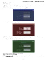
* STANDBY CAUSE (Page 1/40)

Display of a cause (code) of the last standby

The cause of the last standby is recorded in EEPROM whenever possible.

Checking this code will be useful in finding a problem when you repair the troubled set.

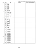
* EEP SAVE (Page 40/40)

Storage of EEP adjustment value

* EEP RECOVER (Page 40/40)

Retrieval of EEP adjustment value from storage area

7. Microcomputer software writing

7.1. Main microcomputer/monitor microcomputer software writing (Main PWB: QPWBXF282WJZZ)

7.2. Model/inch discrimination writing (Main PWB: QPWBXF282WJZZ)

• When writing the sub microcomputer software, the model data is configured with the software from the USB memory mounted to the checker.

• Reference and setting change are enabled through the process menu (Page 40/40) and RS-232C communication.

8. Signal adjustment

8.1. LCD section adjustment 1 [LCD module adjustment]

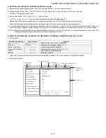
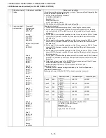
*2 Details of P1.10 (ERROR STANDBY CAUSE)

11

Prolonged unspecified-signal input in PC mode

in the cause of continuous “out of range”, PC input mode

17

Temperature error

in the cause of abnormal temperature

1A

Monitor trouble detected

in the cause of abnormal monitor mode

22

LCD controller Rom error

in the cause of software abnormality of LCD controller

Adjustment item

Adjustment conditions

Adjustment procedure

1

Software writing
Main/Monitor microcom-
puter software

Checker process

File version check
USB memory check

1. Connect the given jig to SC9301 (TL9301-TL9309, TL9311-TL9316) using the 
checker.
2. Connect the USB memory to J8001 (TL8003-8006) using the checker.
3. Apply the specified voltage to the main PWB and perform boot from the jig.
4.Send the software writing start command using RS232C.
5.Send the writing status check command and confirm the response of OK. Then 
turn off the power.

CAUTION: When the USB memory is not inserted or reading error occurs, nothing 

is written.

Adjustment item

Adjustment conditions

Adjustment procedure

1

Opposite bias adjustment. 
Left/Right
(LCD module adjustment 
item)

Adjustment in the center 
position of the panel

1. Enter the process mode using the process adjustment remote control.
2. Select [VCOM ADJ] using the Channel 

 keys on the remote control.

3. Press the Enter key to check that the pattern for adjustment is displayed.
4. Make adjustment so that the flicker located in the center of the screen is mini-
mized using the /- keys on the remote control.
5. If the status is optimized in step 4, press the Enter key to turn off the pattern.

CAUTION: * Make adjustment without ANT signal (since the active backlight 

changes the brightness).

[Adjustment position]

H/2

V/2

V/2

Summary of Contents for Aquos LC-65E77UM

Page 1: ...AJOR PARTS LC 65E77UM LC C6577UM 4 7 CHAPTER 5 ADJUSTMENT 1 ADJUSTMENT PROCEDURE 5 1 2 PUBLIC MODE SETTING PROCEDURE 5 18 CHAPTER 6 TROUBLESHOOTING TABLE 1 TROUBLESHOOTING TABLE 6 1 CHAPTER 7 MAJOR IC INFORMATIONS 1 MAJOR IC INFORMATIONS 7 1 CHAPTER 8 OVERALL WIRING SYSTEM BLOCK DIAGRAM 1 OVERALL WIRING DIAGRAM LC 60E77UN LC C6077UN 8 1 2 OVERALL WIRING DIAGRAM LC 65E77UM LC C6577UM 8 2 3 SYSTEM B...

Page 2: ...ng these checks Any reading of 0 75 Vrms this corresponds to 0 5 mA rms AC or more is excessive and indicates a potential shock hazard which must be corrected before returning the monitor to the owner SAFETY NOTICE Many electrical and mechanical parts in LCD color television have special safety related characteristics These characteristics are often not evident from visual inspection nor can prote...

Page 3: ... Brancher le cordon d alimentation directem ent à une prise de cou rant de 120V Ne pas utiliser de transformateur d isolation pour cet essai A l aide de deux fils à pinces brancher une résistance de 1 5 kΩ 10 watts en parallèle avec un condensateur de 0 15µF en série avec toutes les pièces métalliques exposées du coffret et une terre connue comme une conduite électrique ou une prise de terre branc...

Page 4: ...onventional lead solder by 40 C and as it has poor solder wettability you may be apt to keep the soldering bit in contact with the PWB for extended period of time However Since the land may be peeled off or the maximum heat resistance temperature of parts may be exceeded remove the bit from the PWB as soon as you confirm the steady soldering condition Lead free solder contains more tin and the end...

Page 5: ...CP SERVICE Software update OSD language English French Spanish Power Requirement AC 120 V 60 Hz Power Consumption 390 W 0 4 W Standby with AC 120 V 525 W 0 4 W Standby with AC 120 V Weight TV stand 92 6 lbs 42 0 kg 110 2 lbs 50 0 kg TV only 81 6 lbs 37 0 kg 99 2 lbs 45 0 kg Dimension 2 W x H x D TV stand 56 5 8 x 37 29 64 x 17 9 16 inch 60 3 4 x 39 27 32 x 17 9 16 inch TV only 56 5 8 x 35 11 64 x ...

Page 6: ...al PC IN AUDIO terminal shared for INPUT 4 and INPUT 6 4 Antenna Cable in INPUT 1 terminals INPUT 2 terminals AUDIO OUTPUT terminals LC 60E77UN LC C6077UN LC 65E77UM LC C6577UM AC INPUT terminal INPUT 3 terminals SERVICE terminal INPUT 5 terminal HDMI 1 2 3 1 1 External equipment connection 2 Button operations 3 Connecting the AC cord 4 Details on the PC Audio Select function The illustrations in ...

Page 7: ...nd AUDIO operation Indicator lights up for the current mode To enter the code registration mode you need to press FUNCTION and DISPLAY at the same time 18 LIGHT When this button is pressed some buttons for example VOL and CH on the remote control unit will light The lighting will turn off if no operations are performed within about 5 seconds This button is used for performing operations in low lig...

Page 8: ... time will start to keep appearing every minute Select Off by pressing SLEEP to cancel the sleep timer The TV will enter standby when the remaining time reaches 0 When the sleep timer is set its indicator on the TV lights red FLASHBACK Press FLASHBACK to switch to the previously tuned channel Press FLASHBACK again to switch back to the currently tuned channel FLASHBACK will not work if no channel ...

Page 9: ...ion Buttons AUDIO MTS SAP stereo mode The TV has a feature that allows reception of sound other than the main audio for the program This feature is called Multi channel Television Sound MTS The TV with MTS can receive mono sound stereo sound and Secondary Audio Programs SAP The SAP feature allows a TV station to broadcast other information which could be audio in another language or something comp...

Page 10: ...C This will present the Closed Caption information display 2 Press CC while the Closed Caption information is still on the screen Press repeatedly until you select the desired closed caption service Depending on the number of caption services in the signal being received you will see information such as 1 2 or 1 4 displayed 1 2 means the first of two services Example If a program has three service...

Page 11: ...and bottom of the screen Dot by Dot 1080i p only Detects the resolution of the signal and displays an image with the same number of pixels on the screen Full Screen 720p only You can select Full Screen only when receiving a 720p signal S Stretch Smart stretch Suitable for stretching 4 3 programs to fill the screen Zoom Suitable for viewing wide screen 2 35 1 aspect ratio programs in full screen Wh...

Page 12: ...APTER 3 DIMENSIONS 1 DIMENSIONS LC 60E77UN LC C6077UN Unit inch mm 5 5 16 135 4 45 64 119 4 45 64 119 2 41 64 67 7 21 64 186 17 9 16 446 15 3 4 400 15 3 4 400 3 15 32 88 52 17 32 1334 29 5 8 752 20 41 64 524 24 21 32 626 56 5 8 1438 35 11 64 893 2 9 32 58 37 29 64 951 AN 52AG4 ...

Page 13: ...NS LC 65E77UM LC C6577UM Unit inch mm 5 5 16 135 4 45 64 119 6 9 64 156 1 15 32 37 17 21 64 440 25 19 32 650 12 11 64 309 60 3 4 1543 56 13 32 1432 6 31 49 64 806 6 21 25 32 553 37 39 64 955 2 1 4 57 39 27 32 1012 24 21 32 626 17 9 16 446 4 45 64 119 AN 65AG1 ...

Page 14: ... OF MAJOR PARTS 1 REMOVING OF MAJOR PARTS LC 60E77UN LC C6077UN 1 Removing of Stand Unit and Rear Cabinet Ass y 1 Remove the 4 lock screws and detach the Stand Unit 2 Remove the 3 lock screws 1 lock screw 18 lock screws and detach the Rear Cabinet Ass y 2 Stand Unit Rear Cabinet Ass y 3 5 4 1 ...

Page 15: ...sconnect the KEY Unit from the KEY Button Cover Ass y and disconnect the connection cord from the KM Connector 4 Detach the R C LED Unit RA 5 Remove the 4 lock screws and 10 Hooks and detach the Front Cabinet Ass y 1 1 Speaker R Hook Speaker L Hook Front Cabinet Ass y LCD Panel Module Unit Ass y Hook Hook Hook Hook Hook Hook Hook Hook 4 R C LED Unit 3 KEY Unit 2 KEY Button Cover Ass y KM RA RA SP ...

Page 16: ...nect the following connectors from the MAIN Unit LB1 PD LP LW KM 3 Disconnect the following connectors from the LCD Control Unit and FPGA Unit LW PL LP 4 Disconnect the following connectors from the POWER Unit LA2 LA1 PD PL LCD Panel Module Unit Ass y 2 Side Terminal Cover Ass y 3 1 4 5 MAIN PWB Shield MAIN Unit POWER Unit LCD Control Unit FPGA Unit MAIN Unit POWER Unit LCD Control Unit FPGA Unit ...

Page 17: ... Unit 4 Remove the 4 lock screws and detach the LCD Control Unit 5 Remove the 2 lock screws and 4 lock screws and detach the Control PWB Angle 6 Remove the 8 lock screws and 1 hook and detach the POWER Unit 7 Remove the 4 lock screws and detach the POWER PWB Angle 16 POWER Unit 18 POWER PWB Angle 2 MAIN Unit 6 MAIN PWB Angle 15 4 12 3 5 Panel Lug 5 Panel Lug 11 9 7 8 FPGA Unit 10 LCD Control Unit ...

Page 18: ...emoving of VESA Angle and Support Angle 1 Remove the 20 lock screws and detach the 4 VESA Angle 2 Remove the 10 lock screws and detach the 2 Support Angle 2 VESA Angle 4 Support Angle 1 LCD Panel Module Unit Ass y 3 3 2 VESA Angle 4 Support Angle 1 1 1 ...

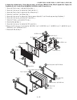
Page 19: ... Holder 44 Socket and 22 Lamp 5 Detach the Reflector Sheet 6 Remove the 12 lock screws and detach the INVERTER Cover L 7 Detach the INVERTER Unit 1 8 Remove the 12 lock screws and detach the INVERTER Cover R 9 Detach the INVERTER Unit 2 10 Detach the BL Chassis Ass y 2 9 14 13 6 2 5 10 12 15 8 5 4 11 7 6 3 1 Bezel Ass y Lamp Holder Socket BL Chassis Ass y INVERTER Unit 1 INVERTER Unit 2 INVERTER C...

Page 20: ...t and Rear Cabinet Ass y 1 Remove the 4 lock screws and detach the Stand Unit 2 Detach the 5 Spacers 3 Remove the 2 lock screws 1 lock screw 16 lock screws and detach the Rear Cabinet Ass y CAUTION In the case of assembly the new Spacer PSPAGA386WJ00 can be stuck on a screw 2 Stand Unit Rear Cabinet Ass y 1 4 3 3 3 5 6 ...

Page 21: ... R 3 Disconnect the KEY Unit from the KEY Button Cover Ass y and disconnect the connection cord from the KM Connector 4 Detach the R C LED Unit RA 5 Remove the 2 lock screws and 8 Hooks and detach the Front Cabinet Ass y Front Cabinet Ass y LCD Panel Module Unit Ass y Hook Hook Hook Hook Hook Hook Hook Hook 3 KEY Unit 2 KEY Button Cover Ass y KM RA SP 5 5 4 R C LED Unit RA 1 1 Speaker R Speaker L ...

Page 22: ...nect the following connectors from the MAIN POWER Unit LA PP1 PP2 PP3 PQ PL PD 4 Disconnect the following connectors from the SUB POWER Unit PP1 PP2 PP3 PQ 5 Disconnect the following connectors from the LCD Control Unit LW FR 4 1 3 2 Side Terminal Cover Ass y 5 MAIN PWB Shield LCD Panel Module Unit Ass y LCD Control Unit MAIN Unit SUB POWER Unit INVERTER 5 Unit INVERTER 2 Unit MAIN POWER Unit LC L...

Page 23: ... lock screws and detach the MAIN PWB Angle 3 Remove the 6 lock screws 3 Spacer and detach the MAIN POWER Unit 4 Detach the POWER2 Barrier 5 Remove the 8 lock screws 1 Spacer and detach the SUB POWER Unit 6 Detach the POWER1 Barrier 12 POWER1 Barrier 8 POWER2 Barrier LCD Panel Module Unit Ass y 9 10 5 1 11 SUB POWER Unit 4 MAIN PWB Angle 2 MAIN Unit 7 MAIN POWER Unit 6 3 ...

Page 24: ...f Corner Lug and Side Lug 1 Remove the 8 lock screws and detach the 4 Corner Lug 2 Remove the 4 lock screws and detach the 4 Side Lug 4 Side Lug LCD Panel Module Unit Ass y 1 1 1 1 3 3 3 4 Side Lug 2 Corner Lug 4 3 Side Lug 2 Corner Lug 2 Corner Lug 2 Corner Lug ...

Page 25: ...d detach the 2 Lamp Holder 7 Detach the 72 Socket and detach the 36 Lamp 8 Detach the Reflected Sheet 9 Remove the 5 lock screws and detach the LCD Control Unit 10 Remove the 29 lock screws and detach the INVERTER 1 Unit INVERTER 2 Unit INVERTER 3 Unit INVERTER 4 Unit INVERTER 5 Unit INVERTER 6 Unit 11 Detach the BL Chassis Ass y 26 23 19 18 20 17 24 25 21 22 19 13 14 16 12 13 14 15 1 10 5 3 6 2 1...

Page 26: ...RCCxxx USB and HLNRMxxx BIN The main software monitor microprocessor software can be upgraded by using a general purpose USB Memory The followings are the procedures for upgrading explained separately for the main software monitor microprocessor software 2 2 Main software version upgrade 2 2 1 Get ready before you start USB Memory of 128MB or higher capacity PC running on Windows 98 98SE ME 2000 X...

Page 27: ...s will trigger the upgrade failure screen NOTE In the event of a failure repeat the upgrade process If the process repeatedly fails it is likely that the hardware need fixing 6 Upon completion of the whole process the upgrade success screen as shown below appears You can check the new software version on this screen The version information appears after the upgrade is complete 7 Unplug the AC cord...

Page 28: ... may be serious damaged beyond recovery inability to start After the monitor microprocessor software is upgraded also perform the Industry Init 5 After the unit startup the upgrade starts The power led will blink continuously Also an upgrade screen will be shown during a minor upgrade 6 If the upgrade fails power led will stop blinking Also the upgrade failure screen will be shown if upgrade scree...

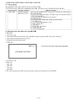
Page 29: ...ion described here lest your users should know how to enter the adjustment process mode If the settings are tampered in this mode unrecoverable system damage may result 4 Remote controller key operation and description of display in adjustment process mode 1 Key operation Input mode is switched automatically when relevant adjustment is started so far as the necessary input signal is available 2 De...

Page 30: ... Y coordinate setting for VIC READ 11 VIC COLOR Collected color data setting for VIC READ 12 VIC SIGNAL TYPE Signal type setting for VIC READ 13 VIC READ Picture level acquisition function Level appears in green on the upper right 3 1 N358 ALL ADJ INPUT1 CVBS and TUNER signal level adjustment 2 N358 ALL ADJ INPUT3 3 N358 MAIN ADJ INPUT1 CVBS signal level adjustment 4 N358 MAIN ADJ INPUT3 5 TUNER D...

Page 31: ...B adjustment value 7 MG3R WB adjustment Point 3 R adjustment value 8 MG3G WB adjustment Point 3 G adjustment value 9 MG3B WB adjustment Point 3 B adjustment value 12 1 MG4R WB adjustment Point 4 R adjustment value Parameter for six point adjustment 2 MG4G WB adjustment Point 4 G adjustment value 3 MG4B WB adjustment Point 4 B adjustment value 4 MG5R WB adjustment Point 5 R adjustment value 5 MG5G ...

Page 32: ...S Outout Gain 6 MVS Bass Gain 7 MVS FO 19 1 Bass CENTER ATT 2 Bass Vol0 MAX 3 Bass Vol60 MAX 4 Bass Vol60 CENTER 5 Bass Vol0 MIN 6 Bass Vol60 MIN 7 Treble CENTER ATT 8 Treble Vol0 MAX 9 Treble Vol60 MAX 10 Treble Vol60 CENTER 11 Treble Vol0 MIN 12 Treble Vol60 MIN 20 1 PEQ0 F0 2 PEQ0 Q 3 PEQ0 Gain 4 PEQ0 G Limit 5 PEQ1 F0 6 PEQ1 Q 7 PEQ1 Gain 8 PEQ1 G Limit 9 PEQ2 F0 10 PEQ2 Q 11 PEQ2 Gain 12 PEQ2...

Page 33: ... Vol OPT 6 Clip Level SP 7 Clip Level MON 8 Clip Level HP 9 Clip Level SW 10 Clip Level OPT 25 1 PANNEL SELECT 2 PWM 3 PWM FREQ 4 PWM DUTY 5 OSC FREQ 6 OSC DUTY 26 1 BRIGHTNESS DA0 2 BRIGHTNESS DA1 3 BRIGHTNESS DA2 4 BRIGHTNESS DA3 5 BRIGHTNESS DA4 6 BRIGHTNESS DA5 7 BRIGHTNESS DA6 8 BRIGHTNESS DA7 9 BRIGHTNESS DA8 10 BRIGHTNESS DA9 11 BRIGHTNESS DA10 12 BRIGHTNESS DA11 27 1 BRIGHTNESS DA12 2 BRIG...

Page 34: ...ADLEVEL 15 5 OPC33 ADLEVEL 16 6 OPC33 ADLEVEL 17 7 OPC33 ADLEVEL 18 8 OPC33 ADLEVEL 19 9 OPC33 ADLEVEL 20 10 OPC33 ADLEVEL 21 11 OPC33 ADLEVEL 22 31 1 OPC33 ADLEVEL 23 2 OPC33 ADLEVEL 24 3 OPC33 ADLEVEL 25 4 OPC33 ADLEVEL 26 5 OPC33 ADLEVEL 27 6 OPC33 ADLEVEL 28 7 OPC33 ADLEVEL 29 8 OPC33 ADLEVEL 30 9 OPC33 ADLEVEL 31 32 1 V6 OS THERMO 1 2 V6 OS THERMO 2 3 V6 OS THERMO 3 4 V6 OS THERMO 4 5 V6 OS T...

Page 35: ...DBY CAUSE4 5 ERROR STANDBY CAUSE5 6 ERROR STANDBY CAUSE RESET 40 1 EEP SAVE Writing setting values to EEPROM 2 EEP RECOVER Reading setting values from EEPROM 3 MODL NAME 4 PANEL SIZE 5 SETTING FOR ADJ 6 PANEL LIMIT 7 PANEL RANGE LIMIT 8 SHORT CHECK MODE 9 SHORT CHECK CURRENT 10 CURRENT SW Must be Low Don t change 1 Details of P1 9 NORMAL STANDBY CAUSE 2 No operation off in the cause of no operatio...

Page 36: ...or in the cause of software abnormality of LCD controller Adjustment item Adjustment conditions Adjustment procedure 1 Software writing Main Monitor microcom puter software Checker process File version check USB memory check 1 Connect the given jig to SC9301 TL9301 TL9309 TL9311 TL9316 using the checker 2 Connect the USB memory to J8001 TL8003 8006 using the checker 3 Apply the specified voltage t...

Page 37: ...on Adjustment Aging Common adjustment W B adjust ment top Vertical luminance difference adjustment bottom Composite signal 0 714Vp p 0 02Vp p Pedestal to white level 15K component signal Y level 0 714Vp p 0 02Vp p Pedestal to white level PB PR level 0 7Vp p 0 02Vp p 33K component signal Y level 0 7Vp p 0 02Vp p Pedestal to white level PB PR level 0 7Vp p 0 02Vp p Analog RGB RGB level 0 7Vp p 0 02V...

Page 38: ...r signal to the Video 4 analog RGB input 2 Automatic adjustment exe cution Point the cursor to ANALOG RGB ADJ and press the Enter key The adjustment is complete when ANALOG RGB ADJ OK is displayed Adjustment point Adjustment conditions Adjustment procedure 1 Setting NTSC RF signal US 7 AIR ch Send the NTSC signal to the RF antenna input 2 Automatic adjustment exe cution Point the cursor to TUNER V...

Page 39: ...ndard value 5 Set the point 3 to the specified gradation set the G correction value 1920 x G value of point 6 3712 fractions rounded off and adjust the RB so that it becomes the standard value 6 Set the point 2 to the specified gradation set the G correction value 944 x G value of point 6 3712 fractions rounded off and adjust the RB pattern so that it becomes the standard value 7 Set the point 1 t...

Page 40: ...Set the point 3 to the specified gradation set the G correction value 1680 x G value of point 6 3712 fractions rounded off and adjust the RB so that it becomes the standard value 6 Set the point 2 to the specified gradation set the G correction value 1136 x G value of point 6 3712 fractions rounded off and adjust the RB pattern so that it becomes the standard value 7 Set the point 1 to the specifi...

Page 41: ...heck 1 Enter the process mode 2 Point the cursor to EDID WRITE ENT and press the ENT key The writing is complete when ENT WRITE OK is displayed If not written HDMI does not function CAUTION Perform the data writing after setting the model discrimi nation The data based on the model discrimination infor mation is recorded in EEPROM 2 Analog RGB EDID writing Main PWB Inspection mode File version che...

Page 42: ...C6077 MDL C6577 MDL NOTE When replacing the main PWB make sure to perform the writing the inch and model name onto EEPROM Adjustment point Adjustment conditions Adjustment procedure 1 Factory setting Complete the setting by pulling out the AC cord Point the cursor to INDUSTRY INIT Cause set to ON using of the VOL key and press the ENT key The version confirmation screen appears on the green screen...

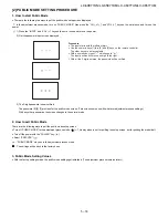
Page 43: ...ormal mode 2 How to exit Public Mode There are the following ways to quit the public mode setup screen Turn off PUBLIC MODE in the adjustment process mode This way alone is not for quitting the setup screen but for quitting the mode itself Turn off the power with the POWER key Select EXECUTE PUBLIC MODE stays on in the adjustment process mode The settings will be back to the factory ones 3 Public ...

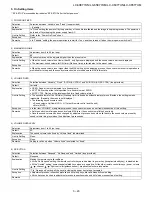
Page 44: ...y remote controller and VOL key remote controller and set To save new settings keep the cursor at EXECUTE and use ENTER key remote controller and set PUBLIC MODE POWER ON FIXED VARIABLE MAXIMUM VOLUME 60 VOLUME FIXED VARIABLE VOLUME FIXED LEVEL 20 RC BUTTON RESPOND PANEL BUTTON RESPOND MENU BUTTON RESPOND AV POSITION FIXED VARIABLE ON SCREEN DISPLAY YES INPUT MODE START NORMAL INPUT MODE FIXED VAR...

Page 45: ... at the level specified for a fixed volume at start Limit in Setting The sound volume for the ON timer Wake up timer is fixed also without display of menu Besides the setting is made impossible Basically the menu is not displayed The following keys become invalid Sound volume Up Down VOL for both remote control and the unit Mute MUTE Exception In the item VOLUME of adjustment process the sound vol...

Page 46: ...e cannot be displayed This is because the channel call mes sage may be confused with a message being sent from the hotel On the North America destined models the OSD works the same as at the No setting Limit in Setting Keys falling under any of the following items become invalid Appearance of screen changes and the sound changes Personal functions which are hard to restore Screen display menu OFF ...

Page 47: ...al Selection Selection between OFF ON TV RCE and ON TV RCD loop provided Default OFF Explanation Function to feed the remote controller received signal to Pin 9 open on the RS232C Limit in Setting None Exception None Remarks None Selection Selection between Variable and Fixed loop provided Default Variable Explanation In case of Fixed setting Menu Picture and Audio setting can t be changed like Dy...

Page 48: ...LIC MODE ON OFF Selection Selection between ON and OFF loop provided Default OFF Explanation In case of ON public mode settings are effected Limit in Setting None Exception None Remarks The public mode settings are operable only when this item is set at ON ...

Page 49: ... IC8001 CPU Check the line between pin 7 of input terminal J501 and pin AJ2 of IC8001 CPU Is there the COMPOSITE signal input at pin AE28 of IC8001 CPU Is there the COMPOSITE signal input at pin AE29 of IC8001 CPU YES NO YES NO Check the line between pin 8 of J507 and pin AE28 of IC8001 Check the line between pin 6 of J501 and pin AE29 of IC8001 Are the LVDS signal outputs at the LVDS 1st channel ...

Page 50: ...e the COMPONENT video signal inputs at pins AJ21 Y AJ22 Pb and AH22 Pr of IC8001 CPU Are there the COMPONENT video signal inputs at pins AJ18 Y AJ19 Pb and AH19 Pr of IC8001 CPU YES NO YES NO Check the line between the input terminals of J508 and IC8001 J508 pin 3 Y pin 5 Pb pin 7 Pr IC8001 pin AJ21 pin AJ22 pin AH22 Check the line between the input terminals of J502 and IC8001 J508 pin 3 Y pin 5 ...

Page 51: ...ne between pins 3 Y 4 C of J504 and pins AF30 AF29 of IC8001 Q519 and Q520 etc Are the LVDS signal outputs at the LVDS 1st channel and 2nd channel of IC8001 LVDS_TX_0_DATA0_P N C14 D14 LVDS_TX_0_DATA1_P N C15 D15 LVDS_TX_0_DATA2_P N C16 D16 LVDS_TX_0_DATA3_P N C18 D18 LVDS_TX_0_DATA4_P N C19 D19 LVDS_TX_0_CLK_P N C17 D17 LVDS_TX_1_DATA0_P N A14 B14 LVDS_TX_1_DATA1_P N A15 B15 LVDS_TX_1_DATA2_P N A...

Page 52: ...og video signal input at pin AD29 of IC8001 CPU Are there the video signal inputs at pin AA29 and AB29 of IC8001 CPU YES NO YES NO Check the line between IC8001 and TU1102 and their peripheral circuits Check the line between IC8001 and TU1102 and their peripheral circuits C1129 C1130 etc Are the LVDS signal outputs at the LVDS 1st channel and 2nd channel of IC8001 LVDS_TX_0_DATA0_P N C14 D14 LVDS_...

Page 53: ...17 R of IC8001 CPU Are there the VSYNC HSYNC signal inputs at pins AJ14 and AK14 of IC8001 YES NO Check the line between SC1804 and IC8001 IC1802 etc Are the LVDS signal outputs at the LVDS 1st channel and 2nd channel of IC8001 LVDS_TX_0_DATA0_P N C14 D14 LVDS_TX_0_DATA1_P N C15 D15 LVDS_TX_0_DATA2_P N C16 D16 LVDS_TX_0_DATA3_P N C18 D18 LVDS_TX_0_DATA4_P N C19 D19 LVDS_TX_0_CLK_P N C17 D17 LVDS_T...

Page 54: ... pin 41 of IC1605 and the pin 19 of SC1601 Check IC1605 and its peripheral circuits SDA1 pin53 of IC1605 SCL1 pin54 of IC1605 etc Check IC1605 and its peripheral circuits SDA1 pin53 of IC1605 SCL1 pin54 of IC1605 etc Are there the TMDS signal inputs at pins 1 2 CLK 3 4 D0 5 6 D1 7 8 D2 all of IC1605 Are there the TMDS signal inputs at pins 11 12 CLK 13 14 D0 15 16 D1 17 18 D2 all of IC1605 YES NO ...

Page 55: ... 41 of IC1801 and the pin 19 of SC1802 Check IC1801 and its peripheral circuits SDA1 pin53 of IC1801 SCL1 pin54 of IC1801 etc Check IC1801 and its peripheral circuits SDA1 pin53 of IC1801 SCL1 pin54 of IC1801 etc Are there the TMDS signal inputs at pins 65 66 CLK 67 68 D0 69 70 D1 71 72 D2 all of IC1801 Are there the TMDS signal inputs at pins 11 12 CLK 13 14 D0 15 16 D1 17 18 D2 all of IC1801 YES...

Page 56: ... FIXED Does the audio signal come from pins 5 L and 3 R of input terminal J507 to pins V30 L and V29 R of IC8001 CPU Does the audio signal come from pins 2 L and 4 R of input terminal J503 to pins U29 L and U28 R of IC8001 CPU YES NO YES NO Check the line between J507 and IC8001 Check the line between J503 and IC8001 Does the audio signal come from pins N29 N30 PGA0OUT_L R of IC8001 CPU to pins 4 ...

Page 57: ...ome from pins 5 L and 4 R of input ter minal J501 to pins U27 L and U26 R of IC8001 CPU YES NO Check the line between J501 and IC8001 Does the audio signal come from pins N29 N30 PGA0OUT_L R of IC8001 CPU to pins 4 7 INLP INRP of IC2701 AMP YES NO Check the line between IC8001 and IC2701 and their peripheral circuits Q1306 AMP_MUTE line etc Is the audio output from IC2701 as specified NO Check IC2...

Page 58: ...een Is the PC Audio Select selected for Input6 HDMI on the menu screen YES NO YES NO Set the HDMI audio output to Input4 PC Set the HDMI audio output to Input6 HDMI Is the HDMI audio output selected for Digital on the menu screen YES NO Set the HDMI audio output to Analog Does the audio signal come from pins 2 L and 3 R of input terminal J1801 to pins V28 L and V27 R of IC8001 CPU YES NO Does the ...

Page 59: ...tput selected for VARIABLE on the menu screen YES NO Set the audio output to FIXED Is there the SIF signal output at pin 14 of tuner TU1102 YES NO Check the tuner TU1102 and its peripheral cir cuits I2C line TUN_SCL TUN_SDA etc Does the SIF signal come from pin 14 of tuner TU1102 to pin D5 of IC8001 CPU YES NO Check the line between TU1102 and IC8001 and their peripheral circuits Q1101 Q1102 etc D...

Page 60: ...r to No external input video HDMI INPUT 5 INPUT 6 input If no video appears refer to No external input video HDMI INPUT 6 INPUT 7 input If no video appears refer to No external input video HDMI INPUT 7 INPUT 8 input If no video appears refer to No external input video HDMI INPUT 8 Is the audio output selected for VARIABLE on the menu screen YES NO Set the audio output to FIXED Does the audio signa...

Page 61: ...0 etc Is there the SPDIF signal input at pin 1 of D1306 OPTICAL OUTPUT YES NO Check the speakers and the optical cable Check D1306 and its peripheral circuits No optical output under the following conditions as per HDMI requirements Audio contents protected Audio frequency beyond 48kHz Audio bit length beyond 16bits No monitor audio output Is the audio output from the monitor set at VARIABLE or FI...

Page 62: ...of the accumulated counts Set LAMP ERROR RESET on page 2 of the process A to 0 Power error Flashes twice H On L Off Refer to Power error details Communication error with the main CPU Flashes 3 times H On L Off Refer to Communication error details Communication line error or main CPU communication error Check debug statements for the main CPU Communication line with the main CPU TxD 28pin RxD 29pin...

Page 63: ...n 1 cycle Basically log analysis of debug print statements or com munication log analysis by a bus monitor is performed Initial communication reception error Flashes once H On L Off Initial communication from the main CPU is not received Request for the monitor model No is not received after cancel ing the reset Communication line error or main CPU start up failure Time out setting reception error...

Page 64: ...h recovered clock and carrier timing filters and equalizes the data and passes soft deci sions to an ATSC A74 and ITU T J 83 Annex B compatible decoder It has an MPEG 2 Digital Video Broadcasting DVB compliant transport processor with advanced section filtering capability DVB descrambler and an MPEG 2 MP HL profile video decoder Audio support includes a BTSC and a Dolby AC3 MPEG 2 Layer 1 2 audio ...

Page 65: ...Z Full HD Panel 㧔1920 1080㧕 60 R1LK600D3GW10Z Inv Unit Inv Unit MAIN Unit F282 MDK V LR HDMI USB DDR Position ޣ RA ޤ 1 10 1 4 ޣ SP ޤ RS 232C Analog RGB PC Audio IN ޣ LW ޤ 1 41 ޣ PD ޤ 1 12 ޣ KM ޤ 1 4 TUNER ޣ LP ޤ 1 15 1 9 1 21 ޣ LB ޤ POWER Unit RDENCA369WJQZ 60 Plaice FPGA 1 41 Inv Unit Inv Unit 1 14 1 10 1 10 Synchronized signal ޣ LC ޤ ޣ LC ޤ 1 12 1 10 1 4 ޣ PD ޤ ޣ LA1 ޤ ޣ PL ޤ ޣ LA ޤ ޣ LA2 ޤ 1 80...

Page 66: ...AIN Unit F282 HDMI Optical Output MDK V LR HDMI USB DDR Position ޣ RA ޤ 1 10 1 4 ޣ SP ޤ RS 232C Analog RGB S video Terminal PC Audio IN ޣ LW ޤ 1 41 ޣ PD ޤ 1 12 ޣ KM ޤ 1 4 TUNER ޣ LP ޤ 1 15 1 9 1 21 ޣ LB ޤ SubPower Unit 65 㧦RDENCA323WJQZ 65 Arugula 1 41 1 12 ޣ FR ޤ 1 80 1 80 Inv Unit Inv Unit Main Power Unit 65 㧦RDENCA324WJQZ ޣ PD ޤ 1 12 1 4 1 9 1 12 1 12 Synchronized signal 1 6 1 3 1 3 ޣ LC ޤ ޣ LC...

Page 67: ...7WH126FU WP RGB_L R LR Audio Out I O OPTICAL OUT CPU_SPDIF_OUT RST_FLS_CPU RS_BUF_CNT CNVss RxD TxD 27 000MHz X8001 X tal 20MHz Xtal 20MHz IC2004 EEPROM S24CS08J BU 3 3V N_DBG_RST I2C1 400KHz INPUT 7 INPUT 6 INPUT 4 LR Component RF IN TU1102 Analog Digital Tuner D_IF AGC I2C 3 3V TxD RxD STB DET_PNL12V I2C_0 100KHz 5V TUNER_I2C TUNER_I2C 100KHz 5V 3 3V IC2001 Reset BU 3 3V J8001 USB PNL_ON From CP...

Page 68: ... C LED Unit Unit 1 2 3 10 9 7 6 5 4 8 J A B C D E F G H I 13 11 19 18 16 15 14 12 17 KEY Unit Side A KEY Unit Chip Parts Side A R C LED Unit Side A R C LED Unit Chip Parts Side A S155 R153 D152 S154 S152 R151 D151 S151 R152 S153 R154 S156 S157 D155 P151 S155 R153 D152 S154 S152 R151 D151 S151 R152 S153 R154 S156 S157 D155 P151 ...

Page 69: ...LC 60E77UN LC 65E77UM LC C6077UN LC C6577UM 9 2 2 MAIN Unit 1 2 3 10 9 7 6 5 4 8 J A B C D E F G H I 13 11 19 18 16 15 14 12 17 Main Unit Side A ...

Page 70: ...520 C9504 R510 C9505 C1805 FB521 FB9001 R511 C9506 R512 C1806 FB522 FB9002 R8157 C1807 FB9003 FB523 R8158 FB9004 C1808 R514 Q1805 R515 C1809 IC8152 R516 Q1806 IC8153 Q1807 Q1617 Q1618 C1810 P2001 C1811 P2002 C1812 P2003 Q9703 C1813 Q9704 C1814 C1621 C1622 R522 C1816 Q1812 C1818 R526 C1629 SC9001 R529 R9303 R9304 R1604 C1820 L1101 C1821 L1102 C1822 L1103 C1823 R9308 C1824 L1105 IC1601 D9501 IC1602 ...

Page 71: ...LC 60E77UN LC 65E77UM LC C6077UN LC C6577UM 9 4 1 2 3 10 9 7 6 5 4 8 J A B C D E F G H I 13 11 19 18 16 15 14 12 17 MAIN Unit Side B ...

Page 72: ...80 Q1610 C1614 Q1804 C9509 C8181 C1615 TL549 Q1611 C8182 C1616 Q1612 C8183 C1617 Q1613 C8184 C1618 Q1614 Q1808 C8185 C9701 C1619 Q1615 Q1809 C8186 Q1616 C9702 C8187 C9510 C8188 TL550 Q1619 C9511 C8189 Q9701 TL551 C9512 Q9702 TL552 TL553 C9513 C1620 Q1810 C9709 Q9705 C1815 Q9706 Q9707 C1623 Q1813 C1817 Q1620 C1624 C8190 Q1814 C1625 D1601 C8191 D9301 TL559 C1819 C1626 D9302 D1602 C1627 D9303 Q1817 D...

Page 73: ... capacitors are µF unless otherwise noted P pF µµF 2 All capacitors are 50V unless otherwise noted CAUTION This circuit diagram is original one therefore there may be a slight difference from yours SAFETY NOTES 1 DISCONNECT THE AC PLUG FROM THE AC OUTLET BEFORE REPLACING PARTS 2 SEMICONDUCTOR HEAT SINKS SHOULD BE REGARDED AS POTENTIAL SHOCK HAZARDS WHEN THE CHASSIS IS OPERATING IMPORTANT SAFETY NO...

Page 74: ...75SG C1119 0 047u 10V R1107 0 CZ C1118 1000P 50V TAR5SB33 1 VIn 2 GND 3 ON 4 Nr 5 Vout SIF R1115 100 LUG1104 HA006WJ SIF_CM LUG1105 HA006WJ R1134 0 CY R1141 0 CY R1142 0 CY R1123 0 C1141 1000P 50V C1142 1000P 50V C1143 1000P 50V C1152 10u 10V KZA616WJQZ R1152 0 C1153 10u 10V KZA616WJQZ LV5893M 3 9V 1 BS 2 Vin 3 SW 4 GND 5 FB 6 COMP 7 EN 8 SS R1148 10K F D1102 RB056L40 VHD C1147 0 1u CYB 25V R1147 ...

Page 75: ...5P CH C517 15P CH R592 100K 0 15uH L505 PMT C523 15P CH 0 15uH L504 PMT C522 15P CH R589 100K 0 15uH L503 PMT C504 15P CH R588 100K 0 15uH L506 PMT R559 0 CZ C519 15P CH R561 0 CZ C505 15P CH C514 15P CH C537 470P CH C508 15P CH 0 15uH L502 PMT C539 470P CH Q519 KTC3875SG C509 15P CH C521 15P CH C533 470P CH C520 15P CH C516 15P CH C506 15P CH C525 15P CH Q520 KTC3875SG C507 15P CH 0 15uH L501 PMT...

Page 76: ...OUT_R PGA1OUT_L 10u 10V C1309 KZA616WJQZ R1345 15K R1339 2 2K R1340 560K R1342 560K LINE_OUT_L LINE_OUT_R C1306 1u 16V R1334 1K C1307 1u 16V R1310 1K LA79200V EXP I O 1 VCC 2 DA0 NC 3 DA1 NC 4 NC NC 5 IO7 6 IO6 7 IO5 8 IO4 9 GND 10 IO3 11 IO2 12 IO1 13 IO0 14 ADDR 15 SCL 16 SDA R1328 4 7K 1 2 3 4 5 6 7 8 D3 3V R1305 0 C1314 10u KZA098WJ 25V D1301 KDS4148 VHD Q1312 KRC404E R1333 22K C1310 0 1u 25V ...

Page 77: ...25V R2726 0 R2731 0 R2741 75K C2713 0 1u 25V R2715 220K F R2717 27K Q2704 KRC404E VS R2752 220K F R2742 20K R2754 22K F R2753 68K F C2748 100P R2719 5 6K P2701 NA160WJ To EX SP 1 RCH 2 RCH 3 LCH 4 LCH UR13V FB2706 A206WJ GND_B C2712 10u 10V KZA616WJQZ YDA148QZ 1 PVDDREG 2 AVDD 3 INLP 4 ILM 5 VREF 6 INRM 7 INRP 8 AVSS 9 PLIMIT 10 PVDDPR 11 OUTPR 12 OUTPR 13 PVSSR 14 OUTMR 15 OUTMR 16 PVDDMR 17 SLEE...

Page 78: ...116WJ 1 2 3 4 L1603 FA116WJ 1 2 3 4 L1604 FA116WJ 1 2 3 4 SC1601 ZA149WJQZ TMDS Input1 Side Type 1 2 3 4 5 6 7 8 9 10 11 12 13 14 15 16 17 18 19 20 21 22 23 C1618 0 1u C1620 1000P TC7SH17U Shumit Buffer 1 NC 2 IN 3 GND 4 OUT 5 VCC C1623 0 1u 10V SII9287 1 R1XCN 2 R1XCP 3 R1X0N 4 R1X0P 5 R1X1N 6 R1X1P 7 R1X2N 8 R1X2P 9 VCC33 10 RSVD 11 R2XCN 12 R2XCP 13 R2X0N 14 R2X0P 15 R2X1N 16 R2X1P 17 R2X2N 18 ...

Page 79: ... R3X1N NC 24 R3X1P NC 25 R3X2N NC 26 R3X3P NC 27 VCC33 28 RSVD 29 DSDA0 30 DSCL0 31 HPD0 32 R0PWR5V 33 DSDA1 34 DSCL1 35 HPD1 NC 36 R1PWR5V 37 MICOM_VCC33 38 SBVCC NC 39 DSDA2 40 DSCL2 41 HPD2 42 R2PWR5V 43 DSDA3 44 DSCL3 45 HPD3 NC 46 R3PWR5V 47 DSDA4 48 DSCL4 49 R4PWR5V 50 CEC_A NC 51 CEC_D NC 52 INT 53 CSDA 54 CSCL 55 TPWR_CI2CA NC 56 TX2P 57 TX2N 58 TX1P 59 TX1N 60 TX0P 61 TX0N 62 TXCP 63 TXCN...

Page 80: ...17 TD2 18 TCLK2 19 TCLK2 20 GND 21 TC2 22 TC2 23 TB2 24 TB2 25 TA2 26 TA2 27 GND 28 TE1 29 TE1 30 TD1 31 TD1 32 TCLK1 33 TCLK1 34 GND 35 TC1 36 TC1 37 TB1 38 TB1 39 TA1 40 TA1 41 GND C2602 0 1u 10V R2620 0 OPWM1 FB2609 A204WJ DET_SYNC R2639 100K FB2614 A074WJ FB2616 A074WJ FB2617 A074WJ FB2620 A074WJ FB2621 A074WJ FB2622 A074WJ FB2623 A074WJ FB2624 A074WJ FB2625 A074WJ FB2626 A074WJ FB2627 A074WJ ...

Page 81: ...C 16 P8_4 17 ACCESS_G NC 18 DET_SYNC 19 ILL_LED 20 AV_LINK_O NC 21 MUTE_A_ALL 22 CEC_O 23 IRPASS 24 CEC_O2 25 DET_COND 26 W_PROT_M 27 I2C_SCL 28 I2C_SDA 29 TXD 30 RXD 31 SCLK 32 BUSY 33 DET_POW0 34 DET_POW1 35 DET_POW2 36 DET_POW3 37 DET_POW4 NC 38 DET_POW5 NC 39 EPM 40 ERR_PNL 41 MODEL_A4 NC 42 MODEL_A3 NC 43 MODEL_A2 NC 44 CE 45 TXD_DBGP 46 RXD_DBGP 47 EXE_LED NC 48 N_SYSTEM_RST NC 49 STB 50 FRA...

Page 82: ... F R8003 100 F S1_PLG CNVss C1_PLG RS_BUF_CNT PM_REQ C2_PLG V1_PLG RST_FLS_CPU CBOOTS V3_PLG STB_CPU I2CEXT OPWM1 CPU_UARXD0_RS CPU_UATXD0_RS PNL_ON SMPOWHOLD RC DDR_BA2 R8018 0 R8020 0 N_CPU_RST R8037 30K R8038 30K R8031 30K R8032 30K R8033 30K R8034 30K R8035 30K R8036 30K CPU_SPDIF_OUT C8040 0 1u 10V C8041 0 1u 10V C8042 0 1u 10V C8043 0 1u 10V C8044 0 1u 10V C8045 0 01u 25V C8039 4 7u 10V KZA0...

Page 83: ...A4 R8154 0 N_DDR_CS0 DDR_DQS3 C8184 10u 10V KZA616WJQZ DDR_A10 C8183 0 1u N_DDR_WE DDR_A11 DDR_DQM1 DDR_BA0 DDR_DQ7 DDR_DQ9 DDR_DQ12 DDR_DQ29 DDR_CK1N N_DDR_DQS0 D1 8V N_DDR_DQS3 DDR_DQ1 DDR_DQ18 DDR_DQ10 DDR_DQ20 C8179 0 1u DDR_DQ30 DDR_ODT0 DDR_A2 DDR_DQ0 DDR_A9 DDR_DQM0 DDR_DQ24 DDR_DQ13 IC8153 IXC768WJQZ DDR2 MEMORY 512Mbit 1066M A1 B1 C1 D1 E1 F1 G1 H1 J1 L1 N1 R1 R2 R3 NC R7 NC R8 NC P9 M9 K...

Page 84: ...C 16 CLE 17 ALE 18 WE 19 WP 20 NC 21 NC 22 NC 23 NC 24 NC 25 NC 26 NC 27 NC 28 NC 29 I O0 30 I O1 31 I O2 32 I O3 33 NC 34 NC 35 NC 36 VSS 37 VCC 38 NC 39 NC 40 NC 41 I O4 42 I O5 43 I O6 44 I O7 45 NC 46 NC 47 NC 48 NC R8451 47 R8455 4 7K PACLE N_PARB PDD6 N_POWE PDD5 PDD4 PDD2 PDD7 PAALE PDD3 R8458 0 1 2 3 4 5 6 7 8 R8459 0 1 2 3 4 5 6 7 8 C8456 0 1u CZB R8453 4 7K R8463 0 R8462 0 N_POCE1 TO MAI...

Page 85: ...08W 1 2 3 GND 4 5 Vcc R9305 4 7K CZ SMPOWHOLD R9319 4 7K CZ N_CPU_RST R9301 47K CZ D9304 1PS184 1 2 3 N_SRESET C9301 0 1u 10V GND_B R9302 3 3K CZ D3 3V R9308 4 7K CZ OPWM2 R9326 1K CZ TO MAIN9 CPU PWBXF282WJ TO MAIN8 UCOM TO MAIN14 POWER1 TO MAIN9 CPU TO MAIN9 CPU 12 16 IC9301 DUNTKF282WE06 07 11 MAIN12 EXBUS MAIN UNIT 12 16 3 2 0 0 2 8 ...

Page 86: ...R9020 100 TVN 1 10W FB9003 A192WJ TC7W00U 1 2 3 4 GND 5 6 7 NC 8 VCC RC D9005 MAZ9120H 1 2 3 NC FB9001 A042WJ R9002 10K IRPASS C9003 0 1u CZF 25V Z D9002 MA111G C9004 0 1u CZB 10V C9010 0 1u CZB 10V K RS_ON R9027 4 7K R9028 4 7K R9025 4 7K R9026 4 7K SDA1 SCL1 R9015 10K C9007 0 1u CYB C9001 10u 16V KZA510WJPZ C9006 0 1u CYB M3221EIP 1 N_EN 2 C1 3 V 4 C1 5 C2 6 C2 7 V 8 RIN 9 ROUT 10 NC N_INVALID 1...

Page 87: ...9616 12K F C9605 1u 10V KZA520WJQZ C9626 4 7u 10V KZA067WJ R9603 2 7K F R9607 470 J C9603 3300P CZB R9605 5 6K R9601 10K F D3 3V R9629 39 CZ R9630 1 TWF 1 2W R9631 1 TWF 1 2W A3 3V 350mA R9633 39 R9634 4 7 C9635 2200P CZB MM3443DF 1 Vout 2 NC 3 GND 4 NC 5 CE 6 Sub 7 Vin D9603 MA111G VHD D9609 MA111G VHD R9613 10K F Q9602 RT1N141U VS R9618 2 7K F Q9603 KTC3875SG VS D1 1V 0 8V D1 8V START R9608 4 7K...

Page 88: ...25V KZA104WJ R9702 10K CZ R9701 22K CZ A8V 5V 5V 5V UR13V FB9708 A375WJQZ FB9709 A074WJ FB9706 A375WJQZ FB9712 A375WJQZ FB9710 A074WJ FB9707 A375WJQZ FB9711 A375WJQZ FB9702 A375WJQZ FB9704 A375WJQZ FB9703 A375WJQZ FB9705 A375WJQZ FB9701 A074WJ C9701 10u 16V KZA510WJPZ 5V R9706 15 CZ 5V BU3 3V CPU_BU_3 3V Q9705 2SA1530AR VS2 Q9706 2SA1530AR VS2 R9708 10K CZ F R9711 1K CZ C9702 0 01u 25V R9709 4 7K ...

Page 89: ...11 19 18 16 15 14 12 17 MAIN Unit 16 SP_SDA SP_SCL SP_CEC 5V R2507 27K BU3 3V D2504 RB520S30 SP_DDC5V D2505 MA152WK 1 2 3 R2506 47K J R2505 47K J FB2508 A192WJ PWBXF282WJ TO MAIN5 HDMI_SW1 TO MAIN15 POWER2 TO MAIN5 HDMI_SW1 TO MAIN15 POWER2 DUNTKF282WE06 07 11 MAIN UNIT 16 16 MAIN16 SP_IF 16 16 ...

Page 90: ...UP S152 K0003AJ CH DOWN S153 K0003AJ INPUT S154 K0003AJ VOL UP S155 K0003AJ VOL DOWN S157 K0003AJ POW D155 EX0646GE 0 0 3 3 D151 EX0646GE 0 0 3 3 D152 EX0646GE 0 0 3 3 R153 8 2K 1 8W R151 8 2K 1 8W R152 12K 1 8W S156 K0003AJ MENU R154 12K 1 8W P151 NA059WJ TO LCD CONT KM 1 KEY1 2 KEY2 3 STBY_POW 4 NC 5 GND QPWBFE266WJ DUNTKE266DE KEY KEY UNIT ...

Page 91: ... ASX R116 27K R113 0 R115 820 SLD101 PSLDPA076WJFW R114 160 C103 100u ASY 16V R103 160 RMC101 UA053WJ IR RECEIVER MODULE 1 OUT 2 GND 3 VCC 3 3 Q102 2SC3928AR LED DRIVER Q105 2SC3928AR LED CONT GA1S100W OPC 1 GND 2 GND 3 Io 4 VCC 3 3 D103 PX0421CE TV POW G B 1 2 3 4 R C101 0 01u D102 PX0421CE OPC 1 2 3 G 4 P102 NA330WJ To MAIN RA 1 BU 3 3V 2 OPC 3 3V 3 GND 4 R C 5 POWG_LED 6 POWR_LED 7 LED_OPC 8 OP...

Page 92: ...LC 60E77UN LC 65E77UM LC C6077UN LC C6577UM 10 20 MEMO ...

Page 93: ...LC 60E77UN C6077UN 2 PRINTED WIRING BOARD ASSEMBLIES LC 65E77UM C6577UM 3 LCD PANEL 4 DUNTKF282FM06 07 11 MAIN Unit 5 DUNTKF096FM01 R C LED Unit 6 DUNTKE266FM02 KEY Unit 7 CABINET PARTS LC 60E77UN C6077UN 8 LCD PANEL MODULE Assembly LC 60E77UN C6077UN 9 CABINET PARTS LC 65E77UM C6577UM 10 LCD PANEL MODULE Assembly LC 65E77UM C6577UM 11 SUPPLIED ACCESSORIES 12 PACKING PARTS NOT REPLACEMENT ITEM 13 ...

Page 94: ...CZ1HH150JY AB J Capacitor 15p 50V Ceramic C519 VCCCCZ1HH150JY AB J Capacitor 15p 50V Ceramic C520 VCCCCZ1HH150JY AB J Capacitor 15p 50V Ceramic C521 VCCCCZ1HH150JY AB J Capacitor 15p 50V Ceramic C522 VCCCCZ1HH150JY AB J Capacitor 15p 50V Ceramic C523 VCCCCZ1HH150JY AB J Capacitor 15p 50V Ceramic C525 VCCCCZ1HH150JY AB J Capacitor 15p 50V Ceramic C533 VCCCCZ1HH471JY AA J Capacitor 470p 50V Ceramic ...

Page 95: ...r 1 10V Ceramic C1626 RC KZA520WJQZY AA J Capacitor 1 10V Ceramic C1627 RC KZA520WJQZY AA J Capacitor 1 10V Ceramic C1628 RC KZA520WJQZY AA J Capacitor 1 10V Ceramic C1629 RC KZA520WJQZY AA J Capacitor 1 10V Ceramic C1634 RC KZA616WJQZY AB J Capacitor 10 10V Ceramic C1801 RC KZA616WJQZY AB J Capacitor 10 10V Ceramic C1802 VCKYCZ1AB104KY AB J Capacitor 0 1 10V Ceramic C1803 VCKYCZ1HB102KY AB J Capa...

Page 96: ...ramic C8025 VCKYCZ1EB103KY AA J Capacitor 0 01 25V Ceramic C8026 VCKYCZ1EB103KY AA J Capacitor 0 01 25V Ceramic C8027 VCKYCZ1EB103KY AA J Capacitor 0 01 25V Ceramic C8028 VCKYCZ1EB103KY AA J Capacitor 0 01 25V Ceramic C8029 VCKYCZ1EB103KY AA J Capacitor 0 01 25V Ceramic C8030 VCKYCZ1EB103KY AA J Capacitor 0 01 25V Ceramic C8031 VCKYCZ1EB103KY AA J Capacitor 0 01 25V Ceramic C8032 VCKYCZ1EB103KY AA...

Page 97: ...tor 10 10V Ceramic C8185 RC KZA616WJQZY AB J Capacitor 10 10V Ceramic C8186 VCKYCZ1AB104KY AB J Capacitor 0 1 10V Ceramic C8187 VCKYCZ1AB104KY AB J Capacitor 0 1 10V Ceramic C8188 VCKYCZ1AB104KY AB J Capacitor 0 1 10V Ceramic C8189 VCKYCZ1AB104KY AB J Capacitor 0 1 10V Ceramic C8190 RC KZA520WJQZY AA J Capacitor 1 10V Ceramic C8191 RC KZA520WJQZY AA J Capacitor 1 10V Ceramic C8455 VCKYCZ1AB104KY A...

Page 98: ...52WK 1Y AB J Diode MA152WK TX D1609 VHDMA152WK 1Y AB J Diode MA152WK TX D1610 VHD1PS226 1Y AB J Diode 1PS226 115 D1805 VHDMA152WK 1Y AB J Diode MA152WK TX D1806 RH EXA523WJZZY AB J Diode MAZ8056GML D1807 RH EXA523WJZZY AB J Diode MAZ8056GML D1808 VHDMAZ9120H 1Y AC J Diode MAZ9120H0L D1809 VHDMAZ9120H 1Y AC J Diode MAZ9120H0L D1810 VHDMAZ9120H 1Y AC J Diode MAZ9120H0L D1811 VHDMA152WK 1Y AB J Diode...

Page 99: ...RBLN A375WJQZY AA J Ferrite Bead FB2607 RBLN A375WJQZY AA J Ferrite Bead FB2608 RBLN A375WJQZY AA J Ferrite Bead FB2609 RBLN A204WJZZY AA J Ferrite Bead FB2610 RBLN A074WJZZY AA J Ferrite Bead FB2611 RBLN A074WJZZY AA J Ferrite Bead FB2613 RBLN A204WJZZY AA J Ferrite Bead FB2614 RBLN A074WJZZY AA J Ferrite Bead FB2615 RBLN A074WJZZY AA J Ferrite Bead FB2616 RBLN A074WJZZY AA J Ferrite Bead FB2617 ...

Page 100: ...C TC7W00FU TE12L F IC9002 VHi7WH126FU 1Y AE J IC TC7WH126FU TE12L F IC9003 VHiM3221EiP 1Y AK J IC MAX3221EIPower IC9004 VHiLCX157FT 1Y AD J IC TC74LCX157FT EKJ IC9301 VHiAHC1G08W 1Y AD J IC 74AHC1G08GW G 125 IC9601 VHiAOZ1021A 1Y AF J IC AOZ1021AI IC9602 VHiLV5893M 1Y AE J IC LV5893M TE L E IC9603 VHiLV5893M 1Y AE J IC LV5893M TE L E IC9604 VHiMM3443DF 1Y AD J IC MM3443DFBE IC9605 VHiMM3141YN 1Y A...

Page 101: ... 1 Q9603 VSKTC3875SG 1Y AB J Transistor KTC3875SG Q9701 VSRN4982 1Y AB J Transistor RN4982 TE85L F Q9702 VSRN4982 1Y AB J Transistor RN4982 TE85L F Q9705 VS2SA1530AR 1Y AB J Transistor 2SA1530A T112 1R Q9706 VS2SA1530AR 1Y AB J Transistor 2SA1530A T112 1R Q9707 VSHN7G04FUA 1Y AB J Transistor HN7G04FU A TE85L F R509 VRS CZ1JF221JY AA J Resistor 220 1 16W Metal Oxide R510 VRS CZ1JF104JY AA J Resisto...

Page 102: ...FY AB J Resistor 10k 1 16W Metal Oxide R1147 VRS CZ1JF472JY AA J Resistor 4 7k 1 16W Metal Oxide R1148 VRS CZ1JF103FY AB J Resistor 10k 1 16W Metal Oxide R1149 VRS CZ1JF153JY AA J Resistor 15k 1 16W Metal Oxide R1150 VRS CZ1JF393FY AA J Resistor 39k 1 16W Metal Oxide R1151 VRS CZ1JF562JY AA J Resistor 5 6k 1 16W Metal Oxide R1152 VRS CZ1JF000JY AA J Resistor 0 1 16W Metal Oxide R1153 VRS CZ1JF103J...

Page 103: ...R1825 VRS TV1JD750JY AA J Resistor 75 1 10W Metal Oxide R1826 VRS TV1JD750JY AA J Resistor 75 1 10W Metal Oxide R1827 VRS TV1JD750JY AA J Resistor 75 1 10W Metal Oxide R1828 VRS CZ1JF330JY AA J Resistor 33 1 16W Metal Oxide R1838 VRS CZ1JF330JY AA J Resistor 33 1 16W Metal Oxide R1842 VRS CZ1JF000JY AA J Resistor 0 1 16W Metal Oxide R1846 VRS CZ1JF000JY AA J Resistor 0 1 16W Metal Oxide R1847 VRS ...

Page 104: ...ide R2061 VRS CZ1JF100JY AA J Resistor 10 1 16W Metal Oxide R2062 VRS CZ1JF223JY AA J Resistor 22k 1 16W Metal Oxide R2063 VRS CZ1JF223JY AA J Resistor 22k 1 16W Metal Oxide R2064 VRS CZ1JF100JY AA J Resistor 10 1 16W Metal Oxide R2068 VRS CZ1JF103JY AA J Resistor 10k 1 16W Metal Oxide R2070 VRS CZ1JF100JY AA J Resistor 10 1 16W Metal Oxide R2071 VRS CZ1JF100JY AA J Resistor 10 1 16W Metal Oxide R...

Page 105: ...8060 VRS CZ1JF472JY AA J Resistor 4 7k 1 16W Metal Oxide R8061 VRS CZ1JF472FY AA J Resistor 4 7k 1 16W Metal Oxide R8062 VRS CZ1JF472FY AA J Resistor 4 7k 1 16W Metal Oxide R8063 VRS CZ1JF472JY AA J Resistor 4 7k 1 16W Metal Oxide R8065 VRS CZ1JF330JY AA J Resistor 33 1 16W Metal Oxide R8072 VRS CZ1JF180JY AA J Resistor 18 1 16W Metal Oxide R8073 VRS CZ1JF180JY AA J Resistor 18 1 16W Metal Oxide R...

Page 106: ...Z1JF390JY AA J Resistor 39 1 16W Metal Oxide R9634 VRS CZ1JF4R7JY AA J Resistor 4 7 1 16W Metal Oxide R9701 VRS CZ1JF223JY AA J Resistor 22k 1 16W Metal Oxide R9702 VRS CZ1JF103JY AA J Resistor 10k 1 16W Metal Oxide R9703 VRS CZ1JF103JY AA J Resistor 10k 1 16W Metal Oxide R9704 VRS CZ1JF472JY AA J Resistor 4 7k 1 16W Metal Oxide R9705 VRS CZ1JF102JY AA J Resistor 1k 1 16W Metal Oxide R9706 VRS CZ1...

Page 107: ... 100 1 16W Metal Oxide RMC101 RRMCUA053WJZZ AE J Remote Receiver SLD101 PSLDPA076WJFW AD J Case Shield 6 DUNTKE266FM02 KEY Unit D151 RH EX0646GEZZY AA J Diode MTZJT 7215B D152 RH EX0646GEZZY AA J Diode MTZJT 7215B D155 RH EX0646GEZZY AA J Diode MTZJT 7215B P151 QPLGNA059WJZZ AC J Plug 5Pin KM R151 VRD RA2BE822JY AA J Resistor 8 2k 1 8W Carbon R152 VRD RA2BE123JY AA J Resistor 12k 1 8W Carbon R153 ...

Page 108: ...3 1 1 2 1 5 39 1 4 3 2 3 29 32 3 1 13 47 9 47 10 47 47 10 47 47 43 20 43 20 10 10 19 13 20 9 17 17 48 44 48 18 16 19 44 44 44 24 48 42 21 22 22 4 1 4 4 2 22 21 12 19 18 48 36 21 48 48 31 23 28 22 22 22 22 27 33 49 F LCD Control Unit POWER Unit FPGA Unit A C h g f m E m e j n p n k h d b a KEY Unit R C LED Unit B q D E e A G B F G 60 LCD Panel Module Unit MAIN Unit b a d q C f g k j D p ...

Page 109: ...le 15 LHLDFA028WJKZ AC J POWER PWB Spacer 16 LHLDWA074WJKZ AD J Wire Holder 17 LHLDWA133WJKZ AC J Wire Holder x2 18 LHLDWA143WJKZ AC J Wire Holder x4 19 LHLDWA151WJKZ AB J Wire Holder x4 20 LHLDWA175WJUZ AC J Wire Holder x7 21 PMLT A593WJZZ AC X Gasket 8x35x7t x4 22 PMLT A594WJZZ AD X Gasket 8x50x7t x14 23 PMLT A597WJQZ AF X Gasket Tuner 24 PSLDMB629WJFW AM X MAIN PWB Shield 25 QCNW H089WJQZ AG N ...

Page 110: ...mbly LC 60E77UN C6077UN 1 21 1 21 1 18 1 13 1 1 14 1 19 1 2 1 6 1 6 1 6 1 6 1 6 1 6 1 6 1 6 1 5 1 5 1 5 1 5 1 5 1 5 1 5 1 6 1 6 1 6 1 6 1 6 1 6 1 6 1 6 1 6 1 6 Lamp Clip Correspondence Chart 1 16 Back View 1 2 1 1 1 22 1 9 1 9 1 8 1 8 1 4 1 3 1 12 1 12 1 7 1 11 1 10 1 20 ...

Page 111: ... Lamp Clip x18 1 7 RLMP 0755TPZZ AP X Lamp x22 1 8 QSOCF0008TPZZ AD X Socket x44 1 9 LHLDZ4185TPZZ AH X Lamp Holder x2 1 10 PSLDK3150TPZZ BD X Diffusion Plate 1 11 PSLDK3151TPZZ BB X Micro Lens Sheet 1 12 PTPEH1708TPZZ AB X Both Side Adhesive Tape x2 1 13 PCOVP2719TPZZ AL X INVERTER Cover R 1 14 PCOVP2720TPZZ AL X INVERTER Cover L 1 16 RDENC2613TPZZ BN X INVERTER 1 Unit 1 18 RDENC2615TPZZ BN X INV...

Page 112: ...10 12 14 14 17 17 16 14 18 18 18 16 10 11 16 16 11 11 11 49 49 49 49 49 46 49 49 46 16 48 26 47 48 37 34 35 33 28 22 36 27 31 30 9 17 15 16 16 48 20 20 21 21 48 44 44 4 50 23 48 42 20 21 21 21 20 4 1 4 2 13 16 25 19 D A B a b R C LED Unit d KEY Unit A B p r q j k 65 LCD Panel Module Unit F SUB POWER Unit f g h e f h e g MAIN POWER Unit E j k n m d a b MAIN Unit p n m r q D C C E F G ...

Page 113: ...WA135WJKZ AB J Wire Holder 16 LHLDWA143WJKZ AC J Wire Holder x13 17 LHLDWA151WJKZ AB J Wire Holder x3 18 LHLDWA175WJUZ AC J Wire Holder x9 19 LHLDZA587WJKZ AC J Spacer for POWER x3 20 PMLT A593WJZZ AC X Gasket 8x35x7t x8 21 PMLT A594WJZZ AD X Gasket 8x50x7t x11 22 PMLT A597WJQZ AF X Gasket Tuner 23 PSLDMB629WJFW AM X MAIN PWB Shield 24 PSPAGA386WJ00 AA X Spacer x5 25 PZETJA005WJKA AF N X POWER 2 B...

Page 114: ... 1 19 1 18 1 16 1 16 1 16 1 16 1 16 1 16 1 16 1 16 1 16 1 16 1 16 1 16 1 16 1 16 1 16 1 16 1 21 1 21 1 21 1 21 1 23 1 1 28 1 38 1 32 1 25 1 38 1 29 1 30 1 26 1 24 1 24 1 33 1 42 1 34 1 35 1 36 1 37 1 43 1 44 1 27 1 38 1 35 1 36 1 37 1 31 1 40 1 3 1 10 1 7 1 41 1 41 1 5 1 1 1 9 1 4 1 45 1 13 1 15 1 22 1 39 1 3 1 10 1 13 1 15 1 2 1 9 1 14 1 6 1 8 1 12 1 11 Lamp Clip ...

Page 115: ...28 RUNTKA338WJN1 BE X INVERTER 4 Unit 1 29 RUNTKA339WJN1 BG X INVERTER 5 Unit 1 30 RUNTKA340WJN1 BE X INVERTER 6 Unit 1 31 QCNWN2393TPZZ AL X Harness 1 32 CPWBX4137TPXA BY X LCD Control Unit 1 33 QPWBM0927TPZZ AT X FPC x2 Top 1 34 QPWBM0928TPZZ AH X FPC x2 Bottom 1 35 PCOVWA065WJKZ AF X GKB Cover 1 x2 1 36 PCOVWA066WJKZ AF X GKB Cover 2 x2 1 37 PCOVWA067WJKZ AF X GKB Cover 3 x2 1 38 LX HZA045WJF7 ...

Page 116: ...LC 60E77UN LC 65E77UM LC C6077UN LC C6577UM 24 12 PACKING PARTS NOT REPLACEMENT ITEM S1 S4 S5 S6 S6 S6 S6 S3 S6 X3 S10 S6 S7 S8 X4 X5 X6 X1 X7 X2 S6 S9 ...

Page 117: ...rd L 1000mm 80Pins x2 N LCD Control LCD Panel N QCNW F676WJQZ BH J Connecting Cord L 1000mm 41Pins N MAIN LCD Control LW N QCNW H184WJQZ AX J Connecting Cord L 1000mm 12Pins N MAIN POWER PD N QCNW G401WJQZ AP J Connecting Cord L 1000mm 4 5Pins N MAIN KEY KM N QCNW H762WJQZ AV J Connecting Cord L 1000mm 10Pins N MAIN R C LED RA N QCNW H649WJPZ AP J Connecting Cord L 1000mm 4Pins N MAIN SPEAKER SP N...

Page 118: ...this publication may be reproduced stored in a retrieval system or transmitted in any from or by any means electronic mechanical photocopying recording or otherwise without prior written permission of the publisher SHARP CORPORATION AV Systems Group CS Promotion Center Yaita Tochigi 329 2193 Japan Sep 2009 SH DS ...

Reviews: