11
27F640
27F641
Ë
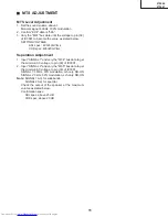
MTS ADJUSTMENT
MTS Level Adjustment
1. Set the sound volume above 1.
Monoral signal: 400Hz, 100% modulation
2. Confirm "EX4" data is "5Ah".
3. Vary the "M01" bus data until the voltage to pin (39)
of IC3001 to become the value as stated below.
SETTING VOLTAGE
ADJ spec : 490
±
10mVrms
CHK spec: 490
±
20mVrms
Separation Adjustment
1. Input "SIGNAL 1" and vary the "M04" bus data to get
the minimun AC voltage to pin (39) of IC3001.
2. Input "SIGNAL 2" and vary the "M05" bus data to get
the minimun AC voltage to pin (39) of IC3001.
SIGNAL 1: 300Hz, 30% modulation, Lch only, NR-ON
SIGNAL 2: 3kHz, 30% modulation, Lch only, NR-ON
Note: SIGNAL 1 Adj. for widebando
SIGNAL 2 Adj. for spectral
Check the output of the speaker at the maximum
volume as stated below.
Confirmation spec:
ADJ spec: above 25 dB
CHK spec: above 20 dB
Summary of Contents for 27F640
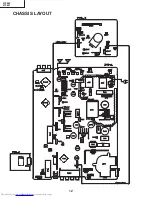
Page 12: ...12 27F640 27F641 CHASSIS LAYOUT ...
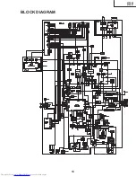
Page 13: ...13 27F640 27F641 BLOCK DIAGRAM ...
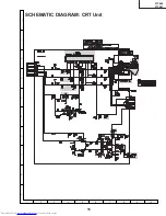
Page 15: ...15 27F640 27F641 1 2 3 4 5 6 7 8 9 10 A B C D E F G H I J SCHEMATIC DIAGRAM CRT Unit ...
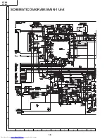
Page 16: ...16 27F640 27F641 1 2 3 4 5 6 7 8 9 10 A B C D E F G H I J SCHEMATIC DIAGRAM MAIN 1 Unit ...
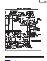
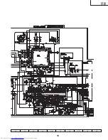
Page 17: ...17 27F640 27F641 10 11 12 13 14 15 16 17 18 19 ...
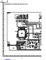
Page 18: ...18 27F640 27F641 1 2 3 4 5 6 7 8 9 10 A B C D E F G H I J SCHEMATIC DIAGRAM MAIN 2 Unit ...
Page 19: ...19 27F640 27F641 10 11 12 13 14 15 16 17 18 19 ...
Page 20: ...20 27F640 27F641 1 2 3 4 5 6 7 8 9 10 A B C D E F G H I J SCHEMATIC DIAGRAM 3 LINE Y C Unit ...
Page 21: ...21 27F640 27F641 10 11 12 13 14 15 16 17 18 19 ...
Page 23: ...23 27F640 27F641 10 11 12 13 14 15 16 17 18 19 ...
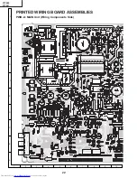
Page 24: ...24 27F640 27F641 1 2 3 4 5 6 7 8 9 10 A B C D E F G H I J PWB A MAIN Unit Components side ...
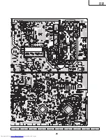
Page 25: ...25 27F640 27F641 10 11 12 13 14 15 16 17 18 19 ...


