14
14
Pinout and I/O Description
14
3.4
USB Device Interface
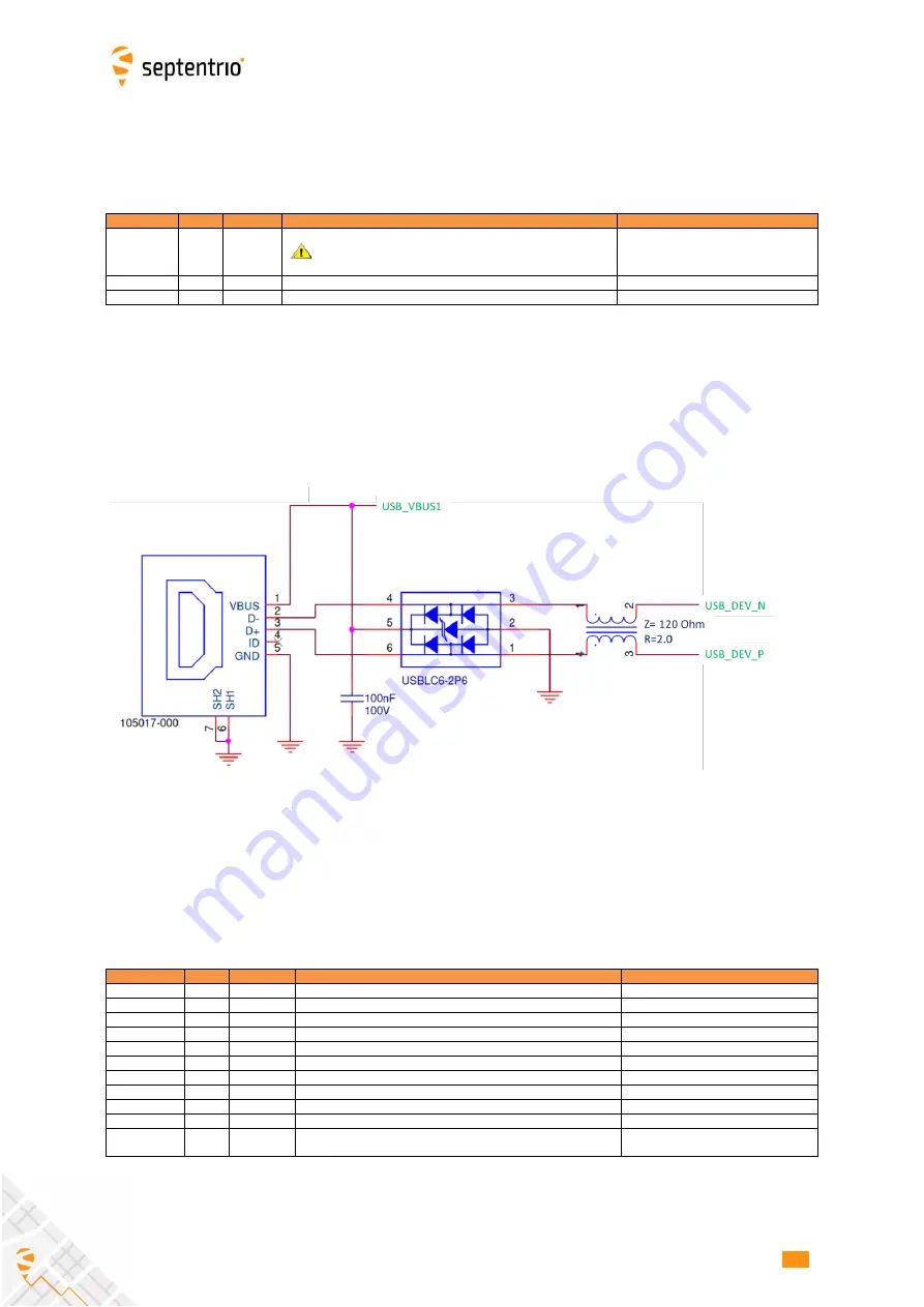
The following pins are used for accessing the module over USB in USB-device mode.
Pin Name
Type
Level
Description
Comment
USB_VBUS1
P,I
4.40V to
5.5V
USB VBUS input.
This pin cannot be used to power the module.
Maximal current drawn by the module is 50 mA.
USB_DEV_N
I/O
USB
USB data signal, negative
USB_DEV_P
I/O
USB
USB data signal, positive
USB is configured in USB 2.0 mode (high speed, 480Mbps max).
An example of an USB application circuit with ESD protection is shown below. The user
shall make sure to use an ESD-protection and common mode choke compatible with high-
speed USB if this is desired, for instance the USBLC6-2 from ST and DLP31SN121ML2L
from Murata.
3.5
Ethernet
The module supports full duplex 10/100 Base-T Ethernet communication. The Ethernet
PHY and magnetics are to be implemented on the host board. Connection with the PHY
is through the RMII interface available on the following pins:
Pin Name
Type
Level
Description
Comment
RMII_CLK
O
3V3_LVTTL
LAN PHY Clock
MDIO
I/O
3V3_LVTTL
LAN PHY control data
MDC
O
3V3_LVTTL
LAN PHY control clock
RMII_RXD1
I, PU
3V3_LVTTL
LAN PHY receive data 1
RMII_RXD0
I, PU
3V3_LVTTL
LAN PHY receive data 0
RMII_CRSDV
I, PU
3V3_LVTTL
LAN PHY CRS
RMII_RXER
I, PU
3V3_LVTTL
LAN PHY RX error
RMII_TXEN
O
3V3_LVTTL
LAN PHY transmit enable
RMII_TXD0
O
3V3_LVTTL
LAN PHY transmit data 0
RMII_TXD1
O
3V3_LVTTL
LAN PHY transmit data 1
nRST_LAN
O
3V3_LVTTL
LAN reset (low to reset the PHY)
When connecting this pin to enable an
Ethernet PHY, add a 10k pull-down.
If Ethernet is not used, all these pins should be left unconnected.


